 | ÐлекÑÑоннÑй компоненÑ: MC33253 | СкаÑаÑÑ:  PDF PDF  ZIP ZIP |
Äîêóìåíòàöèÿ è îïèñàíèÿ www.docs.chipfind.ru
MC33253
This document contains information on a new product. Specifications and information herein are
subject to change without notice.
Advance Information
Full Bridge Pre-Driver
Page 1/15
Order Number: MC33253/D
Rev 3, 03/2001
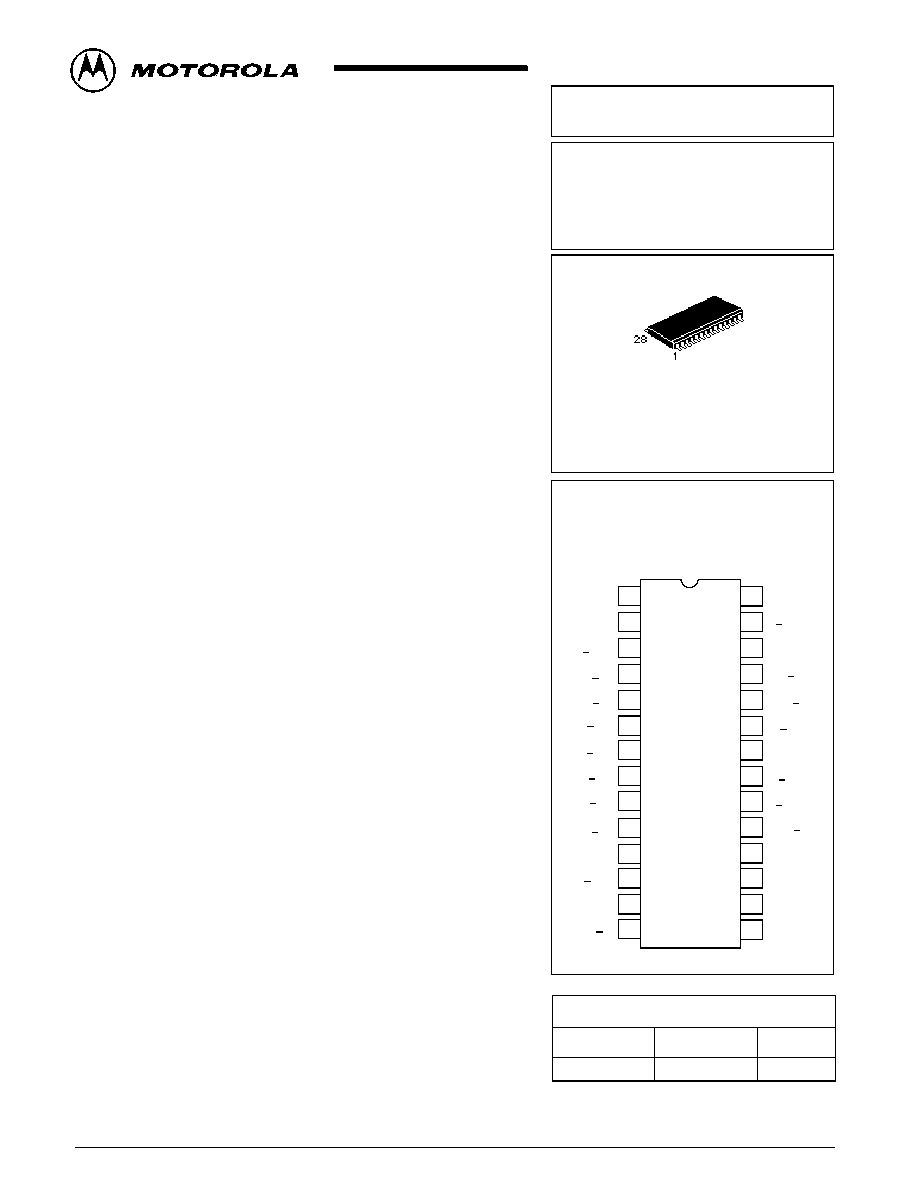
DW SUFFIX
(TOP VIEW)
CASE 751F-05
1
2
3
4
5
6
7
8
22
23
24
25
26
27
28
9
21
20
10
11
12
13
14
17
18
19
16
15
V
CC
C2
CP_OUT
SRC_HS
1
GATE_HS
1
/IN_HS
1
IN_HS
1
/IN_LS
1
IN_LS
1
GATE_LS
1
GND1
LR_OUT
V
CC2
GND_A
IS
OUT
G_EN
/CCS
GATE_HS
2
/IN_HS
2
IN_HS
2
IN_LS
2
GATE_LS
2
GND2
IS
+IN
C1
IS
-IN
SRC_HS
2
/IN_LS
2
PIN CONNECTIONS
PLASTIC PACKAGE
CASE 751F-05
PC33253DW
ORDERING INFORMATION
Device
Temperature
Range
Package
SOIC28
-40
o
C to +125
o
C
55 VOLTS
SEMICONDUCTOR
TECHNICAL DATA
© Motorola, Inc., 2001. All rights reserved.
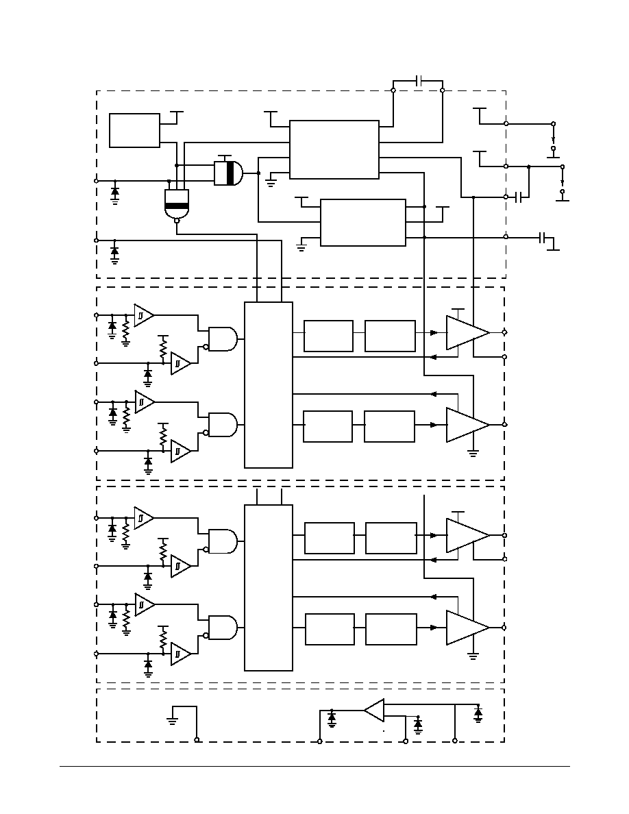
The MC33253 is a full bridge driver including integrated charge
pump, two independent high and low side driver channels.
The high and low side drivers include a cross conduction suppression
circuit, which, if enabled, prevents the external power FETs from being on
at the same time.
The drive outputs are capable to source and sink 1 A pulse peak
current. The low side channel is referenced to ground, the high side
channel is floating above ground.
A linear regulator provides a maximum of 15.5V to supply the low
side gate driver stages. The high side driver stages are supplied with a
10V charge pump voltage. Such built-in feature, associated to external
capacitor provides a full floating high side drive.
An under- and over-voltage protection prevents erratic system
operation at abnormal supply voltages. Under fault, these functions force
the driver stages into off state.
The logic inputs are compatible with standard CMOS or LSTTL
outputs. The input hysteresis makes the output switching time
independent of the input transition time.
The global enable logic signal can be used to disable the charge
pump and all the bias circuit. The net advantage is the reduction of the
quiescent supply current to under 10
µ
A. To wake up the circuit, 5 V has to
be provided at G_EN. A built-in single supply operational amplifier could
be used to feedback information from the output load to the external
MCU.
· V
CC
Operating Voltage Range from 5.5 V up to 55 V
· V
CC2
Operating Voltage Range from 5.5 V up to 28 V
· Automotive Temperature Range -40
°
C to 125
°
C
· 1A Pulse Current Output Driver
· Fast PWM Capability
· Built-In Charge Pump
· Cross Conduction Suppression Circuit
F
r
e
e
s
c
a
l
e
S
e
m
i
c
o
n
d
u
c
t
o
r
,
I
Freescale Semiconductor, Inc.
For More Information On This Product,
Go to: www.freescale.com
n
c
.
.
.
MC33253
MOTOROLA
rev3.0 - 2/15
MC33253
Figure 1. Principal Building Blocks
UV/OV
Detect
G_EN
/CCS
IN_HS1
/IN_HS1
IN_LS1
/IN_LS1
IN_HS2
/IN_HS2
IN_LS2
/IN_LS2
BRG_EN
CCS
GATE_LS1
SRC_HS1
GATE_HS1
CP_OUT
LR_OUT
GATE_LS2
SRC_HS2
GATE_HS2
5.5 V...
55 V
5.5 V...
28 V
Pulse
Generator
V
DD
/V
CC
Level Shift
Output
Driver
Pulse
Generator
V
DD
/V
POS
Level Shift
Output
Driver
G_LOW_LS
G_LOW_H
IN
IN
OUT
OUT
Input
&
CCS
LOGIC
V
CC
Linear
Reg
V
CC2
EN
GND
+13.5 V
+5.0 V
+13.5 V
V
DD
HIGH AND LOW SIDE CHANNEL
WITH CROSS CONDUCTION SUPPRESSION
HIGH AND LOW SIDE
Charge
Pump
RDY
EN
GND
C2
Vpos
+13.5 V
V
CC
C1
V
CC2
V
CC
V
CC
V
CC2
V
CC
V
CC2
Vgs_hs
Vgs_ls
Vgs_ls
V
CC
V
DD
C2
C1
V
DD
V
DD
CCS
BRG_EN
Pulse
Generator
V
DD
/V
CC
Level Shift
Output
Driver
Pulse
Generator
V
DD
/V
POS
Level Shift
Output
Driver
G_LOW_LS
G_LOW_H
IN
IN
OUT
OUT
Input
&
CCS
V
CC
HIGH AND LOW SIDE CHANNEL WITH
CROSS CONDUCTION SUPPRESSION
Vgs_ls
V
DD
V
DD
CCS
BRG_EN
SENSE CURRENT AMPLIFIER
-
+
GND
IS
OUT
IS
+IN
IS
-IN
CONTROL WITH CHARGE PUMP
CAO
CA
-
C
CP_OUT
C
LR_OUT
CA
+
Ccp
F
r
e
e
s
c
a
l
e
S
e
m
i
c
o
n
d
u
c
t
o
r
,
I
Freescale Semiconductor, Inc.
For More Information On This Product,
Go to: www.freescale.com
n
c
.
.
.
MC33253
MOTOROLA
rev3.0 - 3/15
MC33253
ABSOLUTE MAXIMUM RATINGS
Absolute Maximum Ratings indicate sustained limits beyond which damage to the device may occur. All voltage
parameters are absolute voltages referenced to GND.
NOTE1: VCC can sustain load dump pulse 40V, 400ms, 2Ohms
Rating
Symbol
Min
Max
Unit
Supply Voltage1
V
CC
-0.3
65
V
Supply Voltage2 (NOTE 1)
V
CC2
-0.3
35
V
Linear Regulator Output Voltage
V
LR_out
-0.3
18
V
High Side Floating Supply Absolute Voltage
V
CP_OUT
-0.3
65
V
High Side Floating Source Voltage
V
SRC_HS
-0.3
65
V
High Side Gate Voltage
V
GATE_HS
-0.3
65
V
High Side Gate Source Voltage
V
GATE_HS
- V
SRC_HS
-0.3
20
V
High Side Source Current from Cpout in Switch On State
I
S
250
mA
High Side Floating Supply Gate Voltage
V
CP_OUT
- V
GATE_HS
-0.3
65
V
Low Side Output Voltage
V
GATE_LS
-0.3
17
V
Wake up Voltage
V
G_EN
-0.3
35
V
Logic Input Voltage
V
IN
-0.3
10
V
Charge Pump Capacitor Voltage
V
C1
-0.3
V
LR_OUT
V
Charge Pump Capacitor Voltage
V
C2
-0.3
65
V
Operational Amplifier Output Voltage
V
CAO
-0.3
7
V
Operational Amplifier Inverting Input Voltage
V
CA
-
-0.3
7
V
Operational Amplifier Non Inverting Input Voltage
V
CA
+
-0.3
7
V
ESD Voltage on any Pins (HBM, 100pF, 1.5kOhms)
V
ESD
-2.0
2.0
kV
Power Dissipation and Thermal Characteristics
Maximum Power Dissipation@25°C
P
D
2
W
Thermal Resistance Junction-to-Air
R
JA
60
°
C/W
Operating Junction Temperature
T
J
-40
+150
°
C
Storage Temperature
T
stg
-65
+150
°
C
OPERATING CONDITIONS
Typical values for T
A
= 25
°
C, Min/Max values for T
A
= -40
°
C to +125
°
C
Rating
Symbol
Min
Max
Unit
Supply Voltage1
V
CC
5.5
55
V
Supply Voltage2
V
CC2
5.5
28
V
High Side Floating Supply Absolute Voltage
V
CP_OUT
V
CC
+4
V
CC
+11but<65
V
F
r
e
e
s
c
a
l
e
S
e
m
i
c
o
n
d
u
c
t
o
r
,
I
Freescale Semiconductor, Inc.
For More Information On This Product,
Go to: www.freescale.com
n
c
.
.
.
MC33253
MOTOROLA
rev3.0 - 4/15
MC33253
STATIC ELECTRICAL CHARACTERISTICS
V
CC
= 12 V, V
CC2
= 12 V, C
CP
= 33 nF, G_EN = 4.5 V unless otherwise specified.
Typical values for TA = 25
°
C, Min/Max values for TA = -40
°
C to +125
°
C, unless otherwise specified.
Characteristics
Pin #
Symbol
Min
Typ
Max
Unit
LOGIC SECTION
Logic "1" Input Voltage (IN_LS & IN_HS)
7, 9, 20, 22
V
IH
2.0
10
V
Logic "0" Input Voltage (IN_LS & IN_HS)
V
IL
0.8
V
Logic "1" Input Current Vin=5V
7, 9, 20, 22
I
in+
200
1000
uA
Logic "0" Input Current Vin=0V
I
in-
200
1000
uA
Logic "0" Input Voltage (/IN_LS & /IN_HS&/CCS)
6, 8, 21, 23,
26
V
IH
2.0
10
V
Logic "1" Input Voltage (/IN_LS & /IN_HS&/CCS)
V
IL
0.8
V
Logic "0" Input Current Vin=5V
6, 8, 21, 23,
26
I
in+
TBD
TBD
uA
Logic "1" Input Current Vin=0V
I
in-
TBD
TBD
uA
Wake Up Input Voltage (G_EN)
27
V
G_EN
4.5
5.0
V
CC2
V
Wake Up Current (G_EN) VG_EN = 14 V
27
I
G_EN
200
500
uA
LINEAR REGULATOR SECTION
Linear Regulator
V
LR_OUT
@ V
CC2
from 16.5 to 28 V, I
LOAD
from
0mA to 20mA
12
V
LR_OUT
13.5
16.5
V
Linear Regulator
V
LR_OUT
@ V
CC2
=
12 V, I
LOAD
= 20mA
12
V
LR_OUT
V
CC2
-
1.5
V
V
LR_OUT
@ V
CC2
=5.5
V, I
LOAD
=TBD, V
CC
= 5.5
V
12
TBD
V
CHARGE PUMP SECTION
Charge Pump Output Voltage, referenced to V
CC
I
LOAD
= 0mA, C
Cpout
=1uF
3
V
CP_OUT
V
LR_OUT
- 2
V
Charge Pump Output Voltage, referenced to V
CC
I
LOAD
= 7mA, C
Cpout
=1uF
3
V
CP_OUT
V
LR_OUT
-3
V
Charge Pump Output Voltage, referenced to V
CC
V
CC2
=
V
CC
=5.5V
I
LOAD
= 0mA, C
Cpout
=1uF
3
V
CP_OUT
V
LR_OUT
- TBD
V
Charge Pump Output Voltage, referenced to V
CC
V
CC2
=
V
CC
=5.5V
I
LOAD
= 7mA, C
Cpout
=1uF
3
V
CP_OUT
V
LR_OUT-
-TBD
V
Peak current through pin 15under rapid changing
Vcc voltages (see Figure 6)
15
I
C1
-2.0
2.0
A
Minimum peak voltage at pin 15under rapid
changing Vcc voltages (see Figure 6)
15
V
C1
min
-1.5
V
SUPPLY VOLTAGE SECTION
Quiescent Vcc Supply Current V
G_EN
=0V
1
TBD
uA
Operating Vcc Supply Current
(@V
CC
=55V and V
CC2
=28V)
(@V
CC
=12V and V
CC2
=12V)
1
1
TBD
TBD
mA
mA
Quiescent Vcc2 Supply Current V
G_EN
=0V
13
TBD
uA
F
r
e
e
s
c
a
l
e
S
e
m
i
c
o
n
d
u
c
t
o
r
,
I
Freescale Semiconductor, Inc.
For More Information On This Product,
Go to: www.freescale.com
n
c
.
.
.
MC33253
MOTOROLA
rev3.0 - 5/15
MC33253
Operating Vcc2 Supply Current
(@V
CC
=55V and V
CC2
=28V)
(@V
CC
=12V and V
CC2
=12V)
Logic pin inactive (high impedance)
13
13
10
8
mA
Under Voltage Shutdown V
CC2
(Note2)
13
UV2
4.6
5.1
5.5
V
Under Voltage Shutdown V
CC
1
UV
4.6
5.1
5.5
V
Over Voltage Shutdown V
CC
1
OV
57
61
64
V
Over Voltage Shutdown V
CC2
13
OV2
29.5
31
32.5
V
OUTPUT SECTION
Output Sink Resistance (Turned off)
V
GATE_HS
- V
SRC_HS
=1V
3, 4, 5, 10,
19, 24, 25
R
DS
22.0
Ohms
Output Source Resistance (Turned on)
V
CP_OUT
- V
GATE_HS
=0.1V
R
DS
22.0
Ohms
High Side Source Current from Cpout in Switch
On State
4, 25
I
S
max
200
mA
Max Voltage (V
GATE_HS
- V
SRC_HS)
,
INH=1, I
Smax
=200mA
4, 5, 24, 25
18
V
SENSE CURRENT AMPLIFIER SECTION
(Internal VCC supply @ 12V)
Output Dynamic Range (I
sink/source
= 200
µ
A)
28
V
OH
V
OL
4.7
5.0
300
V
mV
Open Loop Gain (at 25
°
C) A
50
dB
Input Bias Current
16, 17
I
IB
1.0
uA
Input Offset Voltage (at 25
°
C)
V
io
-5.0
2.0
5.0
mV
Input Common Mode Voltage Range
ICMR
0
5
V
Common Mode Rejection Ratio
CMRR
70
dB
Sink Capability (Vo>1.1V) (Note 3)
28
I
sink
2.0
3.0
mA
Source Capability (Vo<5V) (Note 3)
28
I
source
2.0
3.0
mA
Gain Bandwidth Product
GBW
1.8
MHz
Operational Amplifier Output Voltage, I
sink=500uA
28
V
CAO
0.5
V
Operational Amplifier Output Voltage,
I
source=500uA
28
V
CAO
5
V
Operational Amplifier Slew Rate (+)
SR+
1
V/us
Operational Amplifier Slew Rate (-)
SR-
1
V/us
Characteristics
Pin #
Symbol
Min
Typ
Max
Unit
F
r
e
e
s
c
a
l
e
S
e
m
i
c
o
n
d
u
c
t
o
r
,
I
Freescale Semiconductor, Inc.
For More Information On This Product,
Go to: www.freescale.com
n
c
.
.
.
Document Outline
- Figure�1.� Principal Building Blocks
- ABSOLUTE MAXIMUM RATINGS Absolute Maximum Ratings indicate sustained limits beyond which damage t...
- Rating
- Symbol
- Min
- Max
- Unit
- Rating
- Symbol
- Min
- Max
- Unit
- Characteristics
- Pin #
- Symbol
- Min
- Typ
- Max
- Unit
- Logic 1 Input Voltage (IN_LS & IN_HS)
- 7, 9, 20, 22
- VIH
- 2.0
- 10
- V
- Logic 0 Input Voltage (IN_LS & IN_HS)
- VIL
- 0.8
- V
- Logic 1 Input Current Vin=5V
- 7, 9, 20, 22
- Iin+
- 200
- 1000
- uA
- Logic 0 Input Current Vin=0V
- Iin-
- 200
- 1000
- uA
- Logic 0 Input Voltage (/IN_LS & /IN_HS&/CCS)
- 6, 8, 21, 23, 26
- VIH
- 2.0
- 10
- V
- Logic 1 Input Voltage (/IN_LS & /IN_HS&/CCS)
- VIL
- 0.8
- V
- Logic 0 Input Current Vin=5V
- 6, 8, 21, 23, 26
- Iin+
- TBD
- TBD
- uA
- Logic 1 Input Current Vin=0V
- Iin-
- TBD
- TBD
- uA
- Wake Up Input Voltage (G_EN)
- 27
- VG_EN
- 4.5
- 5.0
- VCC2
- V
- Wake Up Current (G_EN) VG_EN = 14 V
- 27
- IG_EN
- 200
- 500
- uA
- Linear Regulator
- VLR_OUT @ VCC2 from 16.5 to 28 V, ILOAD from 0mA to 20mA
- 12
- VLR_OUT
- 13.5
- 16.5
- V
- Linear Regulator
- VLR_OUT @ VCC2 =12 V, ILOAD = 20mA
- 12
- VLR_OUT
- VCC2 - 1.5
- V
- 12
- TBD
- V
- Charge Pump Output Voltage, referenced to VCC
- ILOAD = 0mA, CCpout=1uF
- 3
- VCP_OUT
- VLR_OUT
- - 2
- V
- Charge Pump Output Voltage, referenced to VCC
- ILOAD = 7mA, CCpout=1uF
- 3
- VCP_OUT
- VLR_OUT
- -3
- V
- Charge Pump Output Voltage, referenced to VCC VCC2 = VCC=5.5V
- ILOAD = 0mA, CCpout=1uF
- 3
- VCP_OUT
- VLR_OUT
- - TBD
- V
- Charge Pump Output Voltage, referenced to VCC
- VCC2 = VCC=5.5V
- ILOAD = 7mA, CCpout=1uF
- 3
- VCP_OUT
- VLR_OUT-
- -TBD
- V
- Peak current through pin 15under rapid changing Vcc voltages (see Figure�6)
- 15
- IC1
- -2.0
- 2.0
- A
- Minimum peak voltage at pin 15under rapid changing Vcc voltages (see Figure�6)
- 15
- VC1min
- -1.5
- V
- Quiescent Vcc Supply Current VG_EN=0V
- 1
- TBD
- uA
- Operating Vcc Supply Current
- (@VCC=55V and VCC2=28V)
- (@VCC=12V and VCC2=12V)
- 1
- 1
- TBD
- TBD
- mA
- mA
- Quiescent Vcc2 Supply Current VG_EN=0V
- 13
- TBD
- uA
- Operating Vcc2 Supply Current
- (@VCC=55V and VCC2=28V)
- (@VCC=12V and VCC2=12V)
- Logic pin inactive (high impedance)
- 13
- 13
- 10
- 8
- mA
- Under Voltage Shutdown VCC2 (Note2)
- 13
- UV2
- 4.6
- 5.1
- 5.5
- V
- Under Voltage Shutdown VCC
- 1
- UV
- 4.6
- 5.1
- 5.5
- V
- Over Voltage Shutdown VCC
- 1
- OV
- 57
- 61
- 64
- V
- Over Voltage Shutdown VCC2
- 13
- OV2
- 29.5
- 31
- 32.5
- V
- Output Sink Resistance (Turned off)
- VGATE_HS - VSRC_HS =1V
- 3, 4, 5, 10, 19, 24, 25
- RDS
- 22.0
- Ohms
- Output Source Resistance (Turned on)
- VCP_OUT - VGATE_HS =0.1V
- RDS
- 22.0
- Ohms
- High Side Source Current from Cpout in Switch On State
- ISmax
- 200
- mA
- 4, 5, 24, 25
- 18
- V
- Output Dynamic Range (Isink/source = 200mA)
- 28
- VOH
- VOL
- 4.7
- 5.0
- 300
- V
- mV
- Open Loop Gain (at 25°C)
- A
- 50
- dB
- Input Bias Current
- 16, 17
- IIB
- 1.0
- uA
- Input Offset Voltage (at 25°C)
- Vio
- -5.0
- 2.0
- 5.0
- mV
- Input Common Mode Voltage Range
- ICMR
- 0
- 5
- V
- Common Mode Rejection Ratio
- CMRR
- 70
- dB
- Sink Capability (Vo>1.1V) (Note 3)
- 28
- Isink
- 2.0
- 3.0
- mA
- Source Capability (Vo<5V) (Note 3)
- 28
- Isource
- 2.0
- 3.0
- mA
- Gain Bandwidth Product
- GBW
- 1.8
- MHz
- Operational Amplifier Output Voltage, Isink=500uA
- 28
- VCAO
- 0.5
- V
- Operational Amplifier Output Voltage, Isource=500uA
- 28
- VCAO
- 5
- V
- Operational Amplifier Slew Rate (+)
- SR+
- 1
- V/us
- Operational Amplifier Slew Rate (-)
- SR-
- 1
- V/us
- DYNAMIC ELECTRICAL CHARACTERISTICS VCC = 12 V, VCC2 = 12 V, CCP = 33 nF, G_EN = 4.5 V unless othe...
- Typical values for TA = 25°C, Min/Max values for TA = -40°C to +125°C, unless otherwise specified.
- Characteristics
- Pin #
- Symbol
- Min
- Typ
- Max
- Unit
- Prop. Delay HS and LS, Cload=5nF;
- Between 50% Input to 50% Output
- (see Figure�2)
- 5, 6, 7, 8, 9, 20, 21, 22, 23
- tPD
- 200
- 300
- ns
- Turn On Rise Time, Cload=5nF ;
- 10% to 90% (NOTE 4) (see Figure�2)
- 5, 10, 19, 24
- tr
- 80
- 180
- ns
- Turn Off Fall Time, Cload=5nF ;
- 10% to 90% (NOTE 4) (see Figure�2)
- tf
- 80
- 180
- ns
- NOTE 2: Between 4.6V and 5.5V, the device has been a non erroneous behaviour.
- NOTE 3: Input overdrive 1V
- NOTE 4: Rise time is given by time needed to charge the gate from 1V to 10V (Vice versa for fall ...
- NOTE : Cload corresponds to a capacitor between GATE_HS and SRC_HS for the high side and between ...
- Driver Characteristics
- Driver Supply
- TMOS Failure Protection
- Logic Inputs
- Low Drop Linear Regulator
- Charge Pump
- Ccp
- OP-Amp
- Pin
- Symbol
- Pin Description