 | –≠–ª–µ–∫—Ç—Ä–æ–Ω–Ω—ã–π –∫–æ–º–ø–æ–Ω–µ–Ω—Ç: MC33341D | –°–∫–∞—á–∞—Ç—å:  PDF PDF  ZIP ZIP |
Device
Operating
Temperature Range
Package
MC33341
SEMICONDUCTOR
TECHNICAL DATA
POWER SUPPLY
BATTERY CHARGER
REGULATION
CONTROL CIRCUIT
ORDERING INFORMATION
MC33341D
MC33341P
TA = ≠25
∞
to +85
∞
C
SO≠8
Plastic DIP
P SUFFIX
PLASTIC PACKAGE
CASE 626
8
1
1
8
7
6
5
2
3
4
(Top View)
Current Sense
Input A
Current Threshold
Adjust
Compensation
Drive Output
PIN CONNECTIONS
Order this document by MC33341/D
8
1
D SUFFIX
PLASTIC PACKAGE
CASE 751
(SO≠8)
Gnd
VCC
Current Sense Input B/
Voltage Threshold Adjust
Voltage Sense Input
1
MOTOROLA ANALOG IC DEVICE DATA
Advance Information
Power Supply
Battery Charger
Regulation Control Circuit
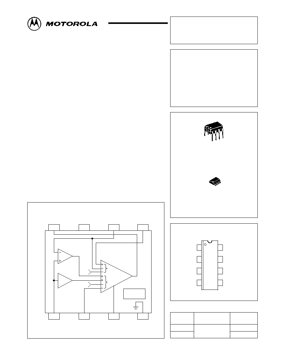
The MC33341 is a monolithic regulation control circuit that is specifically
designed to close the voltage and current feedback loops in power supply
and battery charger applications. This device features the unique ability to
perform source high≠side, load high≠side, source low≠side and load
low≠side current sensing, each with either an internally fixed or externally
adjustable threshold. The various current sensing modes are accomplished
by a means of selectively using the internal differential amplifier, inverting
amplifier, or a direct input path. Positive voltage sensing is performed by an
internal voltage amplifier. The voltage amplifier threshold is internally fixed
and can be externally adjusted in all low≠side current sensing applications.
An active high drive output is provided to directly interface with economical
optoisolators for isolated output power systems. This device is available in
8≠lead dual≠in≠line and surface mount packages.
∑
Differential Amplifier for High≠Side Source and Load Current Sensing
∑
Inverting Amplifier for Source Return Low≠Side Current Sensing
∑
Non≠Inverting Input Path for Load Low≠Side Current Sensing
∑
Fixed or Adjustable Current Threshold in All Current Sensing Modes
∑
Positive Voltage Sensing in All Current Sensing Modes
∑
Fixed Voltage Threshold in All Current Sensing Modes
∑
Adjustable Voltage Threshold in All Low≠Side Current Sensing Modes
∑
Output Driver Directly Interfaces with Economical Optoisolators
∑
Operating Voltage Range of 2.3 V to 16 V
Representative Block Diagram
This device contains 114 active transistors.
8
Drive
Output
1
Current Sense
Input A
7
VCC
2
Current
Threshold Adjust
6
Current Sense Input B/
Voltage Threshold Adjust
3
Compensation
5
Voltage Sense
Input
4
Gnd
Differential
Amp
Inverting/
Noninverting Amp
V
I
0.2 V
1.2 V
Reference
Voltage and Current
Transconductance
Amp/Driver
1.0
#
1.0
This document contains information on a new product. Specifications and information herein
are subject to change without notice.
©
Motorola, Inc. 1996
Rev 0
MC33341
2
MOTOROLA ANALOG IC DEVICE DATA
MAXIMUM RATINGS
Rating
Symbol
Value
Unit
¡¡¡¡¡¡¡¡¡¡¡¡¡¡¡
¡¡¡¡¡¡¡¡¡¡¡¡¡¡¡
Power Supply Voltage (Pin 7)
¡¡¡¡
¡¡¡¡
VCC
¡¡¡¡
¡¡¡¡
16
¡¡¡
¡¡¡
V
¡¡¡¡¡¡¡¡¡¡¡¡¡¡¡
¡
¡¡¡¡¡¡¡¡¡¡¡¡¡¡
¡
¡¡¡¡¡¡¡¡¡¡¡¡¡¡
¡
¡¡¡¡¡¡¡¡¡¡¡¡¡¡
¡
¡¡¡¡¡¡¡¡¡¡¡¡¡¡
¡¡¡¡¡¡¡¡¡¡¡¡¡¡¡
Voltage Range
Current Sense Input A (Pin 1)
Current Threshold Adjust (Pin 2)
Compensation (Pin 3)
Voltage Sense Input (Pin 5)
Current Sense Input B/Voltage Threshold Adjust (Pin 6)
Drive Output (Pin 8)
¡¡¡¡
¡
¡¡
¡
¡
¡¡
¡
¡
¡¡
¡
¡
¡¡
¡
¡¡¡¡
VIR
¡¡¡¡
¡
¡¡¡
¡
¡¡¡
¡
¡¡¡
¡
¡¡¡
¡¡¡¡
≠1.0 to VCC
¡¡¡
¡
¡
¡
¡
¡
¡
¡
¡
¡
¡
¡
¡
¡¡¡
V
Drive Output Source Current (Pin 8)
ISource
50
mA
¡¡¡¡¡¡¡¡¡¡¡¡¡¡¡
¡
¡¡¡¡¡¡¡¡¡¡¡¡¡¡
¡¡¡¡¡¡¡¡¡¡¡¡¡¡¡
Thermal Resistance, Junction≠to≠Air
P Suffix, DIP Plastic Package, Case 626
D Suffix, SO≠8 Plastic Package, Case 751
¡¡¡¡
¡
¡¡
¡
¡¡¡¡
R
JA
¡¡¡¡
¡
¡¡¡
¡¡¡¡
100
178
¡¡¡
¡
¡
¡
¡¡¡
∞
C/W
¡¡¡¡¡¡¡¡¡¡¡¡¡¡¡
¡¡¡¡¡¡¡¡¡¡¡¡¡¡¡
Operating Junction Temperature (Note 1)
¡¡¡¡
¡¡¡¡
TJ
¡¡¡¡
¡¡¡¡
≠25 to +150
¡¡¡
¡¡¡
∞
C
¡¡¡¡¡¡¡¡¡¡¡¡¡¡¡
¡¡¡¡¡¡¡¡¡¡¡¡¡¡¡
Storage Temperature
¡¡¡¡
¡¡¡¡
Tstg
¡¡¡¡
¡¡¡¡
≠55 to +150
¡¡¡
¡¡¡
∞
C
NOTE: ESD data available upon request.
ELECTRICAL CHARACTERISTICS
(VCC = 6.0 V, TA = 25
∞
C, for min/max values TA is the operating junction
temperature range that applies (Note 1), unless otherwise noted.)
Characteristic
Symbol
Min
Typ
Max
Unit
¡¡¡¡¡¡¡¡¡¡¡¡¡¡¡¡¡¡¡¡¡¡¡¡¡¡¡¡¡¡¡¡¡¡
¡¡¡¡¡¡¡¡¡¡¡¡¡¡¡¡¡¡¡¡¡¡¡¡¡¡¡¡¡¡¡¡¡¡
CURRENT SENSING (Pins 1, 2, 6)
¡¡¡¡¡¡¡¡¡¡¡¡¡¡¡¡¡¡
¡¡¡¡¡¡¡¡¡¡¡¡¡¡¡¡¡¡
High≠Side Source and Load Sensing Pin 1 to Pin 6 (Pin 1 >1.6 V)
¡¡¡¡
¡¡¡¡
Vth(I HS)
¡¡¡¡¡
¡¡¡¡¡
¡¡¡¡¡
¡¡¡¡¡
¡¡¡¡
¡¡¡¡
¡¡¡
¡¡¡
mV
Internally Fixed Threshold Voltage (Pin 2 = VCC)
TA = 25
∞
C
187
197
207
TA = Tlow to Thigh
183
≠
211
Externally Adjusted Threshold Voltage (Pin 2 = 0 V)
≠
10
≠
Externally Adjusted Threshold Voltage (Pin 2 = 200 mV)
≠
180
≠
¡¡¡¡¡¡¡¡¡¡¡¡¡¡¡¡¡¡
¡¡¡¡¡¡¡¡¡¡¡¡¡¡¡¡¡¡
Low≠Side Load Sensing Pin 1 to Pin 4 (Pin 1 = 0 V to 0.8 V)
¡¡¡¡
¡¡¡¡
Vth(I LS+)
¡¡¡¡¡
¡¡¡¡¡
¡¡¡¡¡
¡¡¡¡¡
¡¡¡¡
¡¡¡¡
¡¡¡
¡¡¡
mV
Internally Fixed Threshold Voltage (Pin 2 = VCC)
TA = 25
∞
C
194
200
206
TA = Tlow to Thigh
192
≠
208
Externally Adjusted Threshold Voltage (Pin 2 = 0 V)
≠
10
≠
Externally Adjusted Threshold Voltage (Pin 2 = 200 mV)
≠
180
≠
¡¡¡¡¡¡¡¡¡¡¡¡¡¡¡¡¡¡
¡¡¡¡¡¡¡¡¡¡¡¡¡¡¡¡¡¡
Low≠Side Source Return Sensing Pin 1 to 4 (Pin 1 = 0 V to ≠0.2 V)
¡¡¡¡
¡¡¡¡
Vth(I LS≠)
¡¡¡¡¡
¡¡¡¡¡
¡¡¡¡¡
¡¡¡¡¡
¡¡¡¡
¡¡¡¡
¡¡¡
¡¡¡
mV
Internally Fixed Threshold Voltage (Pin 2 = VCC)
TA = 25
∞
C
≠195
≠201
≠207
TA = Tlow to Thigh
≠193
≠
≠209
Externally Adjusted Threshold Voltage (Pin 2 = 0 V)
≠
≠10
≠
Externally Adjusted Threshold Voltage (Pin 2 = 200 mV)
≠
≠180
≠
¡¡¡¡¡¡¡¡¡¡¡¡¡¡¡¡¡¡
¡¡¡¡¡¡¡¡¡¡¡¡¡¡¡¡¡¡
Current Sense Input A (Pin 1)
¡¡¡¡
¡¡¡¡
¡¡¡¡¡
¡¡¡¡¡
¡¡¡¡¡
¡¡¡¡¡
¡¡¡¡
¡¡¡¡
¡¡¡
¡¡¡
Input Bias Current, High≠Side Source and Load Sensing
(Pin 2 = 0 V to VPin 6 V)
IIB(A HS)
≠
40
≠
µ
A
Input Bias Current, Low≠Side Load Sensing
(Pin 2 = 0 V to 0.8 V)
IIB(A LS+)
≠
10
≠
nA
Input Resistance, Low≠Side Source Return Sensing
(Pin 2 = ≠0.6 V to 0 V)
Rin(A LS≠)
≠
10
≠
k
¡¡¡¡¡¡¡¡¡¡¡¡¡¡¡¡¡¡
¡¡¡¡¡¡¡¡¡¡¡¡¡¡¡¡¡¡
Current Sense Input B/Voltage Threshold Adjust (Pin 6)
¡¡¡¡
¡¡¡¡
IIB(B)
¡¡¡¡¡
¡¡¡¡¡
¡¡¡¡¡
¡¡¡¡¡
¡¡¡¡
¡¡¡¡
¡¡¡
¡¡¡
Input Bias Current
High≠Side Source and Load Current Sensing (Pin 6 > 2.0 V)
≠
20
≠
µ
A
Voltage Threshold Adjust (Pin 6 < 1.2 V)
≠
100
≠
nA
¡¡¡¡¡¡¡¡¡¡¡¡¡¡¡¡¡¡
¡¡¡¡¡¡¡¡¡¡¡¡¡¡¡¡¡¡
Current Sense Threshold Adjust (Pin 2)
¡¡¡¡
¡¡¡¡
IIB(I th)
¡¡¡¡¡
¡¡¡¡¡
≠
¡¡¡¡¡
¡¡¡¡¡
10
¡¡¡¡
¡¡¡¡
≠
¡¡¡
¡¡¡
nA
Input Bias Current
¡¡¡¡¡¡¡¡¡¡¡¡¡¡¡¡¡¡
¡¡¡¡¡¡¡¡¡¡¡¡¡¡¡¡¡¡
Transconductance, Current Sensing Inputs to Drive Output
¡¡¡¡
¡¡¡¡
gm(I)
¡¡¡¡¡
¡¡¡¡¡
≠
¡¡¡¡¡
¡¡¡¡¡
6.0
¡¡¡¡
¡¡¡¡
≠
¡¡¡
¡¡¡
mhos
NOTE: 1. Tested ambient temperature range for the MC33341: Tlow = ≠25
∞
C, Thigh = +85
∞
C.

MC33341
3
MOTOROLA ANALOG IC DEVICE DATA
ELECTRICAL CHARACTERISTICS
(continued) (VCC = 6.0 V, TA = 25
∞
C, for min/max values TA is the operating junction
temperature range that applies (Note 1), unless otherwise noted.)
Characteristic
Unit
Max
Typ
Min
Symbol
¡¡¡¡¡¡¡¡¡¡¡¡¡¡¡¡¡¡¡¡¡¡¡¡¡¡¡¡¡¡¡¡¡¡
¡¡¡¡¡¡¡¡¡¡¡¡¡¡¡¡¡¡¡¡¡¡¡¡¡¡¡¡¡¡¡¡¡¡
DIFFERENTIAL AMPLIFIER DISABLE LOGIC (Pins 1, 6)
¡¡¡¡¡¡¡¡¡¡¡¡¡¡¡¡¡¡
¡¡¡¡¡¡¡¡¡¡¡¡¡¡¡¡¡¡
Logic Threshold Voltage Pin 1 (Pin 6 = 0 V)
¡¡¡¡
¡¡¡¡
¡¡¡¡¡
¡¡¡¡¡
¡¡¡¡¡
¡¡¡¡¡
¡¡¡¡
¡¡¡¡
¡¡¡
¡¡¡
V
Enabled, High≠Side Source and Load Current Sensing
Vth(I HS)
≠
1.7
≠
Disabled, Low≠Side Load and Source Return Current Sensing
Vth(I LS)
≠
1.3
≠
¡¡¡¡¡¡¡¡¡¡¡¡¡¡¡¡¡¡¡¡¡¡¡¡¡¡¡¡¡¡¡¡¡¡
¡¡¡¡¡¡¡¡¡¡¡¡¡¡¡¡¡¡¡¡¡¡¡¡¡¡¡¡¡¡¡¡¡¡
VOLTAGE SENSING (Pins 5, 6)
¡¡¡¡¡¡¡¡¡¡¡¡¡¡¡¡¡¡
¡¡¡¡¡¡¡¡¡¡¡¡¡¡¡¡¡¡
Positive Sensing Pin 5 to Pin 4
¡¡¡¡
¡¡¡¡
Vth(V)
¡¡¡¡¡
¡¡¡¡¡
¡¡¡¡¡
¡¡¡¡¡
¡¡¡¡
¡¡¡¡
¡¡¡
¡¡¡
Internally Fixed Threshold Voltage
TA = 25
∞
C
1.186
1.210
1.234
V
TA = Tlow to Thigh
1.174
≠
1.246
V
Externally Adjusted Threshold Voltage (Pin 6 = 0 V)
≠
40
≠
mV
Externally Adjusted Threshold Voltage (Pin 6 = 1.2 V)
≠
1.175
≠
V
¡¡¡¡¡¡¡¡¡¡¡¡¡¡¡¡¡¡
¡¡¡¡¡¡¡¡¡¡¡¡¡¡¡¡¡¡
Voltage Sense, Input Bias Current (Pin 5)
¡¡¡¡
¡¡¡¡
IIB(V)
¡¡¡¡¡
¡¡¡¡¡
≠
¡¡¡¡¡
¡¡¡¡¡
10
¡¡¡¡
¡¡¡¡
≠
¡¡¡
¡¡¡
nA
¡¡¡¡¡¡¡¡¡¡¡¡¡¡¡¡¡¡
¡¡¡¡¡¡¡¡¡¡¡¡¡¡¡¡¡¡
Transconductance, Voltage Sensing Inputs to Drive Output
¡¡¡¡
¡¡¡¡
gm(V)
¡¡¡¡¡
¡¡¡¡¡
≠
¡¡¡¡¡
¡¡¡¡¡
7.0
¡¡¡¡
¡¡¡¡
≠
¡¡¡
¡¡¡
mhos
¡¡¡¡¡¡¡¡¡¡¡¡¡¡¡¡¡¡¡¡¡¡¡¡¡¡¡¡¡¡¡¡¡¡
¡¡¡¡¡¡¡¡¡¡¡¡¡¡¡¡¡¡¡¡¡¡¡¡¡¡¡¡¡¡¡¡¡¡
DRIVE OUTPUT (Pin 8)
¡¡¡¡¡¡¡¡¡¡¡¡¡¡¡¡¡¡
¡¡¡¡¡¡¡¡¡¡¡¡¡¡¡¡¡¡
High State Source Voltage (ISource = 10 mA)
¡¡¡¡
¡¡¡¡
VOH
¡¡¡¡¡
¡¡¡¡¡
≠
¡¡¡¡¡
¡¡¡¡¡
VCC ≠ 0.8
¡¡¡¡
¡¡¡¡
≠
¡¡¡
¡¡¡
V
¡¡¡¡¡¡¡¡¡¡¡¡¡¡¡¡¡¡
¡¡¡¡¡¡¡¡¡¡¡¡¡¡¡¡¡¡
High State Source Current (Pin 8 = 0 V)
¡¡¡¡
¡¡¡¡
ISource
¡¡¡¡¡
¡¡¡¡¡
15
¡¡¡¡¡
¡¡¡¡¡
20
¡¡¡¡
¡¡¡¡
≠
¡¡¡
¡¡¡
mA
¡¡¡¡¡¡¡¡¡¡¡¡¡¡¡¡¡¡¡¡¡¡¡¡¡¡¡¡¡¡¡¡¡¡
¡¡¡¡¡¡¡¡¡¡¡¡¡¡¡¡¡¡¡¡¡¡¡¡¡¡¡¡¡¡¡¡¡¡
TOTAL DEVICE (Pin 7)
¡¡¡¡¡¡¡¡¡¡¡¡¡¡¡¡¡¡
¡¡¡¡¡¡¡¡¡¡¡¡¡¡¡¡¡¡
Operating Voltage Range
¡¡¡¡
¡¡¡¡
VCC
¡¡¡¡¡
¡¡¡¡¡
2.5 to 15
¡¡¡¡¡
¡¡¡¡¡
2.3 to 15
¡¡¡¡
¡¡¡¡
≠
¡¡¡
¡¡¡
V
¡¡¡¡¡¡¡¡¡¡¡¡¡¡¡¡¡¡
Power Supply Current (VCC = 6.0 V)
¡¡¡¡
ICC
¡¡¡¡¡
≠
¡¡¡¡¡
300
¡¡¡¡
600
¡¡¡
µ
A
NOTE: 1. Tested ambient temperature range for the MC33341: Tlow = ≠25
∞
C, Thigh = +85
∞
C.
PIN FUNCTION DESCRIPTION
Pin
Name
Description
¡¡¡
¡
¡
¡
¡
¡
¡
¡
¡
¡
¡
¡
¡
¡¡¡
1
¡¡¡¡¡¡¡¡
¡
¡¡¡¡¡¡
¡
¡
¡¡¡¡¡¡
¡
¡
¡¡¡¡¡¡
¡
¡
¡¡¡¡¡¡
¡
¡¡¡¡¡¡¡¡
Current Sense Input A
¡¡¡¡¡¡¡¡¡¡¡¡¡¡¡¡¡¡¡¡¡¡¡¡¡
¡
¡¡¡¡¡¡¡¡¡¡¡¡¡¡¡¡¡¡¡¡¡¡¡
¡
¡
¡¡¡¡¡¡¡¡¡¡¡¡¡¡¡¡¡¡¡¡¡¡¡
¡
¡
¡¡¡¡¡¡¡¡¡¡¡¡¡¡¡¡¡¡¡¡¡¡¡
¡
¡
¡¡¡¡¡¡¡¡¡¡¡¡¡¡¡¡¡¡¡¡¡¡¡
¡
¡¡¡¡¡¡¡¡¡¡¡¡¡¡¡¡¡¡¡¡¡¡¡¡¡
This multi≠mode current sensing input can be used for either source high≠side, load high≠side,
source≠return low≠side, or load low≠side sensing. It is common to a Differential Amplifier, Inverting
Amplifier, and a Noninverting input path. Each of these sensing paths indirectly connect to the current
sense input of the Transconductance Amplifier. This input is connected to the high potential side of a
current sense resistor when used in source high≠side, load high≠side, or load low≠side current
sensing modes. In source return low≠side current sensing mode, this pin connects to the low potential
side of a current sense resistor.
¡¡¡
¡
¡
¡
¡¡¡
2
¡¡¡¡¡¡¡¡
¡
¡¡¡¡¡¡
¡
¡¡¡¡¡¡¡¡
Current Threshold Adjust
¡¡¡¡¡¡¡¡¡¡¡¡¡¡¡¡¡¡¡¡¡¡¡¡¡
¡
¡¡¡¡¡¡¡¡¡¡¡¡¡¡¡¡¡¡¡¡¡¡¡
¡
¡¡¡¡¡¡¡¡¡¡¡¡¡¡¡¡¡¡¡¡¡¡¡¡¡
The current sense threshold can be externally adjusted over a range of 0 V to 200 mV with respect to
Pin 4, or internally fixed at 200 mV by connecting Pin 2 to VCC.
¡¡¡
¡
¡
¡
¡¡¡
3
¡¡¡¡¡¡¡¡
¡
¡¡¡¡¡¡
¡
¡¡¡¡¡¡¡¡
Compensation
¡¡¡¡¡¡¡¡¡¡¡¡¡¡¡¡¡¡¡¡¡¡¡¡¡
¡
¡¡¡¡¡¡¡¡¡¡¡¡¡¡¡¡¡¡¡¡¡¡¡
¡
¡¡¡¡¡¡¡¡¡¡¡¡¡¡¡¡¡¡¡¡¡¡¡¡¡
This pin is connected to a high impedance node within the transconductance amplifier and is made
available for loop compensation. It can also be used as an input to directly control the Drive Output.
An active low at this pin will force the Drive Output into a high state.
¡¡¡
¡¡¡
4
¡¡¡¡¡¡¡¡
¡¡¡¡¡¡¡¡
Ground
¡¡¡¡¡¡¡¡¡¡¡¡¡¡¡¡¡¡¡¡¡¡¡¡¡
¡¡¡¡¡¡¡¡¡¡¡¡¡¡¡¡¡¡¡¡¡¡¡¡¡
This pin is the regulation control IC ground. The control threshold voltages are with respect to this pin.
¡¡¡
¡
¡
¡
¡¡¡
5
¡¡¡¡¡¡¡¡
¡
¡¡¡¡¡¡
¡
¡¡¡¡¡¡¡¡
Voltage Sense Input
¡¡¡¡¡¡¡¡¡¡¡¡¡¡¡¡¡¡¡¡¡¡¡¡¡
¡
¡¡¡¡¡¡¡¡¡¡¡¡¡¡¡¡¡¡¡¡¡¡¡
¡
¡¡¡¡¡¡¡¡¡¡¡¡¡¡¡¡¡¡¡¡¡¡¡¡¡
This is the voltage sensing input of the Transconductance Amplifier. It is normally connected to the
power supply/battery charger output through a resistor divider. The input threshold is controlled by
Pin 6.
¡¡¡
¡
¡
¡
¡
¡
¡
¡
¡
¡
¡
¡
¡
¡¡¡
6
¡¡¡¡¡¡¡¡
¡
¡¡¡¡¡¡
¡
¡
¡¡¡¡¡¡
¡
¡
¡¡¡¡¡¡
¡
¡
¡¡¡¡¡¡
¡
¡¡¡¡¡¡¡¡
Current Sense Input B/
Voltage Threshold Adjust
¡¡¡¡¡¡¡¡¡¡¡¡¡¡¡¡¡¡¡¡¡¡¡¡¡
¡
¡¡¡¡¡¡¡¡¡¡¡¡¡¡¡¡¡¡¡¡¡¡¡
¡
¡
¡¡¡¡¡¡¡¡¡¡¡¡¡¡¡¡¡¡¡¡¡¡¡
¡
¡
¡¡¡¡¡¡¡¡¡¡¡¡¡¡¡¡¡¡¡¡¡¡¡
¡
¡
¡¡¡¡¡¡¡¡¡¡¡¡¡¡¡¡¡¡¡¡¡¡¡
¡
¡¡¡¡¡¡¡¡¡¡¡¡¡¡¡¡¡¡¡¡¡¡¡¡¡
This is a dual function input that is used for either high≠side current sensing, or as a voltage threshold
adjustment for Pin 5. This input is connected to the low potential side of a current sense resistor when
used in source high≠side or load high≠side current sensing modes. In all low≠side current sensing
modes, Pin 6 is available as a voltage threshold adjustment for Pin 5. The threshold can be externally
adjusted over a range of 0 V to 1.2 V with respect to Pin 4, or internally fixed at 1.2 V by connecting
Pin 6 to VCC.
¡¡¡
¡¡¡
7
¡¡¡¡¡¡¡¡
¡¡¡¡¡¡¡¡
VCC
¡¡¡¡¡¡¡¡¡¡¡¡¡¡¡¡¡¡¡¡¡¡¡¡¡
¡¡¡¡¡¡¡¡¡¡¡¡¡¡¡¡¡¡¡¡¡¡¡¡¡
This is the positive supply voltage for the regulation control IC. The typical operating voltage range is
2.3 V to 15 V with respect to Pin 4.
¡¡¡
¡
¡
¡
¡
¡
¡
¡¡¡
8
¡¡¡¡¡¡¡¡
¡
¡¡¡¡¡¡
¡
¡
¡¡¡¡¡¡
¡
¡¡¡¡¡¡¡¡
Drive Output
¡¡¡¡¡¡¡¡¡¡¡¡¡¡¡¡¡¡¡¡¡¡¡¡¡
¡
¡¡¡¡¡¡¡¡¡¡¡¡¡¡¡¡¡¡¡¡¡¡¡
¡
¡
¡¡¡¡¡¡¡¡¡¡¡¡¡¡¡¡¡¡¡¡¡¡¡
¡
¡¡¡¡¡¡¡¡¡¡¡¡¡¡¡¡¡¡¡¡¡¡¡¡¡
This is a source≠only output that normally connects to a linear or switching regulator control circuit.
This output is capable of 15 mA, allowing it to directly drive an optoisolator in primary side control
applications where galvanic isolation is required.
MC33341
4
MOTOROLA ANALOG IC DEVICE DATA
0
0
0
0
≠50
1.0
0
280
0
1.6
≠50
4.0
VPin 2, CURRENT THRESHOLD ADJUST (mV)
VPin 2, CURRENT THRESHOLD ADJUST (V)
TA, AMBIENT TEMPERATURE (
∞
C)
VPin 2, CURRENT THRESHOLD ADJUST (mV)
VPin 6, VOLTAGE THRESHOLD ADJUST (V)
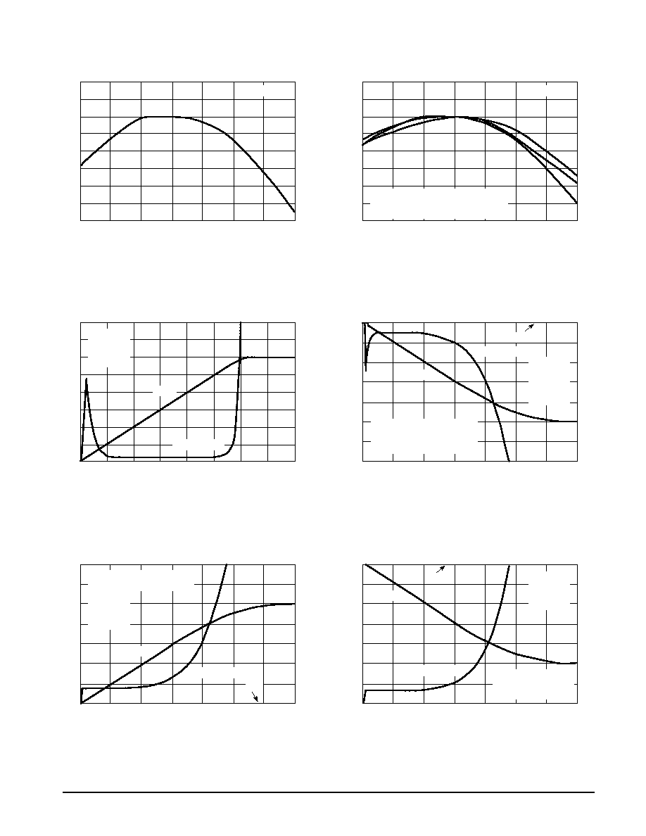
Figure 1. Voltage Sensing
Threshold Change versus Temperature
TA, AMBIENT TEMPERATURE (
∞
C)
Figure 2. Current Sensing
Threshold Change versus Temperature
VCC = 6.0 V
Figure 3. Closed≠Loop Voltage Sensing Input
versus Voltage Threshold Adjust
Figure 4. Closed≠Loop Current Sense Input B
versus Current Threshold Adjust
Figure 5. Closed≠Loop Current Sensing Input A
versus Current Threshold Adjust
Figure 6. Closed≠Loop Current Sensing Input A
versus Current Threshold Adjust
≠25
0
25
50
75
100
125
0.2
0.4
0.6
0.8
1.0
1.2
1.4
1.6
40
80
120
160
200
240
280
≠25
0
25
50
75
100
125
40
80
120
160
200
240
280
40
80
120
160
200
240
280
0
≠4.0
≠8.0
≠12
0
≠1.0
≠2.0
≠3.0
≠40
≠80
≠120
≠160
≠200
≠240
≠280
1.4
1.2
1.0
0.8
0.6
0.4
0.2
0
240
200
160
120
80
40
0
≠40
≠80
≠120
≠160
≠200
≠240
≠260
16
14
12
10
8.0
6.0
4.0
2.0
0
0
2.0
4.0
6.0
8.0
10
12
14
14
12
10
8.0
6.0
4.0
2.0
0
14
12
10
8.0
6.0
4.0
2.0
0
VCC = 6.0 V
1 ≠ Source High≠Side and Load High≠Side
2 ≠ Source Return Low≠Side
3 ≠ Load Low≠Side
VCC
VCC = 6.0 V
VO = 1.0 V
IO = 1.0 mA
TA = 25
∞
C
1
2
3
VPin 5
VPin 6≠VPin 5
VPin 6
VPin 1≠VPin 6
VCC = 6.0 V
VO = 1.0 V
IO = 1.0 mA
Pin 1 = VCC
TA = 25
∞
C
Gnd
VPin 5
VPin 2≠VPin 1
VCC = 6.0 V
VO = 1.0 V
IO = 1.0 mA
TA = 25
∞
C
VPin 2≠|VPin 1|
VPin 5
VCC = 6.0 V
VO = 1.0 V
IO = 1.0 mA
TA = 25
∞
C
Noninverting input path is active
for load low≠side current sensing.
Inverting Amplifier is
active for source return
low≠side current sensing.
Gnd
V
V
Pin 5
,
VOL
T
AGE SENSING INPUT
(V)
th(I HS)
, CURRENT
SENSING
V
th(v)
,
VOL
T
AGE
SENSING THRESHOLD CHANGE (mV)
THRESHOLD CHANGE (mV)
V
Pin 6
,
CURRENT
SENSE INPUT
B (mV)
V
Pin 1
,
CURRENT
SENSE INPUT
A
(mV)
V
Pin 2
≠V
Pin 1
, INPUT
DIFFERENCE VOL
T
AGE (mV)
V
Pin 1
,
CURRENT
SENSE INPUT
A
(mV)
V
Pin 6
≠V
Pin 5
, INPUT
DIFFERENCE VOL
T
AGE (mV)
V
Pin 1
≠V
Pin 6
, INPUT
DIFFERENCE VOL
T
AGE (mV)
V
Pin 2
≠|V
Pin 1
|, INPUT
DIFFERENCE VOL
T
AGE (mV)
Differential Amplifier is active for
source high≠side and load high≠side
current sensing. Both vertical axis are
expressed in millivolts down to VCC.

MC33341
5
MOTOROLA ANALOG IC DEVICE DATA
0
1.0
0.1
8.0
1.0 k
60
0
0
0.1
8.0
1.0 k
60
VCC, SUPPLY VOLTAGE (V)
IO, DRIVE OUTPUT LOAD CURRENT (mA)
f, FREQUENCY (Hz)
IL, OUTPUT LOAD CURRENT (mA)
IO, DRIVE OUTPUT LOAD CURRENT (mA)
Figure 7. Bode Plot
Voltage Sensing Inputs to Drive Output
f, FREQUENCY (Hz)
Figure 8. Bode Plot
Current Sensing Inputs to Drive Output
Figure 9. Transconductance
Voltage Sensing Inputs to Drive Output
Figure 10. Transconductance
Current Sensing Inputs to Drive Output
Figure 11. Drive Output High State
Source Saturation versus Load Current
Figure 12. Supply Current
versus Supply Voltage
VCC = 6.0 V
VO = 1.0 V
RL = 1.0 k
Pin 3 = 1.0 nF
TA = 25
∞
C
VCC = 6.0 V
VO = 1.0 V
RL = 1.0 k
Pin 3 = 1.8 nF
TA = 25
∞
C
VCC = 6.0 V
VO = 1.0 V
TA = 25
∞
C
VCC = 6.0 V
VO = 1.0 V
TA = 25
∞
C
VCC = 6.0 V
TA = 25
∞
C
IO = 0 mA
TA = 25
∞
C
Gain
Phase
Gain
Phase
High≠Side Sensing
Phase
Low≠Side Sensing
Drive Output Low State
10 k
10 k
100 k
1.0 M
100 k
1.0 M
0.2
0.3
0.5
1.0
2.0
3.0
5.0
10
0.2
0.3
0.5
1.0
2.0
3.0
5.0
10
4.0
8.0
12
16
20
4.0
8.0
12
16
50
40
30
20
10
0
50
40
30
20
10
0
6.0
4.0
2.0
0
6.0
4.0
2.0
0
≠0.4
≠0.8
≠1.2
≠1.6
≠2.0
0.8
0.6
0.4
0.2
0
180
160
140
120
100
80
180
160
140
120
100
80
A
VOL(I)
,
CURRENT
SENSING OPEN≠LOOP
, EXCESS PHASE (
∞
)
VOL
T
AGE GAIN (dB)
A
VOL(V)
,
VOL
T
AGE SENSING OPEN≠LOOP
VOL
T
AGE GAIN (dB)
g
m(v)
, VOL
T
AGE SENSING
TRANSCONDUCT
ANCE
(mhos)
g
m(I)
, CURRENT
SENSING TRANSCONDUCT
ANCE
(mhos)
V
OH
, OUTPUT
SOURCE SA
TURA
TION VOL
T
AGE (V)
, EXCESS PHASE (
∞
)
I CC
, SUPPL
Y
CURRENT
, DRIVE OUTPUT
LOW
ST
A
TE (mA)
VCC
Drive Output High State