 | –≠–ª–µ–∫—Ç—Ä–æ–Ω–Ω—ã–π –∫–æ–º–ø–æ–Ω–µ–Ω—Ç: MC33793D | –°–∫–∞—á–∞—Ç—å:  PDF PDF  ZIP ZIP |
Document Outline
- Introduction
- 33793 Simplified Application Diagram
- 33793 Simplified Internal Block Diagram
- Pin Function Description
- Maximum Ratings
- Static Electrical Characteristics
- Dynamic Electrical Characteristics
- Timing Diagrams
- System/Application Information
- Introduction
- Functional Description
- Operation
- DSI Commands and Responses
- Package Dimensions
MOTOROLA
SEMICONDUCTOR TECHNICAL DATA
© Motorola, Inc. 2003
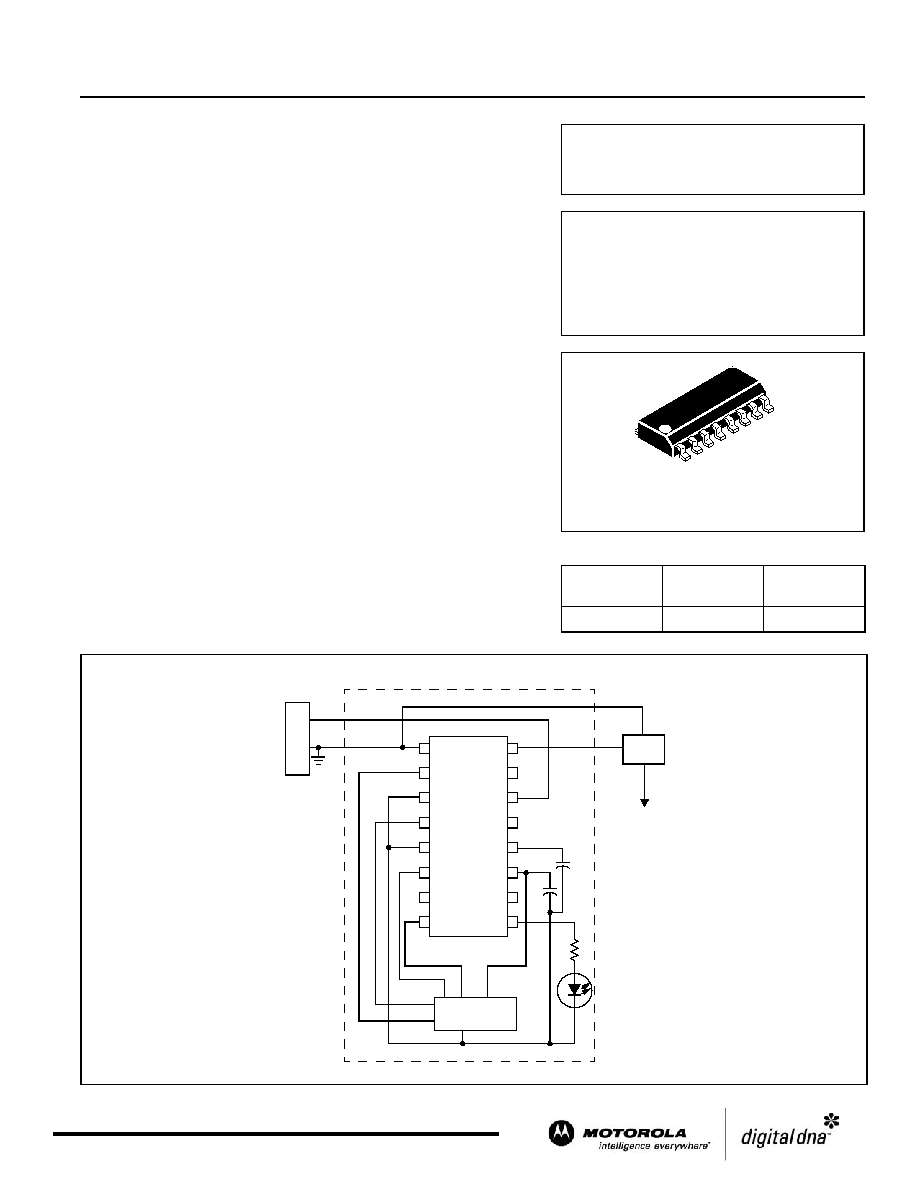
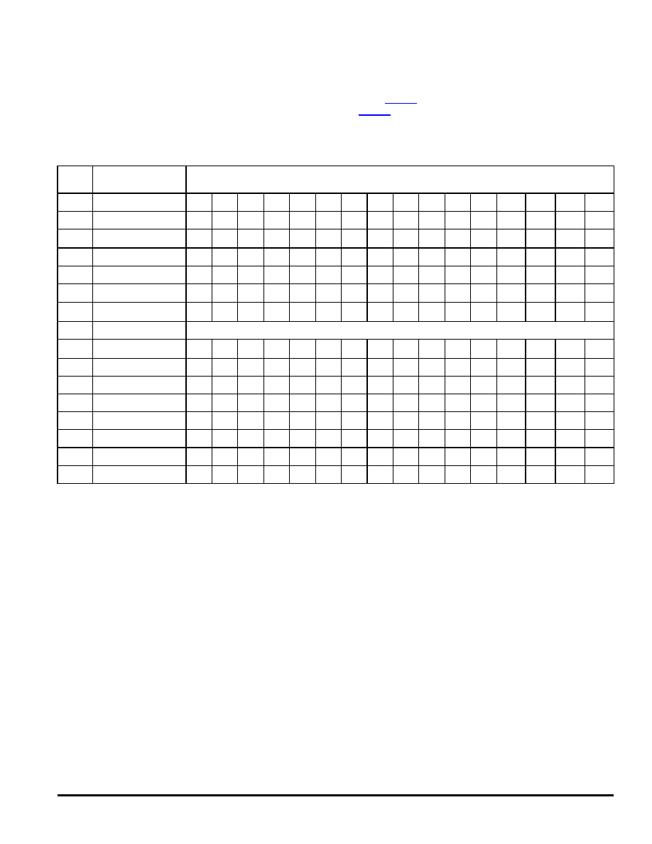
33793 Simplified Application Diagram
Document order number: MC33793/D
Rev 10, 07/2003
33793
Distributed System Interface (DSI)
Sensor Interface
The 33793 is a slave Distributed System Interface (DSI) device that is
optimized as a sensor interface. The device contains circuits to power sensors
such as accelerometers and to digitize the analog level from the sensor. The
device is controlled by commands over the DSI bus and returns measured
data over the bus.
Features
∑ 4-Channel, 8-Bit Analog-to-Digital Converter (ADC)
∑ 4 Pins Configurable as Analog or Logic Inputs or as Logic Outputs
∑ Provides Regulated +5.0 V Output for Sensor Power from Bus
∑ Additional High-Drive Logic Output
∑ Undervoltage Fault Detection and Signaling
∑ On-Board Clock (No External Elements Required)
∑ Field-Programmable Address
∑ Default and Field-Programmable as a DSI Daisy Chain Device
∑ Recognizes Reverse Initialization for Open Bus Fault Tolerance
∑ Detects Short to Battery on Bus Switch and Prevents Its Closure
DISTRIBUTED SYSTEM
INTERFACE (DSI) SENSOR
INTERFACE
BUSOUT
AGND
NC
BUSIN
NC
H_CAP
REGOUT
NC
LOGOUT
I/O1
AGND
I/O3
NC
I/O2
I/O0
BUSRTN
XY
ACCELEROMETER
TEST
ERROR
GND
V
CC
X
Y
1.0
µ
F
4.7
µ
F
DSIO
33793
To Other
DSI Slaves
BUSIN
BUSOUT
BUSRTN
33793
LED
1.0 K
33790
ORDERING INFORMATION
Device
Temperature
Range (T
J
)
Package
MC33793D/R2
-40∞C to 150∞C
16 SOICN
D SUFFIX
16-LEAD SOICN
CASE 751B
F
r
e
e
s
c
a
l
e
S
e
m
i
c
o
n
d
u
c
t
o
r
,
I
Freescale Semiconductor, Inc.
For More Information On This Product,
Go to: www.freescale.com
n
c
.
.
.
33793
MOTOROLA ANALOG INTEGRATED CIRCUIT DEVICE DATA
2
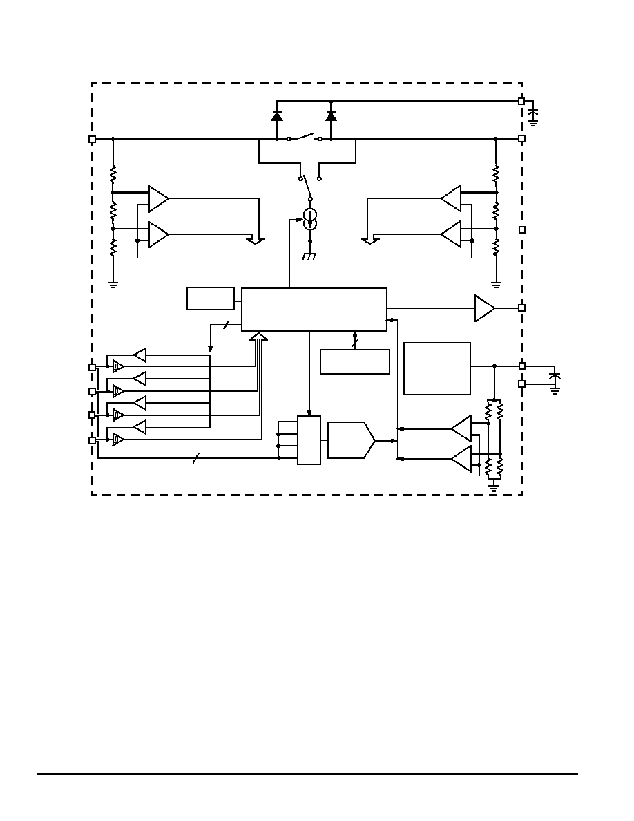
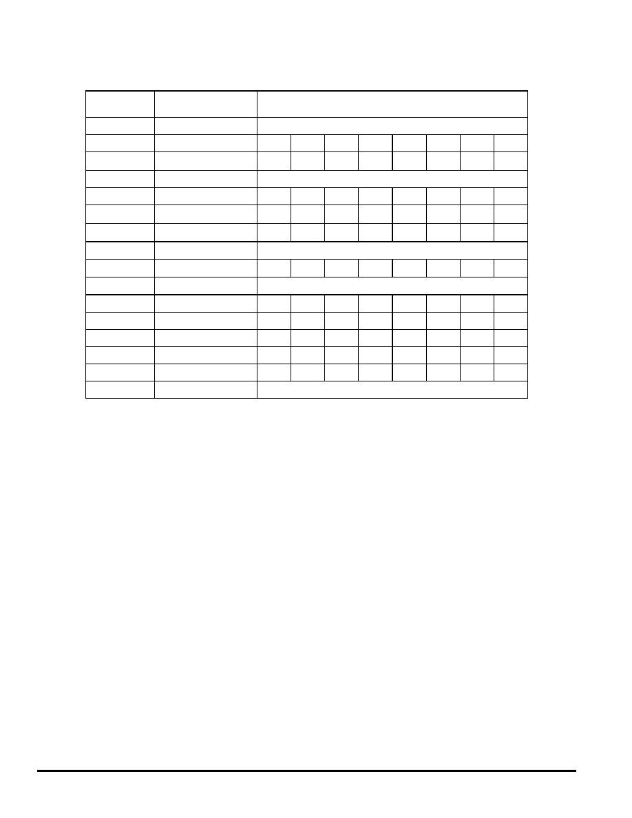
Figure 1. 33793 Simplified Internal Block Diagram
IO0
H_CAP
BUSOUT
BUSRTN
LOGOUT
REGOUT
IO1
IO2
IO3
BUSIN
Rectifiers
Bus Switch
0 ≠ 35 V Bi-Directional
Forward Receiver
Reverse Receiver
Data
Frame
Received
Message
from MCU
Bandgap
Reference
Data
Frame
Bandgap
Reference
1.0
µ
F
Typical
Response
Current
0 ≠11 mA
7.0 mA/
µ
S
Oscillator
4.0 MHz
Logic
Command Decode
State Machine
Response Generation
I/O Buffers
DataOut <3:0>
DataOut <0>
DataOut <1>
DataOut <2>
DataOut <3>
I/O<3:0>
I/O0
I/O1
I/O2
I/O3
SEL
Logic Out
High
Current
Buffer
Address A<3:0>
4 Bits NVM
Power
Management
5.0 V Regulator
BG Reference
Bias Currents
4:1
MUX
ADC
8 Bits
4
Supply Comparators
POR
Undervoltage
Detector
BG
GND
4.7
µ
F
Bus Return
F
r
e
e
s
c
a
l
e
S
e
m
i
c
o
n
d
u
c
t
o
r
,
I
Freescale Semiconductor, Inc.
For More Information On This Product,
Go to: www.freescale.com
n
c
.
.
.

MOTOROLA ANALOG INTEGRATED CIRCUIT DEVICE DATA
33793
3
PIN FUNCTION DESCRIPTION
Pin
Pin Name
Description
1
BUSRTN
This pin provides the common return for power and signalling.
2
I/O0
This pin can be used to provide a logic level output, a logic input, or an analog-to-digital (A/D) input.
3, 5
AGND
This pin is the low reference level and power return for the analog-to-digital converter (ADC).
4
I/O1
This pin can be used to provide a logic level output, a logic input, or an A/D input.
6
I/O3
This pin can be used to provide a logic level output, a logic input, or an A/D input.
7, 10, 13, 15
NC
These pins have no internal connections.
8
I/O2
This pin can be used to provide a logic level output, a logic input, or an A/D input.
9
LOGOUT
This is a logic output with higher pull-up drive capability than the standard logic I/O.
11
REGOUT
This pin provides a regulated 5.0 V output. The power is derived from the bus.
12
H_CAP
A capacitor attached to this pin is charged by the bus during bus idle and supplies current to run the device
and for external devices via the REGOUT pin during non-idle periods.
14
BUSIN
This pin attaches to the bus and responds to initialization commands.
16
BUSOUT
This pin attaches to the bus and responds to reverse initialization commands.
LOGOUT
BUSOUT
NC
BUSIN
NC
H_CAP
NC
REGOUT
I/O2
BUSRTN
I/O0
AGND
I/O1
AGND
NC
I/O3
8
2
3
4
5
7
6
9
16
15
14
13
12
10
11
1
F
r
e
e
s
c
a
l
e
S
e
m
i
c
o
n
d
u
c
t
o
r
,
I
Freescale Semiconductor, Inc.
For More Information On This Product,
Go to: www.freescale.com
n
c
.
.
.
33793
MOTOROLA ANALOG INTEGRATED CIRCUIT DEVICE DATA
4
MAXIMUM RATINGS
All voltages are with respect to ground unless otherwise noted.
Parameter
Symbol
Value
Unit
I/O Pin Voltage
V
IO
-0.3 to V
REGOUT
+ 0.5
V
I/O Pin Current
I
IO
5.0
mA
BUSIN, BUSOUT, BUSRTN, and H_CAP Voltage
V
IN
-0.3 to 40
V
BUSIN, BUSOUT, BUSRTN, and H_CAP Current (Continuous)
I
IN
250
mA
Storage Temperature
T
STG
-55 to 150
∞C
Operating Junction Temperature
T
J
-40 to 150
∞C
Lead Soldering Temperature (Note 1)
T
SOLDER
260
∞C
Thermal Resistance Junction to Case
R
JC
150
∞C/W
ESD Protection
Human Body Model (Note 2)
Machine Model (Note 3)
V
ESD1
V
ESD2
±2000
±200
V
Notes
1.
Lead soldering temperature limit is for 10 second maximum duration. Not designed for immersion soldering. Exceeding these limits may
cause malfunction or permanent damage to the device.
2.
ESD1 performed in accordance with the Human Body Model (C
ZAP
= 100 pF, R
ZAP
= 1500
).
3.
ESD2 performed in accordance with the Machine Model (C
ZAP
= 200 pF, R
ZAP
= 0
).
F
r
e
e
s
c
a
l
e
S
e
m
i
c
o
n
d
u
c
t
o
r
,
I
Freescale Semiconductor, Inc.
For More Information On This Product,
Go to: www.freescale.com
n
c
.
.
.

MOTOROLA ANALOG INTEGRATED CIRCUIT DEVICE DATA
33793
5
STATIC ELECTRICAL CHARACTERISTICS
Characteristics noted under conditions -0.3 V
V
BUSIN
or V
BUSOUT
30 V, 5.5 V < V
H_CAP
< 30 V, -40
∞C < T
J
< 150
∞C.
Parameter
Symbol
Min
Nom
Max
Units
Internal Quiescent Current Drain
V
H_CAP
= 25 V, Logout = 0, I/O = Input
I
Q
≠
≠
3.0
mA
BUSIN or BUSOUT to H_CAP Rectifier Voltage Drop
I
BUSIN
or I
BUSOUT
= 15 mA
I
BUSIN
or I
BUSOUT
= 100 mA
V
RECT
≠
≠
0.75
0.9
1.00
1.2
V
BUSIN + BUSOUT Bias Current
V
BUSIN
or V
BUSOUT
= 8.0 V, V
H_CAP
= 9.0 V
V
BUSIN
or V
BUSOUT
= 0.5 V, V
H_CAP
= 25 V
I
BIAS
-100
≠
≠
≠
100
20
µA
Rectifier Leakage Current
V
BUSIN
or V
BUSOUT
= 5.0 V, V
H_CAP
= 25 V
I
RLKG
-20
≠
100
µA
Reg0ut
5.5 V > V
H_CAP
> 25 V, I
RO
= 12 mA
V
REG
4.75
5.0
5.25
V
RegOut Line Regulation
I
RO
= 12 mA, 5.5 V > V
H_CAP
> 25 V
VR
LINE
≠
71
180
mV
RegOut Load Regulation
I
RO
= 0 to 12 mA, 5.5 V > V
H_CAP
> 25 V
VR
LD
≠
2.3
100
mV
Undervoltage Lockout
Proportional to unloaded V
REGOUT
V
UVL
0.93
0.95
0.97
V
RO
Bus Switch Resistance
V
BI
= 8.0 V, I
BO
= -80 mA (Bus Switch Active)
R
SW
≠
4.0
8.0
I/O0 and I/O3 Pull-Down Current
0 < V
BUSIN
or V
BUSOUT
< 1.0 V
I
PD
7.0
11
13
µA
I/O1 and I/O2 Pull-Up Current
V
RO
< V
BUSIN
or V
BUSOUT
< V
RO
- 1.0 V
I
PU
-7.0
-11
-13
µA
BUSIN and BUSOUT Logic Thresholds
Low
High
V
THL
V
THH
2.8
5.5
3.0
6.0
3.2
6.5
V
Logic Duty Cycle (assured by design)
Logic 0
Logic 1
D
CL
D
CH
10
60
33
67
40
90
%
BUSIN + BUSOUT Response Current
V
BUSIN
and/or
V
BUSOUT
= 4.0 V
I
RSP
9.9
11
12.1
mA
ADC Code Conversion Error (INL)
ADC
INL
≠
≠
< 1.0
LSB
ADC Full-scale Error
ADC
FS
≠
≠
3
counts
I/O Logic Input Thresholds
Logic High
Logic Low
V
IH
V
IL
0.7
≠
0.54
0.51
≠
0.3
V
RO
F
r
e
e
s
c
a
l
e
S
e
m
i
c
o
n
d
u
c
t
o
r
,
I
Freescale Semiconductor, Inc.
For More Information On This Product,
Go to: www.freescale.com
n
c
.
.
.
33793
MOTOROLA ANALOG INTEGRATED CIRCUIT DEVICE DATA
6
I/O Logic Output Levels
Output Low (I
L
= 1.0 mA)
Output High (I
L
= -500
µA)
V
OL
V
OH
0
0.8
0.08
0.985
0.5
1.0
V
V
RO
LOGOUT Output Levels
Output Low (I
L
= 500
µA)
Output High (I
L
= -10 mA, 6.2 V < V
H_CAP
< 25 V)
Output High (I
L
= -100
µA, 6.2 V < V
H_CAP
< 25 V)
V
LOL
V
LOH1
V
LOH2
0
4.7
≠
0.2
5.0
≠
0.5
5.3
V
RO
+0.5
V
Programming Time
From Positive Edge of BUSIN or BUSOUT > V
THH
on
Program Command to Following Command Negative
Transition < V
THH
T
PROG
100
200
1000
ms
NVM BUSIN or BUSOUT Programming Voltage
NVM
VP
22.25
≠
30
V
STATIC ELECTRICAL CHARACTERISTICS (continued)
Characteristics noted under conditions -0.3 V
V
BUSIN
or V
BUSOUT
30 V, 5.5 V < V
H_CAP
< 30 V, -40
∞C < T
J
< 150
∞C.
Parameter
Symbol
Min
Nom
Max
Units
F
r
e
e
s
c
a
l
e
S
e
m
i
c
o
n
d
u
c
t
o
r
,
I
Freescale Semiconductor, Inc.
For More Information On This Product,
Go to: www.freescale.com
n
c
.
.
.

MOTOROLA ANALOG INTEGRATED CIRCUIT DEVICE DATA
33793
7
DYNAMIC ELECTRICAL CHARACTERISTICS
Characteristics noted under conditions -0.3 V
V
BUSIN
or V
BUSOUT
30 V, 5.5 V
V
H_CAP
30 V, -40
∞C
T
J
150
∞C.
Characteristic
Symbol
Min
Typ
Max
Unit
Initialization to Bus Switch Closing
t
BS
100
150
200
µs
Loss of Signal Reset Time
Maximum Time Below Frame Threshold
t
TO
≠
≠
100
ms
ADC Code Conversion Time (Go, No-Go Test)
t
ADC
≠
≠
27
µs
BUSIN and BUSOUT Response Current Transition Time
1.0 mA to 9.0 mA Transition, 9.0 mA to 1.0 mA
t
ITR
≠
7.0
10
mA/
µs
BUSIN or BUSIN Timing to Response Current
BUSIN or BUSOUT Negative Voltage Transition = 3.0 V to I
RSPH
= 7.0 mA
BUSIN or BUSOUT Negative Voltage Transition = 3.0 V to I
RSPL
= 5.0 mA
t
RSPH
t
RSPL
≠
≠
≠
≠
3.3
3.3
µs
F
r
e
e
s
c
a
l
e
S
e
m
i
c
o
n
d
u
c
t
o
r
,
I
Freescale Semiconductor, Inc.
For More Information On This Product,
Go to: www.freescale.com
n
c
.
.
.

33793
MOTOROLA ANALOG INTEGRATED CIRCUIT DEVICE DATA
8
Timing Diagrams
Figure 2. Bus Switch and Reset Timing
Figure 3. Response Current Timing
t
BS
t
TO
BUSIN/BUSOUT
BUS Switch
Internal Reset
Open
Frame
Threshold
Frame
Threshold
Closed
End of Initialization
Command
Reset
9.0 mA
7.0 mA
1.0 mA
1.0 mA
5.0 mA
9.0 mA
t
ITR
t
ITR
t
RSPL
t
RSPH
3.0 V
3.0 V
BUSIN/BUSOUT
RESPONSE
CURRENT
F
r
e
e
s
c
a
l
e
S
e
m
i
c
o
n
d
u
c
t
o
r
,
I
Freescale Semiconductor, Inc.
For More Information On This Product,
Go to: www.freescale.com
n
c
.
.
.

MOTOROLA ANALOG INTEGRATED CIRCUIT DEVICE DATA
33793
9
SYSTEM/APPLICATION INFORMATION
INTRODUCTION
The 33793 is designed to be used with a sensor at a location
that is remote from a centralized MCU. This device provides
power, measurement, and communications between the
remote sensor and the centralized MCU over a DSI bus.
Sensors such as accelerometers can be powered from the
regulated output of the device, and the resulting analog value
from the sensor can be converted from an analog level to a
digital value for transmission over the DSI bus in response to a
query from the MCU. Four I/O lines can be configured by the
central MCU over the DSI bus as analog inputs, digital inputs,
or digital outputs. This allows more than one sensor to be
remotely controlled and measured by a single 33793.
Additionally, a high drive logic output is provided that can be
used to power other low-power sensors.
Power is passed from BUSIN or BUSOUT through on-board
rectifiers to a storage capacitor (referred to as the H_CAP). The
H_CAP stores energy during the highest voltage excursions of
the BUSIN or BUSOUT pin (idle) and supplies energy to power
the device during low excursions of BUSIN and BUSOUT.
The Regulator supplies an on-board regulated voltage for
internal use, and the Power on Reset (POR) circuit provides a
reset signal during low-voltage conditions and during power up/
down. Some current is available for low-power sensors.
Data from the Central Control Unit (CCU) is applied to the
BUSIN and/or BUSOUT pins as voltage levels that are sensed
by the Level Detection circuitry. The Serial Decoder detects
these transitions and decodes the incoming data. The Control
Logic provides overall control of the 33793. It controls
diagnostic testing and formats responses to commands with the
message encoder. Responses are formed via a switched
current source that is slew-rate controlled.
The one-time programmable (OTP) memory array provides
the nonvolatile storage for the pre-programmed address. It is
accessed via the Read/Write NVM command. It has a built-in
hardware lock that only allows one write.
FUNCTIONAL DESCRIPTION
Refer to
Figure 1
, 33793 Internal Block Diagram, page 2, for
a simplified representation of the 33793's components.
Rectifier
This rectifier or switch peak detects the bus signal into an
external capacitor attached to H_CAP. The capacitor supplies
power during signaling while the input voltage is at a lower level.
The voltage waveform at BUSIN and/or BUSOUT and the
size of the filter capacitor at H_CAP must be such that the
voltage at H_CAP will not drop below the frame threshold
during signaling.
POR
The 33793 leaves the reset state when the voltage on
H_CAP rises above the Power-ON Reset threshold.
Timeout
A timeout timer keeps track of the length of the time when the
input is not in idle mode. If this time exceeds a limit, the part is
reset. The purpose of this is to allow the part to reset itself if the
connection to the master is lost or if power is removed from the
system.
5.0 V Regulator
The 5.0 V regulator supplies internal power for the device
and also provides approximately 6.0 mA through the REGOUT
pin to power an external sensor.
Undervoltage Detector
The undervoltage detector monitors the output voltage of the
5.0 V regulator. If the REGOUT voltage drops too low for
accurate A/D operation, a signal is sent to the control logic. The
control logic will interpret this signal and, in response to a
command, report a status indicating an undervoltage condition
to have existed. When received, the command will clear the
signal after having read the status. If the voltage is too low when
the A/D conversion was completed, the returned value will be
zero (binary 00000000).
IO Pins 0 to 3
The IO pins can serve as logic inputs, logic outputs, or
analog inputs. At power-up or after a clear, the pins are all logic
inputs and can be used to measure an analog level value for an
analog value request command. The pins can be individually
configured as logic inputs or outputs by the IO Control
command. If the pin is configured as a logic output, reading the
analog value will return the analog level the output is being
driven to.
Analog-to-Digital Converter
The ADC is an 8-bit successive approximation type using on-
board capacitive division. It uses the Clk signal from the on-
board oscillator for sequencing.
The ADC uses REGOUT as a full-scale reference voltage
and ground AGND for a zero-level reference.
The ADC signals when it has made a valid conversion by
asserting a signal to the controller. If this signal is not asserted
F
r
e
e
s
c
a
l
e
S
e
m
i
c
o
n
d
u
c
t
o
r
,
I
Freescale Semiconductor, Inc.
For More Information On This Product,
Go to: www.freescale.com
n
c
.
.
.

33793
MOTOROLA ANALOG INTEGRATED CIRCUIT DEVICE DATA
10
when a value is being captured by the controller, the controller
will signal that an invalid A/D value was obtained.
The value of "0" (binary 00000000) is reserved by the control
logic to signal an error. A value of "0" from the ADC will be
reported as "1" (binary 00000001) by the control logic.
Serial Encoder
The Serial Encoder accepts the digitized value from the ADC
and formatting/data from the Control Logic. A logic transition
from Idle to Signal High and then to Signal Low at BUSIN will
cause the first bit to be presented to the current switch
(Response Loading). A transition to Signal High and back to
Signal Low will cause the next bit to be presented to the current
switch. This will continue until a transition back to Idle turns off
the current switch.
Slew
The slew circuit serves to reduce EMI produced as a result
of switching the bus loading current sink element. The slew
circuit limits the rise and fall time of current loading the bus by
controlling the current sinking element.
Switched Current Source
A "1" data return bit will be signaled by turning on a fixed
current source. During signaling time, the 33793 will be using
power from H_CAP and not loading the bus for power. The
current will be drawn from either BUSIN or BUSOUT or split
between them. The split can be in any proportion as long as the
total is correct.
The current source is turned off whenever the bus is at Idle
level.
Level Detector
The level detector contains comparators to determine if the
BUSIN or BUSOUT is at idle, logic high, or logic low. The inputs
from BUSIN and BUSOUT are sensed by the device so that if
either side is driven by the signaling waveform while the other
is not, the signaling will be detected. This circuit also provides a
signal to indicate if the signal is being received on the BUSOUT
pin. If a "reverse initialization" command is received, it can only
be acted upon if the device is not already initialized and if the
signal is present on BUSOUT.
Serial Decoder
The Serial Decoder monitors transitions on the BUSIN or
BUSOUT. When the 33793 is Idle and supplying power to itself
and the external device(s) (via REGOUT), the input to BUSIN
will be in the Idle state. A transition from this level to Signal Low
(through Signal High) will start the process of decoding a word
of data. BUSIN is driven from Signal Low to Signal High for each
bit and back to Signal Low to start the next bit. The
determination of whether the bit was a one or a zero is made by
determining whether it spent more time low (a zero) or high (a
one). The end of the word is signaled by a transition at the end
of the last bit from Signal High to Idle. The advantage of this
method is that it will accept data over a wide range of rates and
is not dependent on an accurate clock.
The controller will typically indicate a logic zero by spending
2/3 of the bit period at Signal Low and 1/3 at Signal High. A logic
one would be 1/3 of the bit period at Signal Low and 2/3 at
Signal High.
Control Logic
The control logic performs the digital operations carried out
by this device. Its principle functions include:
∑ Decoding input instructions.
∑ Control the general purpose I/O and LOGICOUT in
response to BUSIN or BUSOUT commands.
∑ Control A/D conversions.
∑ Form response word.
∑ Capture and store address.
∑ Control BUSSW.
∑ Reset device on power-up.
∑ Control the general purpose I/O logic configuration.
∑ Read the general purpose I/O logic values and respond to
request for these values.
∑ Generating a cycle redundancy check (CRC) for the
received data and transmitted data in conformance with
the DSI Bus Standard.
Additionally, the control logic performs error checking on the
received data. If errors are found, no action is taken and no
response is made. Errors include:
∑ CRC received doesn't match CRC of received data.
∑ Number of received bits is not 12 or 20.
Clock
The clock is a low-stability type with the capacitor integrated
onto the die. The signaling system and all internal operations
are such that no external precision timing device is needed in
the normal operation of this device.
Bus Switch (BUSSW)
The bus switch passes signaling and power to all
subsequent devices on the bus. It can block a voltage of either
polarity up to the highest idle state level between BUSIN and
BUSOUT.
LOGICOUT
LOGICOUT is a logic level output with enhanced high-side
drive capability.
Addressing
The 33793 IC supports both runtime programmable and pre-
programmed addressing as defined in the DSI Specification.
Runtime programmable addressing uses the daisy chain bus
connection. Pre-programmed devices may either be connected
in daisy chain or in parallel on the bus wires.
F
r
e
e
s
c
a
l
e
S
e
m
i
c
o
n
d
u
c
t
o
r
,
I
Freescale Semiconductor, Inc.
For More Information On This Product,
Go to: www.freescale.com
n
c
.
.
.

MOTOROLA ANALOG INTEGRATED CIRCUIT DEVICE DATA
33793
11
Programmable address devices all power up with a device
address of $0 in their address register and their bus switches
open. In the daisy chain, if the first device receives the
initialization command device on BUSIN, it will accept the
address in the command and close its switch at the end of the
command. The next device in the chain will now be able to
receive the initialization command on its BUSIN and will accept
the next address. This proceeds down the chain until the last
device is addressed. The devices can also be initialized by the
reverse initialization command if the signal is applied to
BUSOUT.
Pre-programmed devices power up with their pre-
programmed address in its address register. It will ignore all
Initialization commands unless the address in the command
matches its pre-programmed address. In this event the device
stores the other information contained in the Initialization
command.
F
r
e
e
s
c
a
l
e
S
e
m
i
c
o
n
d
u
c
t
o
r
,
I
Freescale Semiconductor, Inc.
For More Information On This Product,
Go to: www.freescale.com
n
c
.
.
.

33793
MOTOROLA ANALOG INTEGRATED CIRCUIT DEVICE DATA
12
OPERATION
A device may be permanently programmed one time with an
address using a two-command sequence. The first step is
satisfied on the reception of an Initialization command with
address set to zero, the PA[3:0] set to the address to be
programmed, and the NV bit set. This will cause the address
contained in the PA[3:0] bits to be stored in the address register
and the bus switch closed. The second step is taken when a
Read/Write NVM command is received with the PA[3:0] bits
matching the A[3:0] bits and also matching the bits stored in the
33793 address register. This will cause the 33793 to
permanently store this address into an internal NVM area.
Messages
The messages follow the format defined in the Distributed
Systems Interface Specification rev 1.0 unless otherwise noted.
DSI Bus Commands
This device can recognize and respond to both long-word
and short-word commands. A command word summary is
shown in
Table 1
. SW in the "Size" column of the table indicates
short-word commands and LW indicates long-word commands.
Short-word commands may also be sent in the long-word
format. However, when these commands are sent in the long-
word format, it is recommended that the data byte be sent as
$00 to maintain future compatibility. All commands marked
reserved should not be sent to 33793 slaves.
Table 1. DSI Bus Commands
Command
Size
Description
Data
C3
C2
C1
C0
D7
D6
D5
D4
D3
D2
D1
D0
0
0
0
0
LW
Initialization
NV
BS
G1
G0
PA3
PA2
PA1
PA0
0
0
0
1
SW
Request Status
≠
≠
≠
≠
≠
≠
≠
≠
0
0
1
0
SW
Request Value 0
≠
≠
≠
≠
≠
≠
≠
≠
0
0
1
1
LW
I/O Control
L3
L2
L1
L0
DR3
DR2
DR1
DR0
0
1
0
0
SW
Request ID Information
≠
≠
≠
≠
≠
≠
≠
≠
0
1
0
1
SW
Request Value 1
≠
≠
≠
≠
≠
≠
≠
≠
0
1
1
0
SW
Request Value 2
≠
≠
≠
≠
≠
≠
≠
≠
0
1
1
1
SW
Clear
≠
≠
≠
≠
≠
≠
≠
≠
1
0
0
0
SW
Request Value 3
≠
≠
≠
≠
≠
≠
≠
≠
1
0
0
1
LW
Read/Write NVM
1
1
1
1
PA3
PA2
PA1
PA0
1
0
1
0
Reserved
1
0
1
1
Reserved
1
1
0
0
SW
Clear Logic Out
≠
≠
≠
≠
≠
≠
≠
≠
1
1
0
1
SW
Set Logic Out
≠
≠
≠
≠
≠
≠
≠
≠
1
1
1
0
Reserved
1
1
1
1
LW
Reverse Initialization
NV
BS
G1
G0
PA3
PA2
PA1
PA0
Legend
BS = Controls closing of the Bus Switch (1 = close).
DR[3:0] = Direction of I/O. 1 = Output.
G[1:0] = Group assignment (the 33793 does not use these bits).
L[3:0] = Level to output on I/O if configured as outputs.
LO = Logic Out level.
PA[3:0] = Bus Address to set the device to.
NV = Allows nonvolatile address programming if set to "1".
F
r
e
e
s
c
a
l
e
S
e
m
i
c
o
n
d
u
c
t
o
r
,
I
Freescale Semiconductor, Inc.
For More Information On This Product,
Go to: www.freescale.com
n
c
.
.
.
MOTOROLA ANALOG INTEGRATED CIRCUIT DEVICE DATA
33793
13
Long- and Short-Word Responses
The device responds to long-word commands with long-word
responses and short-word commands with short-word
responses. Responses are sent during the next message
following the command. A long-word response summary is
found in
Table 2
and a short-word response summary is found
in
Table 3
, page 14.
Table 2. Long-Word Response Summary
CMD
hex
Command
Description
Response
0
Initialization
A3
A2
A1
A0
0
0
0
BF
NV
BS
G1
G0
PA3
PA2
PA1
PA0
1
Request Status
A3
A2
A1
A0
0
0
0
0
NV
U
LO
BS
IO3
IO2
IO1
IO0
2
Request Value
0
A3
A2
A1
A0
0
0
0
0
B7
B6
B5
B4
B3
B2
B1
B0
3
I/O Control
A3
A2
A1
A0
0
0
0
0
L3
L2
L1
L0
DR3
DR2
DR1
DR0
4
Request ID
A3
A2
A1
A0
0
0
0
0
V2
V1
V0
0
0
0
1
1
5
Request Value
1
A3
A2
A1
A0
0
0
0
0
B7
B6
B5
B4
B3
B2
B1
B0
6
Request Value
2
A3
A2
A1
A0
0
0
0
0
B7
B6
B5
B4
B3
B2
B1
B0
7
Clear
No Response
8
Request Value
3
A3
A2
A1
A0
0
0
0
0
B7
B6
B5
B4
B3
B2
B1
B0
9
Read/Write NVM
A3
A2
A1
A0
0
0
0
0
1
1
1
1
PA3
PA2
PA1
PA0
A
Reserved
B
Reserved
C
Clear Logic Out
A3
A2
A1
A0
0
0
0
0
NV
U
LO
BS
IO3
IO2
IO1
IO0
D
Set Logic Out
A3
A2
A1
A0
0
0
0
0
NV
U
LO
BS
IO3
IO2
IO1
IO0
E
Reserved
F
Reverse Initialization
A3
A2
A1
A0
0
0
0
BF
NV
BS
G1
G0
PA3
PA2
PA1
PA0
Legend
A[3:0] = Address bits. The slave address.
B[7:0] = 8-bit A/D value.
BF = Bus Fault
BS = Status of the Bus Switch (1 = close).
DR[3:0] = I/O direction bits (1 = Output).
G[1:0] = Group assignment (the 33793 does not use these bits).
IO[3:0] = Logic level of I/O.
L[3:0] = Level to output on I/O if configured as outputs.
LO = Logic Out level at the Logic Out pin.
NV = Allows nonvolatile address programming if set to "1".
PA[3:0] = Bus Address to set the device to.
U = Undervoltage Flag.
V[2:0] = Version number.
F
r
e
e
s
c
a
l
e
S
e
m
i
c
o
n
d
u
c
t
o
r
,
I
Freescale Semiconductor, Inc.
For More Information On This Product,
Go to: www.freescale.com
n
c
.
.
.
33793
MOTOROLA ANALOG INTEGRATED CIRCUIT DEVICE DATA
14
Table 3. Short-Word Response Summary
Command
Command
Description
Response
0000
Initialization
Not Valid
0001
Request Status
NV
U
LO
BS
IO3
IO2
IO1
IO0
0010
Request Value
0
B7
B6
B5
B4
B3
B2
B1
B0
0011
I/O Control
Not Valid
0100
Request ID Information
V2
V1
V0
0
0
0
1
1
0101
Request Value
1
B7
B6
B5
B4
B3
B2
B1
B0
0110
Request Value
2
B7
B6
B5
B4
B3
B2
B1
B0
0111
Clear
No Response
1000
Request Value
3
B7
B6
B5
B4
B3
B2
B1
B0
1001
Read/Write NVM
Not Valid
1010
Reserved
1011
Reserved
1100
Clear Logic Out
NV
U
LO
BS
IO3
IO2
IO1
IO0
1101
Set Logic Out
NV
U
LO
BS
IO3
IO2
IO1
IO0
1110
Reserved
1111
Reverse Initialization
Not Valid
Legend
B[7:0] = 8-bit A/D value.
BS = Status of the Bus Switch (1 = close).
LO = Logic Out level at the Logic Out pin.
IO[3:0] = Logic level of I/O.
NV = Allows nonvolatile address programming if set to "1".
PA[3:0] = Bus Address to set the device to.
U = Undervoltage Flag.
V[2:0] = Version number.
F
r
e
e
s
c
a
l
e
S
e
m
i
c
o
n
d
u
c
t
o
r
,
I
Freescale Semiconductor, Inc.
For More Information On This Product,
Go to: www.freescale.com
n
c
.
.
.

MOTOROLA ANALOG INTEGRATED CIRCUIT DEVICE DATA
33793
15
DSI COMMANDS AND RESPONSES
Initialization Command
The Initialization command must be sent to the 33793 before
it may commence communications over the bus. The command
may be used three ways. The first is to initialize a
programmable address device. The second is the first step in
assigning a pre-programmed address. The third is to initialize a
pre-programmed device.
For the first case this command is sent to address zero with
the NV bit set to zero. The command will be received by the next
daisy chain device with its bus switch open. Reception of this
command will assign the device address and group number.
For the second case the Initialization command is sent the
same as the first except that the NV bit is set to one. Reception
of the command will assign the device address and group
number. A Read/Write NVM command then may be sent to
complete the setting of a pre-programmed address.
A pre-programmed device must be initialized by putting its
address in both PA3:PA0 and A3:A0 fields.
Once a device has received an initialization command, it will
ignore further initialization commands unless it has received a
Clear command or undergone a power-up reset.
If BS = 1 and no faults are detected, initialization will cause
the bus switch to close.
The command format is found in
Table 4
.
Initialization Response
This response message is sent during the next message
following a valid Initialization command to the addressed
device. The response is shown in
Table 5
. Because this is a
long-word only command, the short-word response is invalid.
Request Status Command
This command will cause the addressed device to return the
status of the NV, U, and BS bits and the logic levels of the I/O
and LOGICOUT. The command format is found in
Table 6
.
Table 4. Initialization Command Format
Data
Address
Command
CRC
NV
BS
G1
G0
PA3
PA2
PA1
PA0
A3
A2
A1
A0
0
0
0
0
X3
X2
X1
X0
Legend
A[3:0] = Address bits. The slave address.
BS = Bus Switch Position (1 = closed).
G[1:0] = Group bits (unused).
NV = Nonvolatile Memory Write. The value of the NV bit in the slave.
PA[3:0] = Bus Address to set the device to.
X[3:0] = Cyclic Redundancy Check (CRC). The CRC as calculated by the
master.
Table 5. Initialization Response Format
High Byte
Low Byte
CRC
A3
A2
A1
A0
0
0
0
BF
NV
BS
G1
G0
PA3
PA2
PA1
PA0
X3
X2
X1
X0
Legend
A[3:0] = Address bits. The slave address.
BF = Bus Fault. Bus out short to battery detected.
BS = Bus Switch Position (1 = closed).
G[1:0] = Group bits (unused).
NV = Nonvolatile Memory Write. The value of the NV bit in the slave.
PA[3:0] = Bus Address to set the device to.
X[3:0] = Cyclic Redundancy Check (CRC). The CRC as calculated by
the slave.
Table 6. Request Status Command Format
Data
Address
Command
CRC
≠
≠
≠
≠
≠
≠
≠
≠
A3
A2
A1
A0
0
0
0
1
X3
X2
X1
X0
Legend
A[3:0] = Address bits. The address of the selected device. An
address value of "0000" is ignored by all devices.
X[3:0] = Cyclic Redundancy Check (CRC). The CRC as calculated
by the master.
F
r
e
e
s
c
a
l
e
S
e
m
i
c
o
n
d
u
c
t
o
r
,
I
Freescale Semiconductor, Inc.
For More Information On This Product,
Go to: www.freescale.com
n
c
.
.
.
33793
MOTOROLA ANALOG INTEGRATED CIRCUIT DEVICE DATA
16
Request Status Response
This response message is sent during the next message
following a valid Request Status command to the addressed
device. The response format is found in
Table 7
. The high byte
is omitted during the short-word response. No response is
generated if the command address field was $0.
Request Value n Command
This command will cause the analog level at one of the four
I/O lines to be measured and returned on the following
command. The command format is found in
Table 8
. The
analog input measured is defined in
Table 9
.
Request Values Response
This response is an 8-bit value representing the value
measured by the ADC. The selection of "n" is a function of the
command. This is shown in
Table 10
.
The read will be completed during the idle period and will
represent the voltage at the end of the command. If an
undervoltage condition exists at any time during the command
or the measurement has not completed properly, a value of
"00000000" will be returned. This is a reserved value to indicate
a problem with the measurement. The minimum valid level
reported will be "00000001". No response is generated if the
command address field was $0.
Table 7. Request Status Response Format
High Byte
Low Byte
CRC
A3
A2
A1
A0
0
0
0
0
NV
U
LO
BS
IO3
IO2
IO1
IO0
X3
X2
X1
X0
Legend
A[3:0] = Address bits. The slave address.
BS = Bus Switch Position (1 = closed).
LO = Logic out driven level.
IO[3:0] = Values at logic I/Os.
NV = Nonvolatile Memory Write. The value of the NV bit in the slave.
U = Undervoltage indicated true by a "1".
X[3:0] = Cyclic Redundancy Check (CRC). The CRC as calculated by
the slave.
Table 8. Request Value n Command Format
Data
Address
Command
CRC
≠
≠
≠
≠
≠
≠
≠
≠
A3
A2
A1
A0
C3
C2
C1
C0
X3
X2
X1
X0
Legend
A[3:0] = Address bits. The address of the selected device.
An address value of "0000" is ignored by all devices.
C[3:0] = Command number.
X[3:0] = Cyclic Redundancy Check (CRC). The CRC as calculated
by the master.
Table 9. Analog Input Selection
Command
A/D Input
0010
I/O0
0101
I/O1
0110
I/O2
1000
I/O3
Table 10. Request Values Response Format
High Byte
Low Byte
CRC
A3
A2
A1
A0
0
0
0
0
D7
D6
D5
D4
D3
D2
D1
D0
X3
X2
X1
X0
Legend
A[3:0] = Address bits. The address of the selected device.
An address value of "0000" is ignored by all devices.
D[7:0] = Measured value (MSB = D7).
X[3:0] = Cyclic Redundancy Check (CRC).
F
r
e
e
s
c
a
l
e
S
e
m
i
c
o
n
d
u
c
t
o
r
,
I
Freescale Semiconductor, Inc.
For More Information On This Product,
Go to: www.freescale.com
n
c
.
.
.

MOTOROLA ANALOG INTEGRATED CIRCUIT DEVICE DATA
33793
17
I/O Control Command
This register controls the I/O ports. When the "DR" bits are
set, the corresponding I/O is enabled as an output. The "L" bit
settings control the level of the corresponding I/O if it is enabled
as an output. The format of this command is shown in
Table 11
.
I/O Control Response
The response indicates which I/O has been configured as
outputs and their current values.
The values returned will be the values programmed. The
values at the pins will not be the ones that were programmed if
the pin has been forced to the opposite state. The response
format is shown in
Table 12
. No response is generated if the
command address field was $0.
Request ID Command
This command will cause the device ID information to be
read from internal storage and returned to the master during the
response to the next message. The command format is found
in
Table 13
.
Table 11. I/O Control Command Format
Data
Address
Command
CRC
L3
L2
L1
L0
DR3
DR2
DR1
DR0
A3
A2
A1
A0
0
0
1
1
X3
X2
X1
X0
Legend
A[3:0] = Address bits.
DR[3:0] = I/O direction bits. 1 = Output. All bits are set to "0"
by reset/clear.
L[3:0] = Level to output on I/O if configured as output. All bits are set
to "0" by reset/clear
X[3:0] = Cyclic Redundancy Check (CRC). The CRC as calculated
by the master.
Table 12. I/O Control Response Format
High Byte
Low Byte
CRC
A3
A2
A1
A0
0
0
0
0
L3
L2
L1
L0
DR3
DR2
DR1
DR0
X3
X2
X1
X0
Legend
A[3:0] = Address bits.
DR[3:0] = I/O enabled as outputs (1 = enabled as output).
L[3:0] = Programmed values.
X[3:0] = Cyclic Redundancy Check (CRC). The CRC as calculated by
the slave.
Table 13. Request ID Command Format
Data
Address
Command
CRC
≠
≠
≠
≠
≠
≠
≠
≠
A3
A2
A1
A0
0
1
0
0
X3
X2
X1
X0
Legend
A[3:0] = Address bits. The address of the selected device.
An address value of "0000" is ignored by all devices.
X[3:0] = Cyclic Redundancy Check (CRC). The CRC as calculated
by the master.
F
r
e
e
s
c
a
l
e
S
e
m
i
c
o
n
d
u
c
t
o
r
,
I
Freescale Semiconductor, Inc.
For More Information On This Product,
Go to: www.freescale.com
n
c
.
.
.

33793
MOTOROLA ANALOG INTEGRATED CIRCUIT DEVICE DATA
18
Request ID Response
This response message is sent during the next message
following a valid long-word Request ID command to the
addressed device. The response format is found in
Table 14
.
The high byte is omitted during the short-word response. No
response is generated if the command address field was $0.
Clear Command
This command will open the bus switch and reset all
registers to the reset state. The command format is found in
Table 15
. No response is generated for the Clear command.
Read/Write NVM Command
If the NV bit has been set by a previous Initialization
command and the NVM has not been programmed previously,
this command will permanently program the device's one-time
programmable address and return the programmed value
during the next message time. Once programmed, this
nonvolatile address is used to set the device address register
on the next and all subsequent power-ups. If the device is not
blank, this command will return the programmed value during
the next message time.
Programming the NVM address to $0 is allowed. This
ensures that the device always acts as a dynamically
addressable device and would be immune to any inadvertent
future NVM programming sequences.
Reads and writes are long-word commands only. The
command format is found in
Table 16
.
Table 14. Request ID Response Format
Address
Status
Data
CRC
A3
A2
A1
A0
0
0
0
0
V2
V1
V0
0
0
0
1
1
X3
X2
X1
X0
Legend
A[3:0] = Address bits. The slave address.
V[2:0] = Device version number. The silicon version number of
the device. For this device the device type is 00011 as indicated
by the lowest bits.
X[3:0] = Cyclic Redundancy Check (CRC). The CRC as calculated by
the slave.
Table 15. Clear Command Format
Data
Address
Command
CRC
≠
≠
≠
≠
≠
≠
≠
≠
A3
A2
A1
A0
0
1
1
1
X3
X2
X1
X0
Legend
A[3:0] = Address bits. The address of the selected device.
An address value of "0000" clears all devices.
X[3:0] = Cyclic Redundancy Check (CRC). The CRC as calculated
by the master.
Table 16. Read/Write NVM Command Format
Data
Address
Command
CRC
1
1
1
1
PA3
PA2
PA1
PA0
A3
A2
A1
A0
1
0
0
1
X3
X2
X1
X0
Legend
A[3:0] = Address bits. These bits are the address of the
device previously sent with the Initialization command. They
must match the address in the PA[3:0] field and the address
stored in the device address register.
PA[3:0] = Program Address bits. These bits are the address that is
to be programmed into the slave.
X[3:0] = Cyclic Redundancy Check (CRC). The CRC as calculated
by the master.
F
r
e
e
s
c
a
l
e
S
e
m
i
c
o
n
d
u
c
t
o
r
,
I
Freescale Semiconductor, Inc.
For More Information On This Product,
Go to: www.freescale.com
n
c
.
.
.

MOTOROLA ANALOG INTEGRATED CIRCUIT DEVICE DATA
33793
19
Read/Write NVM Response
This response message is sent during the next message
following a valid Read/Write NVM command to the addressed
device. The response format is found in
Table 17
. The high byte
is omitted during the short-word response. No response is
generated if the command address field was $0.
Clear Logic Out Command
The Clear Logic Out command sets the Logic Out pin to a
logic low. The compliment to this command is the Set Logic Out.
The Logic Out is also cleared at power-up or following a Clear
command. The format of the Clear Logic Out command is
shown in
Table 18
.
Clear Logic Out Response
This response message is sent during the next message
following a valid Clear Logic Out command to the addressed
device. The response is shown in
Table 19
. No response is
generated if the command address field was $0.
Set Logic Out Command
The Set Logic Out command sets the Logic Out pin to a logic
high. The compliment to this command is the Clear Logic Out.
The Logic Out is cleared at power-up or following a Clear
command. The format of the Clear Logic Out command is
shown in
Table 20
.
Table 17. Read/Write NVM Response Format
High Byte
Low Byte
CRC
A3
A2
A1
A0
0
0
0
0
1
1
1
1
PA3
PA2
PA1
PA0
X3
X2
X1
X0
Legend
A[3:0] = Address bits. The slave address.
PA[3:0] = Programmed Address bits. The address that was
programmed into the NVM address bits of the slave.
X[3:0] = Cyclic Redundancy Check (CRC). The CRC as calculated by
the slave.
Table 18. Clear Logic Out Command Format
Data
Address
Command
CRC
≠
≠
≠
≠
≠
≠
≠
≠-
A3
A2
A1
A0
1
1
0
0
X3
X2
X1
X0
Legend
A[3:0] = Address bits. The address of the selected
device.
X[3:0] = Cyclic Redundancy Check (CRC). The CRC as calculated
by the master.
Table 19. Clear Logic Out Response Format
High Byte
Low Byte
CRC
A3
A2
A1
A0
0
0
0
0
NV
U
LO
BS
IO3
IO2
IO1
IO0
X3
X2
X1
X0
Legend
A[3:0] = Address bits. The slave address.
BS = Bus Switch Position (1=closed).
LO = Logic out driven level.
IO[3:0] = Values at logic I/Os.
NV = Nonvolatile Memory Write. The value of the NV bit in the slave.
U = Undervoltage indicated true by a "1".
X[3:0] = Cyclic Redundancy Check (CRC). The CRC as calculated by
the slave.
Table 20. Set Logic Out Command Format
Data
Address
Command
CRC
-
-
-
-
-
-
-
-
A3
A2
A1
A0
1
1
0
1
X3
X2
X1
X0
Legend
A[3:0] = Address bits. The address of the selected
device.
X[3:0] = Cyclic Redundancy Check (CRC). The CRC as
calculated by the master.
F
r
e
e
s
c
a
l
e
S
e
m
i
c
o
n
d
u
c
t
o
r
,
I
Freescale Semiconductor, Inc.
For More Information On This Product,
Go to: www.freescale.com
n
c
.
.
.

33793
MOTOROLA ANALOG INTEGRATED CIRCUIT DEVICE DATA
20
Set Logic Out Response
This response message is sent during the next message
following a valid Set Logic Out command to the addressed
device. The response is shown in
Table 21
. No response is
generated if the command address field was $0.
Reverse Initialization
The Reverse Initialization is similar to the Initialization
command and will only work under the condition that it has not
already been initialized. The command may be used three
ways. The first is to initialize a programmable address device.
The second is the first step in assigning a pre-programmed
address. The third is to initialize a pre-programmed device.
For the first case this command is sent to address zero with
the NV bit set to zero. The command will be received by the next
daisy chain device with its bus switch open. Reception of this
command will assign the device address and the group number.
Reception of this command will also cause the bus switch to
close if BS = 1 and no fault is detected.
For the second case the Initialization command is sent the
same as the first except that the NV bit is set to one. Reception
of the command will assign the device address and the group
number and cause the bus switch to close if BS = 1 and there
are no faults. A Read/Write NVM command then may be sent to
complete the setting of a pre-programmed address.
A pre-programmed device must be initialized by putting its
address in both PA3:PA0 and A3:A0 fields.
Once a device has received a reverse initialization
command, it will ignore further reverse initialization commands
or initialization commands unless it has received a Clear
command or undergone a power-up reset.
The command format is found in
Table 22
.
Table 21. Set Logic Out Response Format
High Byte
Low Byte
CRC
A3
A2
A1
A0
0
0
0
0
NV
U
LO
BS
IO3
IO2
IO1
IO0
X3
X2
X1
X0
Legend
A[3:0] - Address bits. The slave address.
BS = Bus Switch Position (1=closed)
IO[3:0] = Values at logic I/Os.
LO = Logic out driven level.
NV = Nonvolatile Memory Write. The value of the NV bit in the slave.
U = Undervoltage indicated true by a "1".
X[3:0] = Cyclic Redundancy Check (CRC). The CRC as calculated by
the slave.
Table 22. Reverse Initialization Command Format
Data
Address
Command
CRC
NV
BS
G1
G0
PA3
PA2
PA1
PA0
A3
A2
A1
A0
1
1
1
1
X3
X2
X1
X0
Legend
A[3:0] = Address bits. These bits are the slave address. For
programmable devices these bits are all set to zero. For pre-
programmed devices these bits contain the pre-programmed
address and must match the PA[3:0] bits.
G[1:0] = Group bits. These bits are the group number for the
slave. These bits are not used by this device and should be
set to "0".
PA[3:0] = Program Address bits. These bits are the address
that is to be stored into the slave's address register.
NV = Nonvolatile Memory Write. When set to a one, this bit allows a
subsequent NVM command to store a nonvolatile address. When
set to a zero, NVM programming is disallowed. Once a permanent
address has been stored in the device, setting the NV bit to a one
has no effect.
X[3:0] = Cyclic Redundancy Check (CRC). The CRC as calculated
by the master.
F
r
e
e
s
c
a
l
e
S
e
m
i
c
o
n
d
u
c
t
o
r
,
I
Freescale Semiconductor, Inc.
For More Information On This Product,
Go to: www.freescale.com
n
c
.
.
.

MOTOROLA ANALOG INTEGRATED CIRCUIT DEVICE DATA
33793
21
Reverse Initialization Response
This response message is sent during the next message
following a valid Reverse Initialization command to the
addressed device. The response is shown in
Table 23
. Since
this is a long-word only command, the short-word response is
invalid. No response is generated if the command address field
was $0.
Table 23. Reverse Initialization Response Format
High Byte
Low Byte
CRC
A3
A2
A1
A0
0
0
0
BF
NV
BS
G1
G0
PA3 PA2 PA1 PA0
X3
X2
X1
X0
Legend
A[3:0] = Address bits.The slave address.
BF = Bus Fault. BUSIN short to battery detected.
BS = Controls closing of the Bus Switch (1=close).
G[1:0] = Group bits. Not used on this part, will be set to "0".
The group number programmed into the slave.
NV = Nonvolatile Memory Write. The value of the NV bit in the slave.
PA[3:0] = Bus Address to set the device to.
X[3:0] = Cyclic Redundancy Check (CRC). The CRC as calculated by
the slave.
F
r
e
e
s
c
a
l
e
S
e
m
i
c
o
n
d
u
c
t
o
r
,
I
Freescale Semiconductor, Inc.
For More Information On This Product,
Go to: www.freescale.com
n
c
.
.
.
33793
MOTOROLA ANALOG INTEGRATED CIRCUIT DEVICE DATA
22
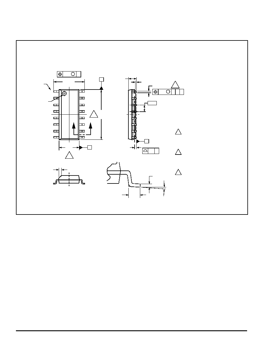
PACKAGE DIMENSIONS
NOTES:
1.
DIMENSIONS ARE IN MILLIMETERS.
2.
DIMENSIONING AND TOLERANCING PER ASME
Y14.5M, 1994.
3.
DATUMS A AND B TO BE DETERMINED AT THE PLANE
WHERE THE BOTTOM OF THE LEADS EXIT THE
PLASTIC BODY.
4.
THIS DIMENSION DOES NOT INCLUDE MOLD FLASH,
PROTRUSION OR GATE BURRS. MOLD FLASH,
PROTRUSION OR GATE BURRS SHALL NOT EXCEED
0.15 MM PER SIDE. THIS DIMENSION IS DETERMINED
AT THE PLANE WHERE THE BOTTOM OF THE LEADS
EXIT THE PLASTIC BODY.
5.
THIS DIMENSION DOES NOT INCLUDE INTER-LEAD
FLASH OR PROTRUSIONS. INTER-LEAD FLASH AND
PROTRUSIONS SHALL NOT EXCEED 0.25 MM PER
SIDE. THIS DIMENSION IS DETERMINED AT THE
PLANE WHERE THE BOTTOM OF THE LEADS EXIT
THE PLASTIC BODY.
6.
THIS DIMENSION DOES NOT INCLUDE DAMBAR
PROTRUSION. ALLOWABLE DAMBAR PROTRUSION
SHALL NOT CAUSE THE LEAD WIDTH TO EXCEED
0.62 MM.
8
9
1
16
SEATING
PLANE
7
0.50
X45
∞
8X
M
0.25
B
0.49
16X
B
M
0.25
A
T
4
6.2
5.8
10.0
9.8
A
4.0
3.8
B
PIN 1 INDEX
PIN'S
NUMBER
5
A
A
0.25
1.25
0.40
0
0.25
0.19
∞
∞
SECTION A-A
0.35
1.75
1.35
0.25
0.10
6
T
16X
0.1 T
1.27
14X
D SUFFIX
16-LEAD SOIC NARROW BODY
PLASTIC PACKAGE
CASE 751B-05
ISSUE K
F
r
e
e
s
c
a
l
e
S
e
m
i
c
o
n
d
u
c
t
o
r
,
I
Freescale Semiconductor, Inc.
For More Information On This Product,
Go to: www.freescale.com
n
c
.
.
.

MOTOROLA ANALOG INTEGRATED CIRCUIT DEVICE DATA
33793
23
NOTES
F
r
e
e
s
c
a
l
e
S
e
m
i
c
o
n
d
u
c
t
o
r
,
I
Freescale Semiconductor, Inc.
For More Information On This Product,
Go to: www.freescale.com
n
c
.
.
.

Information in this document is provided solely to enable system and software implementers to use Motorola products. There are no express or implied
copyright licenses granted hereunder to design or fabricate any integrated circuits or integrated circuits based on the information in this document.
Motorola reserves the right to make changes without further notice to any products herein. Motorola makes no warranty, representation or guarantee
regarding the suitability of its products for any particular purpose, nor does Motorola assume any liability arising out of the application or use of any product
or circuit, and specifically disclaims any and all liability, including without limitation consequential or incidental damages. "Typical" parameters which may be
provided in Motorola data sheets and/or specifications can and do vary in different applications and actual performance may vary over time. All operating
parameters, including "Typicals" must be validated for each customer application by customer's technical experts. Motorola does not convey any license
under its patent rights nor the rights of others. Motorola products are not designed, intended, or authorized for use as components in systems intended for
surgical implant into the body, or other applications intended to support or sustain life, or for any other application in which the failure of the Motorola product
could create a situation where personal injury or death may occur. Should Buyer purchase or use Motorola products for any such unintended or
unauthorized application, Buyer shall indemnify and hold Motorola and its officers, employees, subsidiaries, affiliates, and distributors harmless against all
claims, costs, damages, and expenses, and reasonable attorney fees arising out of, directly or indirectly, any claim of personal injury or death associated
with such unintended or unauthorized use, even if such claim alleges that Motorola was negligent regarding the design or manufacture of the part.
MOTOROLA and the Stylized M Logo are registered in the US Patent and Trademark Office. All other product or service names are the property of their
respective owners.
© Motorola, Inc. 2003
HOW TO REACH US:
USA/EUROPE/LOCATIONS NOT LISTED:
JAPAN: Motorola Japan Ltd.; SPS, Technical Information Center
Motorola Literature Distribution
3-20-1 Minami-Azabu. Minato-ku, Tokyo 106-8573, Japan
P.O. Box 5405, Denver, Colorado 80217
81-3-3440-3569
1-800-521-6274 or 480-768-2130
ASIA/PACIFIC: Motorola Semiconductors H.K. Ltd.; Silicon Harbour Centre
2 Dai King Street, Tai Po Industrial Estate, Tai Po, N.T., Hong Kong
852-26668334
HOME PAGE: http://motorola.com/semiconductors
MC33793/D
F
r
e
e
s
c
a
l
e
S
e
m
i
c
o
n
d
u
c
t
o
r
,
I
Freescale Semiconductor, Inc.
For More Information On This Product,
Go to: www.freescale.com
n
c
.
.
.