 | –≠–ª–µ–∫—Ç—Ä–æ–Ω–Ω—ã–π –∫–æ–º–ø–æ–Ω–µ–Ω—Ç: MC33998 | –°–∫–∞—á–∞—Ç—å:  PDF PDF  ZIP ZIP |
Document Outline
- Introduction
- 33998 Simplified Application Diagram
- 33998 Simplified Block Diagram
- Pin Function Description
- Maximum Ratings
- Static Electrical Characteristics
- Dynamic Electrical Characteristics
- Timing Diagrams
- System/Application Information
- Introduction
- Functional Pin Description
- Applications
- Package Dimensions

MOTOROLA
SEMICONDUCTOR TECHNICAL DATA
This document contains certain information on a new product.
Specifications and information herein are subject to change without notice.
© Motorola, Inc. 2003
33998 Simplified Application Diagram
Document order number: MC33998/D
Rev 1.0, 03/2003
33998
Advance Information
Switching Power Supply with Linear
Regulators
The 33998 is a medium-power, multi-output power supply integrated circuit
that is capable of operating over a wide input voltage range, from 6.0 V up to
26.5 V with 40 V transient capability. It incorporates a sensorless current
mode control step-down switching controller regulating directly to 5.0 V. The
2.6 V linear regulator uses an external pass transistor to reduce the 33998
power dissipation. The 33998 also provides a 2.6 V linear standby regulator
and two 5.0 V sensor supply outputs protected by internal low-resistance
LDMOS transistors.
There are two separate enable pins for the main and sensor supply outputs
and standard supervisory functions such as resets with power-up reset delay.
The 33998 provides proper power supply sequencing for advanced
microprocessor architectures such as the Motorola MPC5xx and 683xx
microprocessor families.
Features
∑ Operating Voltage Range 6.0 V up to 26.5 V (40 V transient)
∑ Step-Down Switching Regulator Output V
DDH
= 5.0 V @ 1400 mA (total)
∑ Linear Regulator with External Pass Transistor V
DDL
= 2.6 V @ 400 mA
∑ Low-Power Standby Linear Regulator V
KAM
= 2.6 V @ 10 mA
∑ Two 5.0 V @ 200 mA (typical) Sensor Supplies V
REF
Protected Against
Short-to-Battery and Short-to-Ground with Retry Capability
∑ Undervoltage Shutdown on the V
DDL
, V
DDH
Outputs with Retry Capability
∑ Reset Signals
∑ Power-Up Delay
∑ Enable Pins for Main Supplies (EN) and Sensor Supplies (SNSEN)
∑ Power Sequencing for Advanced Microprocessor Architectures
∑ SOIC-24WB Package
SNSEN
VREF1
5.0 V
VPWR
KA_VPWR
GND
33998
EN
VSW
VDDH
DRVL
FBL
PWROK
VKAM
VKAMOK
VREF2
5.0 V
5.0 V
2.6 V
2.6 V
MCU
VDDH
VDDL
VKAM
ORDERING INFORMATION
Device
Temperature
Range (T
A
)
Package
MC33998DW/R2
-40∞C to 125∞C
24 SOICW
DW SUFFIX
24-LEAD SOICW
CASE 751E
POWER SUPPLY
INTEGRATED CIRCUIT

33998
MOTOROLA ANALOG INTEGRATED CIRCUIT DEVICE DATA
2
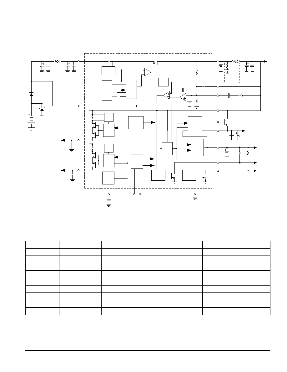
Figure 1. 33998 Simplified Block Diagram
SNSEN
VPW R
KA_VPW R
PGND
339 98
EN
VSW
VDDH
DRVL
FBL
PWROK
V KAM
VKAMOK
V bg
VRE F1
VRE F2
I -lim
Ramp
O sc
S oft
Start
Logic
&
Latch
PwrOK
VkamOK
POR
2.6V
Lin ear
Re gulat or
Driver
2. 6V
Standby
Reg.
B andgap
Voltage
Reference
Charge
Pump
VREF1
Reg.
VREF2
Reg.
Vbg
Vbg
CRES
VSUM
FBKB
En able
Co ntrol
E nb
Sn senb
5.0 V
5.0 V
2.6 V
5.0 V
2.6 V
Snsenb
S nsenb
Enb
Enb
Enb
Retry
Retry
Drive
MOTOROLA ANALOG INTEGRATED CIRCUIT DEVICE DATA
33998
3
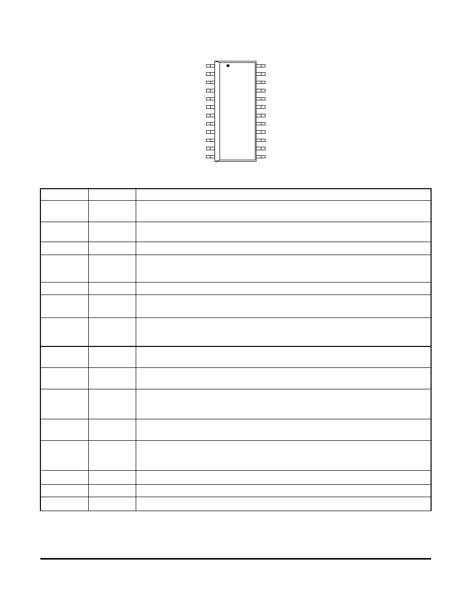
PIN FUNCTION DESCRIPTION
Pin
Pin Name
Description
1
VKAMOK
Keep-Alive Output Monitoring. This pin is an "open-drain" output that will be used with a discrete pull-up resistor
to V
KAM
. When the supply voltage to the 33998 is disconnected or lost, the VKAMOK signal goes low.
2
KA_V
PWR
Keep Alive Power Supply Pin. This supply pin is used in modules that have both direct battery connections and
ignition switch activated connections.
3
C
RES
Reservoir Capacitor. This pin is tied to an external "reservoir capacitor" for the internal charge pump.
4
V
PWR
Power Supply Pin. Main power input to the IC. This pin is directly connected to the switching regulator power
MOSFET. In automotive applications this pin must be protected against reverse battery conditions by an
external diode.
5≠8
GND
Ground of the integrated circuit.
9
V
SW
Internal P-Channel Power MOSFET Drain. V
SW
is the "switching node" of the voltage buck converter. This pin
is connected to the V
PWR
pin by an integrated p-channel MOSFET.
10
PWROK
Power OK Reset Pin. This pin is an "open-drain" output that will be used with a discrete pull-up resistor to
V
KAM
, V
DDH
, or V
DDL
. When either V
DDH
or V
DDL
output voltage goes out of the regulation limits this pin is
pulled down.
11
FBKB
Step-Down Switching Regulator Feedback Pin. The FBKB pin is the V
DDH
feedback signal for the switching
regulator.
12
V
SUM
Error Amplifier "Summing Node". The V
SUM
pin is connected to the inverting input of the error amplifier. This
node is also the "common" point of the integrated feedback resistor divider.
13
DRVL
Drive for V
DDL
(2.6 V) Regulator. The DRVL pin drives the base of an external NPN pass transistor for the
V
DDL
linear post regulator. The collector of the VDDL pass transistor is connected to V
DDH
. An example of a
suitable pass transistor is BCP68.
14
FBL
Feedback for V
DDL
(2.6 V) Regulator. The FBL pin is the voltage feedback sense signal from the V
DDL
(2.6 V)
linear post regulator.
15
V
DDH
V
DDH
is an input supply pin providing power for the buffered sensor supplies and the drive circuitry for the 2.6 V
linear power regulator. The V
DDH
pin is supplied from the switching regulator output, capable of providing 5.0 V
@ 1400 mA total output current.
16
V
REF2
Sensor Supply #2 Output. The V
REF2
pin is sensor supply output #2.
17≠20
GND
Ground of the integrated circuit.
21
V
REF1
Sensor Supply #1 Output. The V
REF1
pin is sensor supply output #1.
V
KAM
GND
GND
GND
GND
V
REF2
V
DDH
FBL
DRVL
EN
SNSEN
V
REF1
VKAMOK
GND
GND
GND
GND
V
SW
PWROK
V
SUM
KA_V
PWR
C
RES
V
PWR
FBKB
5
6
7
8
9
10
11
12
2
3
4
24
20
19
18
17
16
15
13
23
22
21
14
1
33998
MOTOROLA ANALOG INTEGRATED CIRCUIT DEVICE DATA
4
22
SNSEN
Sensor Supply Enable Input. The SNSEN pin is an input, which enables the V
REF1
and V
REF2
supplies. It
allows the control module hardware/software to shut down the sensor supplies.
23
EN
Enable Input. The EN pin is an input, which enables the main switching regulator and all other functions. When
this pin is low, the power supply is in a low quiescent state.
24
V
KAM
Keep-Alive (standby) 2.6 V Regulator Output. This is a 2.6 V low quiescent, low dropout regulator for Keep
Alive memory.
PIN FUNCTION DESCRIPTION (continued)
Pin
Pin Name
Description
MOTOROLA ANALOG INTEGRATED CIRCUIT DEVICE DATA
33998
5
MAXIMUM RATINGS
All voltages are with respect to ground unless otherwise noted.
Rating
Symbol
Value
Unit
Main Supply Voltage
V
PWR
-0.3 to 45
V
Keep-Alive Supply Voltage
KA_V
PWR
-0.3 to 45
V
Switching Node
V
SW
-0.5 to 45
V
5.0 V Input Power
V
DDH
-0.3 to 6.0
V
Sensor Supply
V
REF1
V
REF2
-0.3 to 18
-0.3 to 18
V
Keep-Alive Supply Voltage
V
KAM
-0.3 to 6.0
V
Maximum Voltage at Logic I/O Pins
EN
SNSEN
PWROK
VKAMOK
-0.3 to 6.0
-0.3 to 6.0
-0.3 to 6.0
-0.3 to 6.0
V
Charge Pump Reservoir Capacitor Voltage
C
RES
-0.3 to 18
V
Error Amplifier Summing Node
V
SUM
-0.3 to 6.0
V
Switching Regulator Output Feedback
FBKB
-0.3 to 6.0
V
V
DDL
Base Drive
DRVL
-0.3 to 6.0
V
V
DDL
Feedback
FBL
-0.3 to 6.0
V
ESD Voltage
Human Body Model (all pins) (Note 1)
Machine Model (all pins) (Note 2)
V
ESD1
V
ESD2
±500
±100
V
Power Dissipation (T
A
= 25
∞C) (Note 3)
P
D
800
mW
Thermal Resistance, Junction to Ambient (Note 4), (Note 5)
R
J-A
60
∞C/W
Thermal Resistance, Junction to Board (Note 6)
R
J-B
20
∞C/W
Operational Package Temperature [Ambient Temperature] (Note 7)
T
A
-40 to 125
∞C
Operational Junction Temperature
T
J
-40 to 150
∞C
Storage Temperature
T
STG
-55 to 150
∞C
Lead Soldering Temperature (Note 8)
T
S
260
∞C
Notes
1.
ESD1 testing is performed in accordance with the Human Body Model (C
ZAP
=100 pF, R
ZAP
=1500
).
2.
ESD2 testing is performed in accordance with the Machine Model (C
ZAP
=200 pF, R
ZAP
=0
)
3.
Maximum power dissipation at indicated junction temperature.
4.
Junction temperature is a function of on-chip power dissipation, package thermal resistance, mounting site (board) temperature, ambient
temperature, air flow, power dissipation of other components on the board, and board thermal resistance.
5.
Per SEMI G38-87 and JEDEC JESD51-2 with the single layer board horizontal.
6.
Thermal resistance between the die and the printed circuit board per JEDEC JESD51-8. Board temperature is measured on the top surface
of the board near the package.
7.
The limiting factor is junction temperature, taking into account the power dissipation, thermal resistance, and heat sinking.
8.
Lead soldering temperature limit is for 10 seconds maximum duration. Not designed for immersion soldering. Exceeding these limits may
cause malfunction or permanent damage to the device.

33998
MOTOROLA ANALOG INTEGRATED CIRCUIT DEVICE DATA
6
STATIC ELECTRICAL CHARACTERISTICS
Characteristics noted under conditions 9.0 V
V
PWR
16 V, -40
∞C
T
J
= T
A
125
∞C, using the typical application circuit (see
Figure 8
) unless otherwise noted. Typical values noted reflect the approximate parameter mean at T
A
= 25
∞C under nominal
conditions unless otherwise noted.
Characteristic
Symbol
Min
Typ
Max
Unit
GENERAL
Supply Voltage Range
Normal Operating Voltage Range (Note 9)
Extended Operating Voltage Range (Note 9)
V
PWR(N)
V
PWR(E)
6.0
18
≠
≠
18
26.5
V
Maximum Transient Voltage - Load Dump (Note 10)
V
PWR(LD)
≠
≠
40
V
V
PWR
Supply Current
EN = 5.0 V, V
PWR
= 14 V, No Loads
I
VPWR
25
≠
150
mA
V
PWR
Quiescent Supply Current
EN = 0 V, V
PWR
= 12 V
I
Q_VPWR
5.0
≠
15
µA
KA_V
PWR
Supply Current,
EN = 5.0 V, KA_V
PWR
= 14 V, No Load on V
KAM
I
KAVPWR
0.5
≠
3.0
mA
KA_V
PWR
Quiescent Supply Current
EN = 0 V, KA_V
PWR
= 12 V
I
Q_KAVPWR
50
≠
350
µA
BUCK REGULATOR V
DDH
Buck Converter Output Voltage
I
VDDH
= 200 mA to 1.4 A, V
PWR
= KA_V
PWR
= 14 V
V
DDH
4.9
≠
5.1
V
Buck Converter Output Voltage
I
VDDH
= 1.4 A, V
PWR
= KA_V
PWR
= 6.0 V
V
DDH
4.9
≠
5.1
V
V
DDH
Line Regulation
V
PWR
= KA_V
PWR
= 10 V to 14 V, I
VDDH
= 200 mA
RegLn
VDDH
-20
≠
30
mV
V
DDH
Load Regulation
V
PWR
= KA_V
PWR
= 14 V, I
VDDH
= 200 mA to 1.4 A
V
PWR
= KA_V
PWR
= 6.0 V, I
VDDH
= 200 mA to 1.4 A
RegLd
VDDH
-20
-20
≠
≠
20
20
mV
V
DDH
Active Discharge Resistance
V
PWR
= KA_V
PWR
= 14 V, EN = 0 V, I
VDDH
= 10 mA
R
HDisch
1.0
≠
15
P-CHANNEL MOSFET
Drain-Source Breakdown Voltage--Not Tested (Note 11)
BV
DSS
45
≠
≠
V
Drain-Source Current Limit--Not Tested (Note 11)
Isc
SW1
≠
-7.0
≠
A
Notes
9.
V
DDH
is fully functional when the 33998 is operating at higher battery voltages, but these parameters are not tested. The test condition as are:
a) V
DDH
must be between 4.9 V and 5.1 V (200 mA to 1.4 A) for V
PWR
= 14 V to 18 V.
b) V
DDH
must be between 4.8 V and 5.5 V (200 mA to 1.4 A) for V
PWR
= 18 V to 26.5 V.
10.
Part can survive, but no parameters are guaranteed.
11.
Guaranteed by design but not production tested.

MOTOROLA ANALOG INTEGRATED CIRCUIT DEVICE DATA
33998
7
STATIC ELECTRICAL CHARACTERISTICS (continued)
Characteristics noted under conditions 9.0 V
V
PWR
16 V, -40
∞C
T
J
= T
A
125
∞C, using the typical application circuit (see
Figure 8
) unless otherwise noted. Typical values noted reflect the approximate parameter mean at T
A
= 25
∞C under nominal
conditions unless otherwise noted.
Characteristic
Symbol
Min
Typ
Max
Unit
LINEAR REGULATOR V
DDL
V
DDL
Output Voltage
V
PWR
= KA_V
PWR
= 14 V, I
VDDL
= 200 mA
V
DDL
2.5
2.6
2.7
V
V
DDL
Line Regulation
V
DDH
= 4.8 V to 5.2 V, I
VDDL
= 400 mA
RegLn
VDDL
-30
≠
30
mV
V
DDL
Load Regulation
V
PWR
= KA_V
PWR
= 14 V, I
VDDL
= 10 mA to 400 mA
RegLd
VDDL
-70
≠
70
mV
DRVL Output Current
V
PWR
= KA_V
PWR
= 14 V, VDRVL = 1.0 V
I
DRVL
5.0
11
25
mA
V
DDL
Active Discharge Resistance
V
PWR
= KA_V
PWR
= 14 V, EN = 0 V, I
FBL
= 10 mA
R
LDisch
1.0
≠
10
V
DDH
to V
DDL
Active Clamp Resistance
V
PWR
= KA_V
PWR
= 14 V, EN = 0 V, I
VDDH
= 50 mA, V
FBKB
= 0 V
R
CLAMP
0.6
≠
10
V
DDL
Output Capacitor Capacitance (Note 12)
C
VDDL
≠
68
≠
µF
V
DDL
Output Capacitor ESR (Note 12)
ESR
VDDL
≠
0.125
≠
KEEP-ALIVE (STANDBY) REGULATOR V
KAM
V
KAM
Output Voltage
I
VKAM
= 5.0 mA, VPWR = KA_V
PWR
= 18 V, EN = 5.0 V
V
KAM
2.5
≠
2.7
V
V
KAM
Output Voltage, EN = 0 V (Standby Mode)
V
PWR
= KA_V
PWR
= 26 V, I
VKAM
= 0.5 mA
V
PWR
= KA_V
PWR
= 18 V, I
VKAM
= 5.0 mA
V
PWR
= KA_V
PWR
= 5.0 V, I
VKAM
= 10.0 mA
V
PWR
= 0 V, KA_V
PWR
= 3.5 V, I
VKAM
= 5.0 mA
V
KAM
2.5
2.5
2.5
2.0
≠
≠
≠
≠
2.7
2.7
2.7
2.7
V
V
KAM
Line Regulation, EN = 0 V (Standby Mode)
V
PWR
= KA_V
PWR
= 5.0 V to 18 V, I
VKAM
= 2.0 mA
RegLn
VKAM
-20
≠
20
mV
V
KAM
Load Regulation, EN = 0 V (Standby Mode)
V
PWR
= KA_V
PWR
= 14 V, I
VKAM
= 1.0 mA to 10 mA
RegLd
VKAM
0
≠
100
mV
Differential Voltage V
KAM
- V
DDL
EN = 5.0 V, I
VKAM
= 5.0 mA, V
PWR
= KA_V
PWR
= 14 V, I
VDDL
= 200 mA
Reg
VKAM
-20
≠
60
mV
V
KAM
Output Capacitor Capacitance (Note 12)
C
VKAM
≠
4.7
≠
µF
V
KAM
Output Capacitor ESR (Note 12)
ESR
VKAM
≠
1.4
≠
Notes
12.
Recommended value.

33998
MOTOROLA ANALOG INTEGRATED CIRCUIT DEVICE DATA
8
Characteristic
Symbol
Min
Typ
Max
Unit
SENSOR SUPPLIES V
REF1
, V
REF2
V
REF
On-Resistance, T
A
= -40∞C
I
VREF
= 200 mA, I
VDDH
= 200 mA, V
PWR
= KA_V
PWR
= 14 V, EN = 5.0 V
R
DS(on)
≠
≠
280
m
V
REF
On-Resistance, T
A
= +25∞C
I
VREF
= 200 mA, I
VDDH
= 200 mA, V
PWR
= KA_V
PWR
= 14 V, EN = 5.0 V
R
DS(on)
≠
≠
350
m
V
REF
On-Resistance, T
A
= +125∞C
I
VREF
= 200 mA, I
VDDH
= 200 mA, V
PWR
= KA_V
PWR
= 14 V, EN = 5.0 V
R
DS(on)
≠
≠
455
m
V
REF
Short-to-Battery Detect Current
V
PWR
= KA_V
PWR
= 14 V, EN = 5.0 V, SNSEN = 5.0 V
I
SC_Bat
500
≠
900
mA
V
REF
Short-to-Ground Detect Current
V
PWR
= KA_V
PWR
= 14 V, EN = 5.0 V, SNSEN = 5.0 V
I
SC_Gnd
500
≠
900
mA
Maximum Output Capacitance (Total) (Note 13)
C
VREF
33
≠
39
nF
SUPERVISORY CIRCUITS
PWROK Undervoltage Threshold on V
DDL
, FBL Ramps Down
V
PWR
= KA_V
PWR
= 14 V, I
VDDH
= 200 mA
V
FBL(thL)
2.1
2.4
2.5
V
PWROK Undervoltage Threshold on V
DDH
V
PWR
= KA_V
PWR
= 14 V, I
VDDH
= 200 mA
V
DDH(thL)
4.5
≠
4.8
V
V
DDH
Overvoltage Threshold
V
PWR
= KA_V
PWR
= 10 V, I
VDDH
= 200 mA
V
DDH(thH)
5.12
≠
5.7
V
PWROK Open Drain On-Resistance
V
PWR
= KA_V
PWR
= 14 V, EN = 5 V, I
PwrOK
= 5.0 mA
R
DS(on)
≠
≠
200
VKAMOK Threshold,
V
PWR
= KA_V
PWR
= 14 V, I
VDDH
= 200 mA
V
KAM(thL)
2.1
2.4
2.5
V
VKAMOK Threshold on V
PWR
, V
PWR
Ramps Up
KA_V
PWR
= 14 V, I
VDDH
= 200 mA
V
PWRok(th)
4.0
≠
5.0
V
VKAMOK Open Drain On-Resistance
V
PWR
= KA_V
PWR
= 14 V, EN = 0 V, I
VKAMOK
= 10 mA
R
DS(on)
50
≠
200
Enable Input Voltage Threshold (Pin EN)
V
IH
1.0
≠
2.0
V
Enable Pull-Down Current (Pin EN), EN = 1.0 V V
DDH
to V
IL(min)
I
PD
500
≠
1200
nA
Sensor Enable Input Voltage Threshold (Pin SNSEN)
V
IH
1.0
≠
2.0
V
Sensor Enable Pull-Down Current (Pin SNSEN)
SNSEN = 1.0 V V
DDH
to V
IL(min)
I
PD
500
≠
1200
nA
Notes
13.
Recommended value.
STATIC ELECTRICAL CHARACTERISTICS (continued)
Characteristics noted under conditions 9.0 V
V
PWR
16 V, -40
∞C
T
J
= T
A
125
∞C, using the typical application circuit (see
Figure 8
) unless otherwise noted. Typical values noted reflect the approximate parameter mean at T
A
= 25
∞C under nominal
conditions unless otherwise noted.
MOTOROLA ANALOG INTEGRATED CIRCUIT DEVICE DATA
33998
9
Characteristic
Symbol
Min
Typ
Max
Unit
CHARGE PUMP C
RES
Charge Pump Voltage
V
PWR
= KA_V
PWR
= 14 V, I
VDDH
= 200 mA, I
CP
= 0
µA
V
PWR
= KA_V
PWR
= 14 V, I
VDDH
= 200 mA, I
CP
= 10
µA
V
CRES
12
12
≠
≠
15
15
V
STATIC ELECTRICAL CHARACTERISTICS (continued)
Characteristics noted under conditions 9.0 V
V
PWR
16 V, -40
∞C
T
J
= T
A
125
∞C, using the typical application circuit (see
Figure 8
) unless otherwise noted. Typical values noted reflect the approximate parameter mean at T
A
= 25
∞C under nominal
conditions unless otherwise noted.

33998
MOTOROLA ANALOG INTEGRATED CIRCUIT DEVICE DATA
10
DYNAMIC ELECTRICAL CHARACTERISTICS
Characteristics noted under conditions 9.0 V
V
PWR
16 V, -40
∞C
T
J
= T
A
125
∞C using the typical application circuit (see
Figure 8
) unless otherwise noted. Typical values noted reflect the approximate parameter mean at T
A
= 25
∞C under nominal
conditions unless otherwise noted.
Characteristic
Symbol
Min
Typ
Max
Unit
BUCK REGULATOR V
DDH
Switching Frequency (Note 14)
f
SW
≠
750
≠
kHz
Soft Start Duration (see
Figure 2
)
V
PWR
= KA_V
PWR
= 6.0 V
t
SS
5.0
≠
15
ms
CHARGE PUMP C
RES
Charge Pump Current Ramp-Up Time
V
PWR
= KA_V
PWR
= 14 V, C
RES
= 22 nF, V
CP
= 1.0 V to 11 V
t
CRES
1.0
≠
20
ms
Charge Pump Ramp-Up Time
V
PWR
= KA_V
PWR
= 7.0 V, C
RES
= 22 nF, V
CP
= 7.0 V to 10 V
t
CRES
1.0
≠
10
ms
SENSOR SUPPLIES V
REF1
, V
REF2
V
REF
Overcurrent Detection Time (see
Figure 3
)
V
REF
Load R
L
= 5.0
to GND, V
DDH
= 5.1 V, V
PWR
= KA_V
PWR
= 10 V,
EN = 5.0 V, SNSEN = 5.0 V
t
Det
0.5
≠
2.0
µs
V
REF
Retry Timer Delay (see
Figure 3
)
V
REF
Load R
L
= 5.0
to GND, V
DDH
= 5.1 V, V
PWR
= KA_V
PWR
= 10 V,
EN = 5.0 V, SNSEN = 5.0 V
t
Ret
5.0
≠
20
ms
SUPERVISORY CIRCUITS
PWROK Delay Time (Power-On Reset) (see
Figure 4
)
t
D(PWROK)
5.0
≠
15
ms
VKAMOK Delay Time (see
Figure 5
)
t
D(VKAMOK)
10
≠
30
ms
V
DDH
Power-Up Delay Time (see
Figure 6
)
t
D(VPWR)
1.0
≠
10
ms
Fault-Off Timer Delay Time (see
Figure 7
)
t
Fault
1.0
≠
10
ms
Notes
14.
Guaranteed by design but not production tested.

MOTOROLA ANALOG INTEGRATED CIRCUIT DEVICE DATA
33998
11
Timing Diagrams
Figure 2. Soft-Start Time
Figure 3. V
REF
Retry Timer
Figure 4. PWROK Delay Timer (Power-On Reset)
4.8V
tSS
0
5.0
0
0
6.0
K
A
_
V
P
W
R
V
D
D
H
(
V
)
E
N
(
V
)
5.0
V
P
W
R
(
V
)
TIME
(
V
)
2.5V
0
5.0
0
0
14
K
A
_
V
P
W
R
V
R
E
F
(
V
)
E
N
(
V
)
5.0
V
P
W
R
(
V
)
0
2.6
P
W
R
O
K
(
V
)
??V
TIME
2.0V
tRet
??V
S
N
S
E
N
tDet
4.8V
2.0V
0
5.0
0
0
14
K
A
_
V
P
W
R
V
D
D
H
(
V
)
E
N
(
V
)
5.0
V
P
W
R
(
V
)
(
V
)
tD(PWROK)
0
2.6
P
W
R
O
K
(
V
)
4.6V
TIME

33998
MOTOROLA ANALOG INTEGRATED CIRCUIT DEVICE DATA
12
Timing Diagrams (continued)
Figure 5. VKAMOK Delay Time
Figure 6. V
DDH
Power-Up Delay Time
Figure 7. Fault-Off Timer Delay Time
tD(VKAMOK)
0
5.0
0
0
0
6.0
K
A
_
V
P
W
R
(
V
)
VPWR = 0V
V
K
A
M
O
K
(
V
)
V
K
A
M
(
V
)
2.6
E
N
(
V
)
TIME
2.4V
2.6
2.0V
tD(VPWR)
0
5.0
0
0
0
18
K
A
_
V
P
W
R
V
D
D
H
(
V
)
V
P
W
R
(
V
)
18
E
N
(
V
)
5.0
(
V
)
TIME
0
5.0
0
0
14
K
A
_
V
P
W
R
V
D
D
H
(
V
)
E
N
(
V
)
5.0
V
P
W
R
(
V
)
tFault
0
2.6
P
W
R
O
K
(
V
)
4.7V
0
2.6
V
D
D
L
TIME
1.0V
tFault
4.7V
1.0V
(
V
)

MOTOROLA ANALOG INTEGRATED CIRCUIT DEVICE DATA
33998
13
SYSTEM/APPLICATION INFORMATION
INTRODUCTION
The 33998 multi-output power supply integrated circuit is
capable of operating from 6.0 V up to 26.5 V with 40 V transient
capability. It incorporates a step-down switching controller
regulating directly to 5.0 V. The 2.6 V linear regulator uses an
external pass transistor, thus reducing the power dissipation of
the integrated circuit. The 33998 also provides a 2.6 V linear
standby regulator and two 5.0 V sensor supply outputs
protected by internal low-resistance LDMOS transistors
against short-to-battery and short-to-ground.
FUNCTIONAL PIN DESCRIPTION
Switching Regulator V
DDH
The switching regulator is a high-frequency (750 kHz),
conventional buck converter with integrated high-side p-
channel power MOSFET. Its output voltage is regulated to
provide 5.0 V with ±2% accuracy and it is intended to directly
power the digital and analog circuits of the Electronic Control
Module (ECM). The switching regulator output is rated for
1400 mA total output current. This current can be used by the
linear regulator V
DDL
and sensor supplies V
REF1
and V
REF2
.
The 33998 switching controller utilizes "Sensorless Current
Mode Control" to achieve good line rejection and stabilize the
feedback loop. A soft-start feature is incorporated into the
33998. When the device is enabled, the switching regulator
output voltage V
DDH
ramps up to about half of full scale and
then takes 16 steps up to the nominal regulation voltage level
(5.0 V nominal).
2.6 V Linear Regulator V
DDL
The 2.6 V linear post-regulator is powered from the 5.0 V
switching regulator output (V
DDH
). A discrete pass transistor is
used to the power path for the V
DDL
regulator. This
arrangement minimizes the power dissipation off the controller
IC. The FBL pin is the feedback input of the regulator control
loop and the DRVL pin the external NPN pass transistor base
drive. Power up, power down, and fault management are
coordinated with the 5.0 V switching regulator.
Sensor Supplies V
REF1
and V
REF2
The sensor supplies are implemented using a protected
switch to the main 5.0 V (switching regulator) output. The
33998 integrated circuit provides two low-resistance LDMOS
power MOSFETs connected to the switching regulator output
(V
DDH
). These switches have short-to-battery and short-to-
ground protection integrated into the IC. When a severe fault
conditions is detected, the affected sensor output is turned off
and the sensor Retry Timer starts to time out. After the Retry
Timer expires, the sensor supply tries to power up again.
Sensor supplies V
REF
can be disabled by pulling the Sensor
Enable SNSEN pin low (see
Figure 7
for the V
REF
Retry Timer
operation).
Notes: Severe fault conditions on the V
REF1
and V
REF2
outputs, like hard shorts to either ground or battery, may disrupt
the operation of the main regulator V
DDH
. Shorts to battery
above 17 V are considered "double faults" and neither one of
the V
REF
outputs is protected against such conditions.
Depending on the V
DDH
capacitor value and its ESR value,
the severity of the short may disrupt the V
DDH
operation.
Keep-Alive (Standby) Regulator V
KAM
The Keep-Alive Regulator V
KAM
(keep-alive memory) is
intended to provide power for "key off" functions such as
nonvolatile SRAM, "KeyOff" timers and controls, KeySwitch
monitor circuits, and perhaps a CAN/SCP monitor and wake-
up function. It may also power other low-current circuits
required during a "KeyOff" condition. The regulated voltage is
nominally 2.6 V. A severe fault condition on the V
KAM
output is
signaled by pulling the VKAMOK signal low.
V
KAM
Keep-Alive Operation (Standby, Power-Down
Mode)
When the EN pin is pulled low, the power supply is forced
into a low-current standby mode. In order to reduce current
drawn by the V
PWR
and KA_V
PWR
pins, all power supply
functions are disabled except for the V
KAM
and Enable (EN)
pins. The latter pin is monitored for the "wake-up" signal. The
switching transistor gate is actively disabled and the V
DDL
and
V
DDH
pins are actively pulled low.
Power-Up Delay Timers
Two Power-Up Delay timers are integrated into the control
section of the integrated circuit. One timer monitors the input
voltage at the V
PWR
input pin (see
Figure 3
), and the other
monitors the input voltage at the KA_V
PWR
input pin
.
In both
cases, sufficient supply voltage must be present long enough
for the timers to "time out" before the switching regulator can be
enabled.
Fault-Off Timer
If the V
DDL
output voltage does not reach its valid range at
the end of soft-start period, or if the V
DDH
or V
DDL
output
voltage gets below its PWROK threshold level, the Fault-Off
Timer shuts the switching regulator off until the timer "times
out" and the switching regulator retries to power up again (see
Figure 7
for Fault-Off Timer operation details).

33998
MOTOROLA ANALOG INTEGRATED CIRCUIT DEVICE DATA
14
Power-On Reset Timer
This timer starts to time out at the end of the soft-start period
if the V
DDH
and V
DDL
outputs are in the valid regulation range.
If the timer "times out", then the open-drain PWROK signal is
released, indicating that "power is ON".
Supervisory Circuits PWROK and VKAMOK
The 33998 has two voltage monitoring open-drain outputs,
the PWROK and the VKAMOK pins. PWROK is "active high".
This output is pulled low when either of the regulator outputs
(V
DDH
or V
DDL
) are below their regulation windows. If both
regulator outputs are above their respective lower thresholds,
and the Power-On Reset Timer has expired, the output driver is
turned off and this pin is at high-impedance state (see
Figure 6
).
The VKAMOK signal indicates a severe fault condition on
the keep-alive regulator output V
KAM
. The V
KAM
output voltage
is compared to the internal bandgap reference voltage. When
the V
KAM
falls below the bandgap reference voltage level, the
VKAMOK signal is pulled low.
MOTOROLA ANALOG INTEGRATED CIRCUIT DEVICE DATA
33998
15
APPLICATIONS
Figure 8. 33998 Application Circuit Schematic Diagram
Table 1. Recommended Components
Designator
Value/Rating
Description/Part No.
Manufacturer (Note 16)
Cf1
10 µF/50 V
Aluminum Electrolytic/UUB1H100MNR
Nichicon
Cf2, C2
1.0 µF/50 V
Ceramic X7R/C1812C105K5RACTR
Kemet
C1
100 µF/50 V
Aluminum Electrolytic/UUH1V101MNR
Nichicon
C3 (Note 15)
68 µF/10 V
Tantalum/T494D686M010AS
Kemet
C6
68 µF/10 V
Tantalum/T494D686M010AS
Kemet
C7
4.7 µF/10 V
Tantalum/T494A475M010AS
Kemet
C4, C5
100 nF/16 V
Ceramic X7R
Any Manufacturer
C8 (Optional)
390 pF/50 V
Ceramic X7R
Any Manufacturer
C9
22 nF/25 V
Ceramic X7R
Any Manufacturer
Notes
15.
It is possible to use ceramic capacitors in the switcher output, e.g. C3 = 2 x 22 µF/6.3 V X7R ceramic. In this case the compensation resistor
has to be changed to Rc1 = 200
to stabilize the switching regulator operation.
16.
Motorola does not assume liability, endorse, or warrant components from external manufacturers that are referenced in circuit drawings or
tables. While Motorola offers component recommendations in this configuration, it is the customer's responsibility to validate their application.
Note The V
DDH
total output current is 1.4 A. This includes the current used by the linear regulator V
DDL
and buffered outputs V
REF1
and
V
REF2
.
SNSEN
VPW R
KA _V PWR
G ND
3 399 8
EN
VSW
VDDH
DRVL
FB L
PW ROK
VKAM
VKAMOK
Vbg
VREF1
VREF2
I-lim
Ramp
O sc
Soft
St art
Logic
&
Latch
PwrO K
VkamO K
P OR
2. 6V
Linear
Regulat or
Driver
2.6V
St and by
Reg .
Ba ndgap
Voltage
Referen ce
Ch arge
Pump
VREF1
Re g.
VREF2
Re g.
Vbg
Vbg
CRES
VSUM
FBKB
Enable
Control
En b
Snsenb
Snsenb
Snsenb
E nb
Enb
Enb
Retry
Retry
Drive
C9
22n F
Cs1
33 nF
Lf1
10uH
C2
1.0uF
100uF
C1
Cf 2
1.0uF
10 uF
Cf1
Cs2
33nF
C6
68uF
1 00n F
C5
C4
100nF
68uF
C3
L1
15uH
C7
4 .7 uF
R1
1 0k
R2
10k
Q 1
Rc1
3.6k
Cc1
2.2nF
D1
Dp1
Dp 2
9
11
12
15
13
14
24
1
10
5-8
17 -20
22
23
3
16
21
2
4
VDDL = 2.6V
@ 40 0mA
VKAM = 2.6V
@ 10mA
VDDH = 5.0V
@ 1400mA total
C8
390 pF
R3
2 .2 R
O pt io nal
Snubber
33998
MOTOROLA ANALOG INTEGRATED CIRCUIT DEVICE DATA
16
Cs1, Cs2
33 nF/25 V
Ceramic X7R
Any Manufacturer
Cc1
2.2 nF/16 V
Ceramic X7R
Any Manufacturer
R1, R2
10 k
Resistor 0805, 5%
Any Manufacturer
R3 (Optional)
2.2
Resistor 0805, 5%
Any Manufacturer
Rc1
3.6 k
Resistor 0805, 5%
Any Manufacturer
Lf1
10 µH
CDRH127-100M
or SLF10145-100M2R5
Sumida
TDK
L1
15 µH
CDRH127-150MC
or SLF10145-150M2R2
Sumida
TDK
Q1
1.0 A/20 V
Bipolar Transistor/BCP68T1
ON Semiconductor
D1
2.0 A/50 V
Schottky Diode/SS25
General Semiconductor
Dp1
3.0 A/200 V
Diode/MURS320
ON Semiconductor
Dp2
27 V
Transient Voltage Suppressor/SM5A27
General Semiconductor
Notes
17.
Motorola does not assume liability, endorse, or warrant components from external manufacturers that are referenced in circuit drawings or
tables. While Motorola offers component recommendations in this configuration, it is the customer's responsibility to validate their application.
Designator
Value/Rating
Description/Part No.
Manufacturer (Note 16)
(Note 17)
MOTOROLA ANALOG INTEGRATED CIRCUIT DEVICE DATA
33998
17
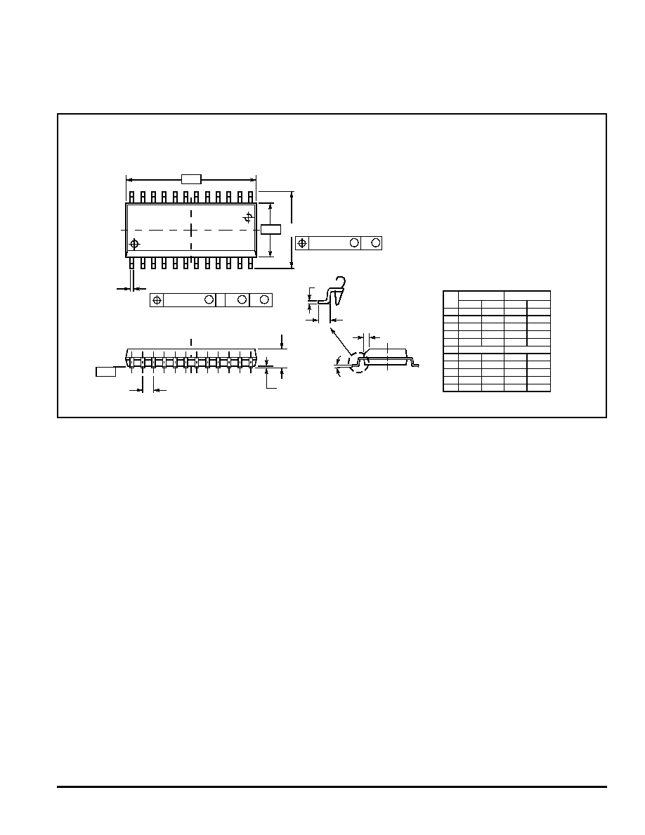
PACKAGE DIMENSIONS
NOTES:
1.
DIMENSIONING AND TOLERANCING PER ANSI
Y14.5M, 1982.
2.
CONTROLLING DIMENSION: MILLIMETER.
3.
DIMENSIONS A AND B DO NOT INCLUDE MOLD
PROTRUSION.
4.
MAXIMUM MOLD PROTRUSION 0.15 (0.006) PER
SIDE.
5.
DIMENSION D DOES NOT INCLUDE DAMBAR
PROTRUSION. ALLOWABLE DAMBAR
PROTRUSION SHALL BE 0.13 (0.005) TOTAL IN
EXCESS OF D DIMENSION AT MAXIMUM MATERIAL
CONDITION.
-A-
-B-
P
12X
D
24X
12
13
24
1
M
0.010 (0.25)
B
M
S
A
M
0.010 (0.25)
B
S
T
-T-
G
22X
SEATING
PLANE
K
C
R
X 45
∞
M
F
J
DIM
MIN
MAX
MIN
MAX
INCHES
MILLIMETERS
A
15.25
15.54
0.601
0.612
B
7.40
7.60
0.292
0.299
C
2.35
2.65
0.093
0.104
D
0.35
0.49
0.014
0.019
F
0.41
0.90
0.016
0.035
G
1.27 BSC
0.050 BSC
J
0.23
0.32
0.009
0.013
K
0.13
0.29
0.005
0.011
M
0
8
0
8
P
10.05
10.55
0.395
0.415
R
0.25
0.75
0.010
0.029
∞
∞
∞
∞
DW SUFFIX
24-LEAD SOIC WIDE BODY
PLASTIC PACKAGE
CASE 751E-04
ISSUE E

33998
MOTOROLA ANALOG INTEGRATED CIRCUIT DEVICE DATA
18
NOTES

MOTOROLA ANALOG INTEGRATED CIRCUIT DEVICE DATA
33998
19
NOTES

Information in this document is provided solely to enable system and software implementers to use Motorola products. There are no express or implied
copyright licenses granted hereunder to design or fabricate any integrated circuits or integrated circuits based on the information in this document.
Motorola reserves the right to make changes without further notice to any products herein. Motorola makes no warranty, representation or guarantee
regarding the suitability of its products for any particular purpose, nor does Motorola assume any liability arising out of the application or use of any product
or circuit, and specifically disclaims any and all liability, including without limitation consequential or incidental damages. "Typical" parameters which may be
provided in Motorola data sheets and/or specifications can and do vary in different applications and actual performance may vary over time. All operating
parameters, including "Typicals" must be validated for each customer application by customer's technical experts. Motorola does not convey any license
under its patent rights nor the rights of others. Motorola products are not designed, intended, or authorized for use as components in systems intended for
surgical implant into the body, or other applications intended to support or sustain life, or for any other application in which the failure of the Motorola product
could create a situation where personal injury or death may occur. Should Buyer purchase or use Motorola products for any such unintended or
unauthorized application, Buyer shall indemnify and hold Motorola and its officers, employees, subsidiaries, affiliates, and distributors harmless against all
claims, costs, damages, and expenses, and reasonable attorney fees arising out of, directly or indirectly, any claim of personal injury or death associated
with such unintended or unauthorized use, even if such claim alleges that Motorola was negligent regarding the design or manufacture of the part.
MOTOROLA and the Stylized M Logo are registered in the US Patent and Trademark Office. All other product or service names are the property of their
respective owners.
© Motorola, Inc. 2003
HOW TO REACH US:
USA/EUROPE/LOCATIONS NOT LISTED:
JAPAN: Motorola Japan Ltd.; SPS, Technical Information Center
Motorola Literature Distribution
3-20-1 Minami-Azabu. Minato-ku, Tokyo 106-8573, Japan
P.O. Box 5405, Denver, Colorado 80217
81-3-3440-3569
1-800-521-6274 or 480-768-2130
ASIA/PACIFIC: Motorola Semiconductors H.K. Ltd.; Silicon Harbour Centre
2 Dai King Street, Tai Po Industrial Estate, Tai Po, N.T., Hong Kong
852-26668334
HOME PAGE: http://motorola.com/semiconductors
MC33998/D