 | –≠–ª–µ–∫—Ç—Ä–æ–Ω–Ω—ã–π –∫–æ–º–ø–æ–Ω–µ–Ω—Ç: MC3403 | –°–∫–∞—á–∞—Ç—å:  PDF PDF  ZIP ZIP |
Device
Operating
Temperature Range
Package
MC3403
MC3303
SEMICONDUCTOR
TECHNICAL DATA
QUAD DIFFERENTIAL INPUT
OPERATIONAL AMPLIFIERS
ORDERING INFORMATION
MC3303D
MC3303P
MC3403D
MC3403P
TA = 0
∞
to +70
∞
C
TA = ≠ 40
∞
to +85
∞
C
SO≠14
Plastic DIP
SO≠14
Plastic DIP
PIN CONNECTIONS
Order this document by MC3403/D
D SUFFIX
PLASTIC PACKAGE
CASE 751A
(SO≠14)
P SUFFIX
PLASTIC PACKAGE
CASE 646
14
14
1
1
1
2
3
4
5
6
7
8
9
10
11
12
13
14
≠
+
≠
+
≠
+
≠
+
Out 1
Inputs 1
VCC
VEE/Gnd
Inputs 2
Out 2
Out 4
Inputs 4
Inputs 3
Out 3
1
2
3
4
(Top View)
1
MOTOROLA ANALOG IC DEVICE DATA
Quad Low Power
Operational Amplifiers
The MC3403 is a low cost, quad operational amplifier with true differential
inputs. The device has electrical characteristics similar to the popular
MC1741C. However, the MC3403 has several distinct advantages over
standard operational amplifier types in single supply applications. The quad
amplifier can operate at supply voltages as low as 3.0 V or as high as 36 V
with quiescent currents about one third of those associated with the
MC1741C (on a per amplifier basis). The common mode input range
includes the negative supply, thereby eliminating the necessity for external
biasing components in many applications. The output voltage range also
includes the negative power supply voltage.
∑
Short Circuit Protected Outputs
∑
Class AB Output Stage for Minimal Crossover Distortion
∑
True Differential Input Stage
∑
Single Supply Operation: 3.0 V to 36 V
∑
Split Supply Operation:
±
1.5 V to
±
18 V
∑
Low Input Bias Currents: 500 nA Max
∑
Four Amplifiers Per Package
∑
Internally Compensated
∑
Similar Performance to Popular MC1741C
∑
Industry Standard Pinouts
∑
ESD Diodes Added for Increased Ruggedness
3.0 V to 36 V
Single Supply
VEE, Gnd
1
2
3
4
VCC
VCC
2
3
4
VEE
1.5 V to 18 V
1.5 V to 18 V
Split Supplies
1
MAXIMUM RATINGS
Rating
Symbol
Value
Unit
Power Supply Voltages
Vdc
Single Supply
VCC
36
Split Supplies
VCC, VEE
±
18
Input Differential Voltage Range (Note 1)
VIDR
±
36
Vdc
Input Common Mode Voltage Range
(Notes 1, 2)
VICR
±
18
Vdc
Storage Temperature Range
Tstg
≠55 to +125
∞
C
Operating Ambient Temperature Range
TA
∞
C
MC3303
≠40 to +85
MC3403
0 to +70
Junction Temperature
TJ
150
∞
C
NOTES: 1. Split power supplies.
2. For supply voltages less than
±
18 V, the absolute maximum input voltage is equal
to the supply voltage.
©
Motorola, Inc. 1996
Rev 5
MC3403 MC3303
2
MOTOROLA ANALOG IC DEVICE DATA
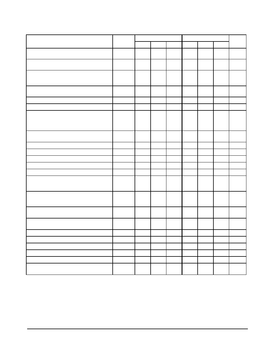
ELECTRICAL CHARACTERISTICS
(VCC = +15 V, VEE = ≠15 V for MC3403; VCC = +14 V, VEE = Gnd for MC3303
TA = 25
∞
C, unless otherwise noted.)
Ch
i i
S
b l
MC3403
MC3303
U i
Characteristic
Symbol
Min
Typ
Max
Min
Typ
Max
Unit
Input Offset Voltage
VIO
≠
2.0
10
≠
2.0
8.0
mV
TA = Thigh to Tlow (Note 1)
≠
≠
12
≠
≠
10
Input Offset Current
IIO
≠
30
50
≠
30
75
nA
TA = Thigh to Tlow
≠
≠
200
≠
≠
250
Large Signal Open Loop Voltage Gain
AVOL
V/mV
VO =
±
10 V, RL = 2.0 k
20
200
≠
20
200
≠
TA = Thigh to Tlow
15
≠
≠
15
≠
≠
Input Bias Current
IIB
≠
≠200
≠500
≠
≠200
≠500
nA
TA = Thigh to Tlow
≠
≠
≠800
≠
≠
≠1000
Output Impedance f = 20 Hz
zo
≠
75
≠
≠
75
≠
Input Impedance f = 20 Hz
zi
0.3
1.0
≠
0.3
1.0
≠
M
Output Voltage Range
VO
V
RL = 10 k
±
12
±
13.5
≠
12
12.5
≠
RL = 2.0 k
±
10
±
13
≠
10
12
≠
RL = 2.0 k
, TA = Thigh to Tlow
±
10
≠
≠
10
≠
≠
Input Common Mode Voltage Range
VICR
+13 V
≠VEE
+13 V
≠VEE
≠
+12 V
≠VEE
+12.5 V
≠VEE
≠
V
Common Mode Rejection RS
10 k
CMR
70
90
≠
70
90
≠
dB
Power Supply Current (VO = 0) RL =
ICC, IEE
≠
2.8
7.0
≠
2.8
7.0
mA
Individual Output Short≠Circuit Current (Note 2)
ISC
±
10
±
20
±
45
±
10
±
30
±
45
mA
Positive Power Supply Rejection Ratio
PSRR+
≠
30
150
≠
30
150
µ
V/V
Negative Power Supply Rejection Ratio
PSRR≠
≠
30
150
≠
30
150
µ
V/V
Average Temperature Coefficient of Input
Offset Current
TA = Thigh to Tlow
IIO/
T
≠
50
≠
≠
50
≠
pA/
∞
C
Average Temperature Coefficient of Input
Offset Voltage
TA = Thigh to Tlow
VIO/
T
≠
10
≠
≠
10
≠
µ
V/
∞
C
Power Bandwidth
AV = 1, RL = 10 k
,
VO = 20 V(p≠p), THD = 5%
BWp
≠
9.0
≠
≠
9.0
≠
kHz
Small≠Signal Bandwidth
AV = 1, RL = 10 k
,
VO = 50 mV
BW
≠
1.0
≠
≠
1.0
≠
MHz
Slew Rate AV = 1, Vi = ≠10 V to +10 V
SR
≠
0.6
≠
≠
0.6
≠
V/
µ
s
Rise Time AV = 1, RL = 10 k
,
VO = 50 mV
tTLH
≠
0.35
≠
≠
0.35
≠
µ
s
Fall Time AV = 1, RL = 10 k
,
VO = 50 mV
tTLH
≠
0.35
≠
≠
0.35
≠
µ
s
Overshoot AV = 1, RL = 10 k
,
VO = 50 mV
os
≠
20
≠
≠
20
≠
%
Phase Margin AV = 1, RL = 2.0 k
,
VO = 200 pF
m
≠
60
≠
≠
60
≠
Degrees
Crossover Distortion
(Vin = 30 mVpp,Vout= 2.0 Vpp, f = 10 kHz)
≠
≠
1.0
≠
≠
1.0
≠
%
NOTES: 1. Thigh = +70
∞
C for MC3403, +85
∞
C for MC3303
Tlow = 0
∞
C for MC3403, ≠40
∞
C for MC3303
2. Not to exceed maximum package power dissipation.

MC3403 MC3303
3
MOTOROLA ANALOG IC DEVICE DATA
ELECTRICAL CHARACTERISTICS
(VCC = 5.0 V, VEE = Gnd, TA = 25
∞
C, unless otherwise noted.)
Ch
i i
S
b l
MC3403
MC3303
U i
Characteristic
Symbol
Min
Typ
Max
Min
Typ
Max
Unit
Input Offset Voltage
VIO
≠
2.0
10
≠
≠
10
mV
Input Offset Current
IIO
≠
30
50
≠
≠
75
nA
Input Bias Current
IIB
≠
≠200
≠500
≠
≠
≠500
nA
Large Signal Open Loop Voltage Gain
RL = 2.0 k
AVOL
10
200
≠
10
200
≠
V/mV
Power Supply Rejection Ratio
PSRR
≠
≠
150
≠
≠
150
µ
V/V
Output Voltage Range (Note 3)
VOR
Vpp
RL = 10 k
, VCC = 5.0 V
3.3
3.5
≠
3.3
3.5
≠
RL = 10 k
, 5.0
VCC
30 V
VCC≠2.0 VCC≠1.7
≠
VCC≠2.0 VCC≠1.7
≠
Power Supply Current
ICC
≠
2.5
7.0
≠
2.5
7.0
mA
Channel Separation
f = 1.0 kHz to 20 kHz
(Input Referenced)
CS
≠
≠120
≠
≠
≠120
≠
dB
NOTES: 3. Output will swing to ground with a 10 k
pull down resistor.
Representative Schematic Diagram
(1/4 of Circuit Shown)
VEE (Gnd)
VCC
Output
Q23
Inputs
+
Q2
Q3
Q4
Q5
Q6
Q7
Q8
Q9
Q10
Q11
Q12
Q13
Q15
Q16
Q17
Q18
Q19
Q20
Q21
Q22
Q1
Q24
Q25
Q27
Q28
Q29
Q30
60 k
37 k
25
40 k
2.4 k
2.0 k
31k
5.0 pF
Bias Circuitry
Common to Four
Amplifiers
≠
MC3403 MC3303
4
MOTOROLA ANALOG IC DEVICE DATA
CIRCUIT DESCRIPTION
Inverter Pulse Response
20
µ
s/DIV
5.0 V/DIV
The MC3403/3303 is made using four internally
compensated, two≠stage operational amplifiers. The first
stage of each consists of differential input device Q24 and
Q22 with input buffer transistors Q25 and Q21 and the
differential to single ended converter Q3 and Q4. The first
stage performs not only the first stage gain function but also
performs the level shifting and transconductance reduction
functions. By reducing the transconductance, a smaller
compensation capacitor (only 5.0 pF) can be employed, thus
saving chip area. The transconductance reduction is
accomplished by splitting the collectors of Q24 and Q22.
Another feature of this input stage is that the input common
mode range can include the negative supply or ground, in
single supply operation, without saturating either the input
devices or the differential to single≠ended converter. The
second stage consists of a standard current source load
amplifier stage.
The output stage is unique because it allows the output to
swing to ground in single supply operation and yet does not
exhibit any crossover distortion in split supply operation. This
is possible because Class AB operation is utilized.
Each amplifier is biased from an internal voltage regulator
which has a low temperature coefficient, thus giving each
amplifier good temperature characteristics as well as
excellent power supply rejection.
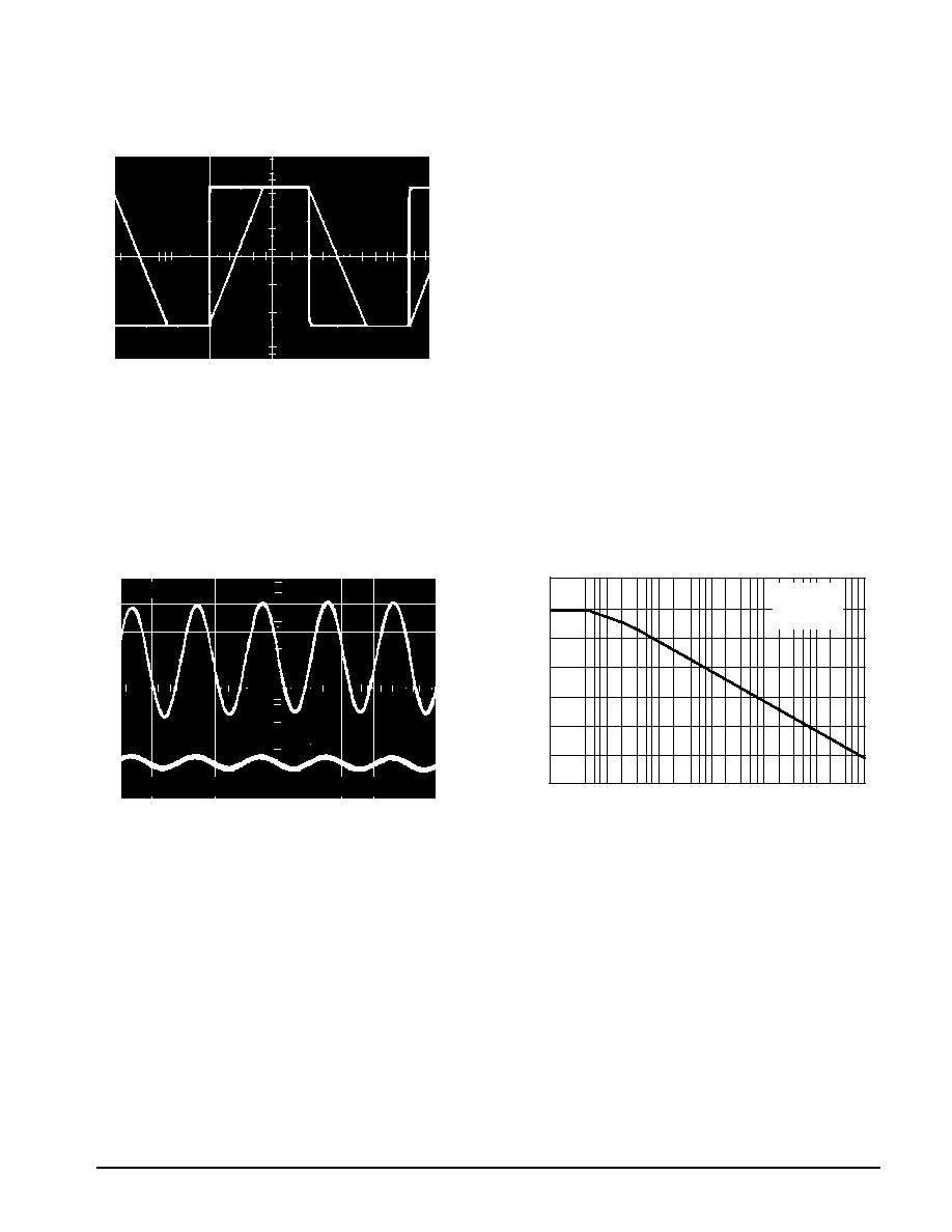
Figure 1. Sine Wave Response
Figure 2. Open Loop Frequency Response
A
OPEN LOOP
VOL
T
AGE GAIN (dB)
1.0
10
100
1.0 k
10 k
100 k
1.0 M
f, FREQUENCY (Hz)
≠20
0
20
40
60
80
100
120
, LARGE SIGNAL
VOL
50
µ
s/DIV
50 mV/DIV
0.5 V/DIV
AV = 100
*Note Class A B output stage produces distortion less sinewave.
VCC = 15 V
VEE = ≠15 V
TA = 25
∞
C
MC3403 MC3303
5
MOTOROLA ANALOG IC DEVICE DATA
V
O
,
OUTPUT
VOL
T
AGE (V
)
pp
1
2
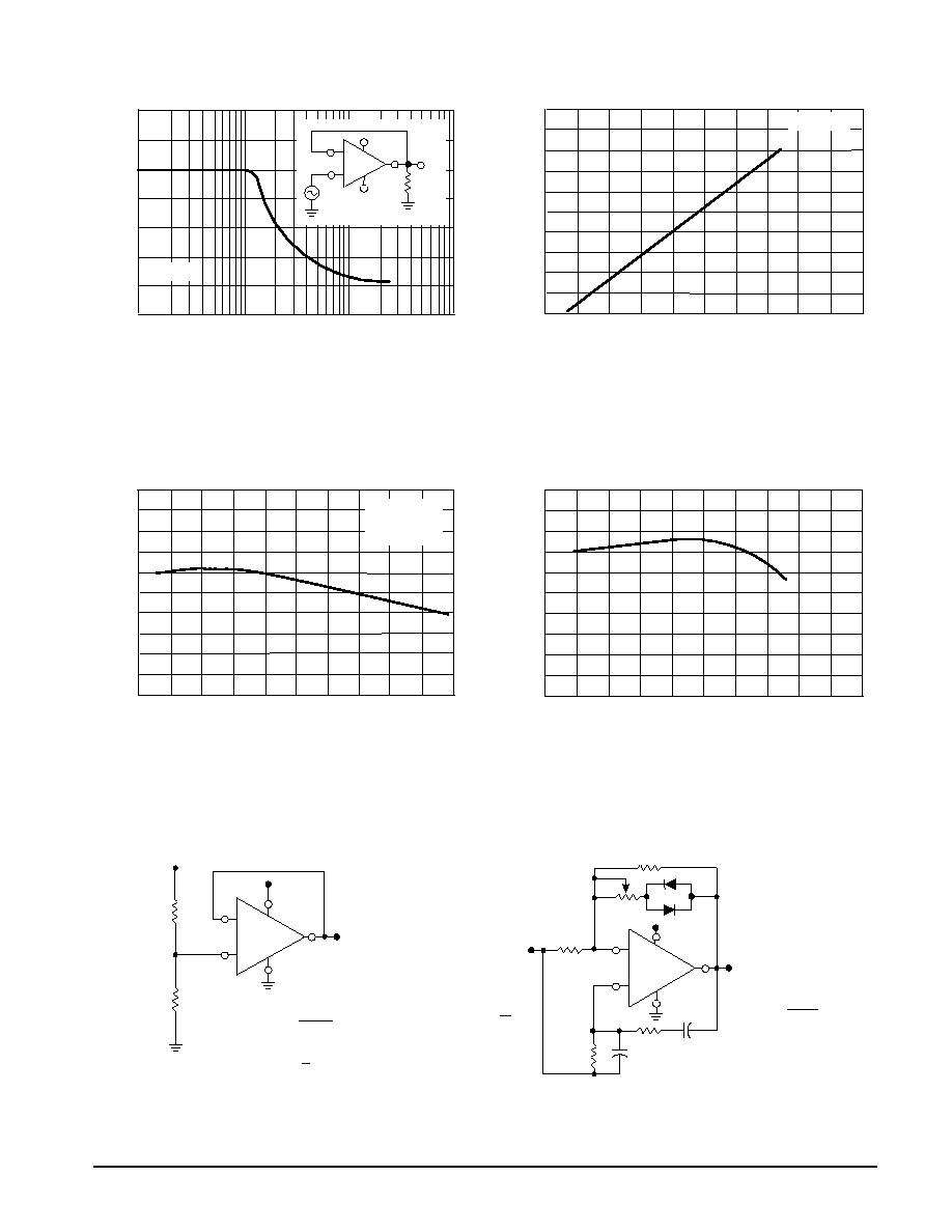
Figure 3. Power Bandwidth
Figure 4. Output Swing versus Supply Voltage
Figure 5. Input Bias Current
versus Temperature
Figure 6. Input Bias Current
versus Supply Voltage
f, FREQUENCY (Hz)
1.0 k
10 k
100 k
1.0 M
≠5.0
0
5.0
10
15
20
25
30
TA = 25
∞
C
O
+15 V
≠15 V
10 k
VO
≠
+
V O
0
2.0
4.0
6.0
8.0
10
12
14
16
18
20
VCC AND (VEE), POWER SUPPLY VOLTAGES (V)
0
20
30
10
TA = 25
∞
C
, OUTPUT
VOL
T
AGE RANGE (V pp)
T, TEMPERATURE (
∞
C)
≠75
≠55
≠35
≠15
5.0
25
45
65
85
105
125
100
200
300
, INPUT
BIAS CURRENT
(nA)
I IB
, INPUT
BIAS CURRENT
(nA)
I IB
VCC AND (VEE), POWER SUPPLY VOLTAGES (V)
0
2.0
4.0
6.0
8.0
10
12
14
16
18
20
150
160
170
Figure 7. Voltage Reference
Figure 8. Wien Bridge Oscillator
≠
+
VCC
10 k
R1
R2
VO
VCC
10 k
VO =
VO = VCC
R1
R1 +R2
1
2
1/2
MC3403
≠
+
10 k
VO
VCC
50 k
5.0 k
R
C
C
R
Vref = VCC
fo =
1
2
RC
fo = 1.0 kHz
R = 16 k
C = 0.01
µ
F
1/2
MC3403
Vref
VCC = 15 V
VEE = ≠15 V
TA = 25
∞
C
1N914
1N914
For: