 | –≠–ª–µ–∫—Ç—Ä–æ–Ω–Ω—ã–π –∫–æ–º–ø–æ–Ω–µ–Ω—Ç: MC68EZ328 | –°–∫–∞—á–∞—Ç—å:  PDF PDF  ZIP ZIP |
MC68EZ328P/D
Rev. 2
,
10/2001
This document contains information on a new product. Specifications and information
herein are subject to change without notice.
© Motorola, Inc., 2001. All rights reserved.
MC68EZ328
MC68EZ328 (DragonBallTM EZ)
Integrated Portable System Processor
Product Brief
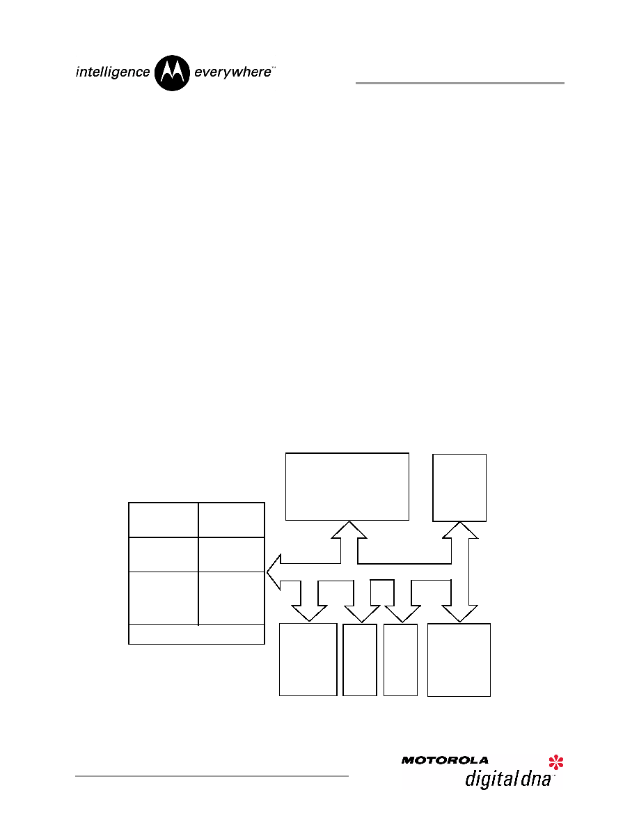
The second member of the DragonBall
family, the MC68EZ328 (shown in Figure 1), inherits the display capability of
the original DragonBall processor but features a more flexible LCD controller with a streamlined list of peripherals
placed in a smaller package. This processor is mainly targeted for portable consumer products which require less
peripherals and a more flexible LCD controller. By providing 3.3V, fully static operation in efficient 100 TQFP and
144 MAPBGA packages, the MC68EZ328
delivers cost-effective performance to satisfy the extensive
requirements of today's portable consumer market.
Figure 1. MC68EZ328 Block Diagram
16-BIT
TIMER
MODULE
68EC000 HCMOS
STATIC
CORE
UART
WITH
INFRA-RED
SUPPORT
SPI
LCD
CONTROLLER
RTC
SIZER AND
68EC000 INTERNAL BUS
8-/16-BIT
68000 BUS
INTERFACE
SYSTEM
PWM
PROCESSOR
CONTROL AND
INTEGRATION
INTERRUPT
CONTROLLER
MODULE (SIM28)
CLOCK SYNTHE-
DRAM CONTROLLER
EMULATION &
BOOTSTRAP
POWER CONTROL

2
MC68EZ328 Product Brief
1
Key Features
The primary features of the MC68EZ328 are as follows:
∑
Static 68EC000 Core Processor--Identical to MC68EC000 Microprocessor
--
Full compatibility with MC68000 and MC68EC000
--
32-Bit internal address bus
-- 24-Bit external address bus capable of addressing maximum 4 x 16MB blocks with chip selects CSA,
CSB and 4 x 4 MB blocks with chip selects CSC, CSD
--
16-Bit on-chip data bus for MC68000 bus operations
--
Static design allows processor clock to be stopped to provide power savings
--
2.7 MIPS Performance at 16.58 MHz processor clock and 3.25 MIPS Performance at 20 MHz processor
clock
--
External M68000 Bus interface with selectable bus sizing for 8-bit and 16-bit data ports
∑
System Integration Module (SIM28-EZ), incorporating many functions typically related to external array
logic, such as:
--
System configuration, programmable address mapping
--
Glueless interface to SRAM, EPROM, FLASH memory
--
8 programmable chip selects with wait state generation logic
--
4 programmable interrupt I/O and with keyboard interrupt capability
--
5 general purpose, programmable edge/level/polarity interrupt IRQ
--
Other programmable I/O, multiplexed with peripheral functions up to 47 parallel I/O
--
Programmable interrupt vector response for on-chip peripheral modules
--
Low-power mode control
∑
DRAM Controller
-- Support CAS-before-RAS refresh cycles and self-refresh mode DRAM
--
Support 8 bit / 16 bit port DRAM
--
EDO or Automatic Fast Page Mode for LCDC access
--
Programmable refresh rate
--
Support up to 2 banks of DRAM/EDO DRAM
--
Programmable column address size
∑
UART
--
Support IrDA physical layer protocol up to 115.2kbps
--
8 Bytes FIFO on Tx and 12 Bytes FIFO on Rx
∑
Serial Peripheral Interface Port
--
16 bit programmable SPI to support external peripherals
--
Master mode support
∑
16-Bit General Purpose Counter / Timer
--
Automatic interrupt generation
--
60-ns resolution at 16.58-MHz system clock

Key Features
3
--
Timer Input/Output pin
∑
Real Time Clock / Sampling Timer
--
Separate power supply for the RTC
--
One programmable alarm
--
Capable to count up to 512 days
--
Sampling Timer with selectable frequency (4Hz, 8Hz, 16Hz, 32Hz, 64Hz, 128Hz, 256Hz, 512Hz);
generate interrupt for digitizer sampling, or keyboard debouncing
∑
LCD Controller
-- Software programmable screen size (up to 640*512) to support single (Non-Split) monochrome
panels
-- Capable of direct driving popular LCD drivers/modules from Motorola, Sharp, Hitachi, Toshiba
etc.
-- Supports b/w, 4-grey and 16-grey level display
-- Utilize system memory as display memory
-- LCD contrast control using 8-bit PWM
∑
Pulse Width Modulation (PWM) Module
-- 8 bit resolution
-- 5 Byte FIFO provide more flexibility on performance
-- Sound and melody generation
∑
Built-in Emulation Function
-- Dedicated memory space for Emulator Debug Monitor with Chip Select
-- Dedicated interrupt (Interrupt Level 7) for ICE
-- One address signal comparator and one control signal comparator with masking to support
single or multiple Hardware Execution Breakpoint
-- One breakpoint instruction insertion unit
∑
Bootstrap Mode Function
-- Allows user to initialize system and download program/data to system memory through UART
-- Accept execution command to run program stored in system memory
-- Provide an 8-byte long Instruction Buffer for 68000 instruction storage and execution
∑
Power Management
-- Fully static HCMOS technology
-- Programmable clock synthesizer using 32.768 kHz/38.4 kHz crystal for full frequency control
-- Low power stop capabilities
-- Modules can be individually shut-down
-- Lowest power mode control
∑
Operation from DC To 16.58 MHz (processor clock)
∑
Operating voltage of (3.3 +/- 10%) V
∑
Compact 100-Lead and 144-Pin MAPBGA TQFP packages

4
MC68EZ328 Product Brief
System Configuration
2
System Integration Module
The MC68EZ328 system integration module (SIM28-EZ) consists of several functions that control the
system start-up, initialization, configuration, and the external bus with a minimum of external devices. The
memory interface allows the user to interface gluelessly with the widely available SRAM and EPROM as
well as FLASH memory. With the assistance of chip-select logic, wait states can be programmable. The
interrupt controller accepts and resolves the priority from internal modules and external generated
interrupts. It also handles the masking and wake-up selection control for power control. The low-power
logic can be used to control the CPU power dissipation by altering the frequency or stopping the CPU. In
addition, the SIM28-EZ is capable of configuring the pin to allow the user to select either dedicated I/O or
parallel I/O. This feature help to increase the number of available I/O ports by reclaiming when the
dedicated function is not used.
2.1
System Configuration
The MC68EZ328 system configuration logic consists of a system control register (SCR) which allows the
user to configure operation of the following major functions:
∑
System Status and Control Logic
∑
Bus Error Generation Control
∑
Protect module control registers from access by user programs
2.2
VCO/PLL Clock Synthesizer
The clock synthesizer can operate with either an external crystal or an external oscillator for reference,
using the internal phase-locked loop (PLL) and voltage-controlled oscillator (VCO), or an external clock
can directly drive the clock signal at the operating frequency.
2.3
Chip Select Logic
The MC68EZ328 provides eight programmable general purpose chip-select signals. For a given chip-
select block, the user may choose whether the chip-select allows read-only, or both read and write
accesses, whether a DTACK is automatically generated for this chip-select, and after how many wait states
(from zero to six) the DTACK will be generated.
2.4
External Bus Interface
The external bus interface handles the transfer of information between the internal 68EC000 core and the
memory, peripherals, or other processing elements in the external address space. It consists of a 16 bit
68000 bus interface for internal and a 8 bit interface to outside.
2.5
Interrupt Controller
The interrupt controller accepts and prioritizes both internal and external interrupt requests and generates a
vector number during the CPU interrupt acknowledge cycle. Interrupt nesting is also provided so that an

Parallel General-Purpose I/O Ports
DRAM Controller
5
interrupt service routine of a lower priority interrupt may be suspended by a higher priority interrupt
request. The on-chip interrupt controller has the following major features:
∑
Prioritized Interrupt Sources (Internal and External)
∑
A Fully Nested Interrupt Environment
∑
Programmable Vector Generation
∑
Interrupt Masking
∑
Wake-up interrupt Masking
2.6
Parallel General-Purpose I/O Ports
The MC68EZ328 supports up to 54-bit general-purpose I/O ports, which can be configured as general-
purpose I/O pins or as dedicated peripheral interface pins of the on-chip modules. Each port pin can be
independently programmed as general-purpose I/O pin, while other pins related to the same on-chip
peripheral can be used as dedicated pins. Even all the pins for a particular peripheral are configured as
general-purpose I/O, the peripheral will still operate normally, although this is only useful in the case of the
RTC and timer modules.
2.7
Low-Power Stop Logic
Various options for power-saving are available: turning off unused peripherals, reducing processor clock
speed, disabling the processor altogether, or a combination of these.
A wake-up from low-power mode can be achieved by causing an interrupt at the interrupt controller logic
which runs throughout the period of processor low-power. Selectable interrupt will cause a wake-up of the
68EC000 core. The on-chip peripherals can initiate a wake-up; for example, the timer can be set to wake
up after a certain elapsed time, or number of external events.
3
DRAM Controller
In order to provide more flexibility for system designers, the MC68EZ328 support a glueless interface to
8-bit or 16 bit DRAM. This DRAM controller supports up to two banks of DRAM/EDO DRAM with each
bank up to 512kx8, 256kx16,1Mx16, or 8Mx8. In addition, CAS-before-RAS refresh cycles and Self-
Refresh mode DRAM are also supported.
4
UART and Infra-red Communication Support
The UART supports standard asynchronous serial communications at normal baud rates and is compatible
with IrDA 1.0 Physical Communication Protocol with up to 115.2 Kbps.