
Order this document by
MC68HC05P18A/D
NON-DISCLOSURE AGREEMENT REQUIRED
MC68HC05P18A
HCMOS Microcontroller Unit
TECHNICAL DATA
C 5
H

NON-DISCLOSURE AGREEMENT REQUIRED
Technical Data
Technical Data
MC68HC05P18A
2
MOTOROLA
Motorola reserves the right to make changes without further notice to
any products herein to improve reliability, function or design. Motorola
does not assume any liability arising out of the application or use of any
product or circuit described herein; neither does it convey any license
under its patent rights nor the rights of others. Motorola products are not
designed, intended, or authorized for use as components in systems
intended for surgical implant into the body, or other applications intended
to support or sustain life, or for any other application in which the failure
of the Motorola product could create a situation where personal injury or
death may occur. Should Buyer purchase or use Motorola products for
any such unintended or unauthorized application, Buyer shall indemnify
and hold Motorola and its officers, employees, subsidiaries, affiliates,
and distributors harmless against all claims, costs, damages, and
expenses, and reasonable attorney fees arising out of, directly or
indirectly, any claim of personal injury or death associated with such
unintended or unauthorized use, even if such claim alleges that Motorola
was negligent regarding the design or manufacture of the part.

MC68HC05P18A
Technical Data
MOTOROLA
List of Sections
3
NON-DISCLOSURE AGREEMENT REQUIRED
Technical Data -- MC68HC05P18A
List of Sections
Section 1. General Description . . . . . . . . . . . . . . . . . . . . 15
Section 2. Memory Map . . . . . . . . . . . . . . . . . . . . . . . . . . 25
Section 3. Central Processor Unit (CPU) . . . . . . . . . . . . 33
Section 4. Interrupts . . . . . . . . . . . . . . . . . . . . . . . . . . . . . 39
Section 5. Resets . . . . . . . . . . . . . . . . . . . . . . . . . . . . . . . 45
Section 6. Operating Modes . . . . . . . . . . . . . . . . . . . . . . . 49
Section 7. Input/Output (I/O) Ports . . . . . . . . . . . . . . . . . 55
Section 8. 16-Bit Timer . . . . . . . . . . . . . . . . . . . . . . . . . . . 63
Section 9. Serial Input/Output Ports (SIOP) . . . . . . . . . . 77
Section 10. EEPROM. . . . . . . . . . . . . . . . . . . . . . . . . . . . . 85
Section 11. Analog-to-Digital (A/D) Converter . . . . . . . . 91
Section 12. Instruction Set . . . . . . . . . . . . . . . . . . . . . . . . 97
Section 13. Electrical Specifications . . . . . . . . . . . . . . . 115
Section 14. Mechanical Specifications . . . . . . . . . . . . . 125
Section 15. Ordering Information . . . . . . . . . . . . . . . . . 127

NON-DISCLOSURE AGREEMENT REQUIRED
List of Sections
Technical Data
MC68HC05P18A
4
List of Sections
MOTOROLA

MC68HC05P18A
Technical Data
MOTOROLA
Table of Contents
5
NON-DISCLOSURE AGREEMENT REQUIRED
Technical Data -- MC68HC05P18A
Table of Contents
Section 1. General Description
1.1
Contents . . . . . . . . . . . . . . . . . . . . . . . . . . . . . . . . . . . . . . . . . .15
1.2
Introduction . . . . . . . . . . . . . . . . . . . . . . . . . . . . . . . . . . . . . . . .16
1.3
Features . . . . . . . . . . . . . . . . . . . . . . . . . . . . . . . . . . . . . . . . . .18
1.4
Mask Options . . . . . . . . . . . . . . . . . . . . . . . . . . . . . . . . . . . . . .19
1.5
Functional Pin Description . . . . . . . . . . . . . . . . . . . . . . . . . . . .19
1.5.1
Power Supply (V
DD
and V
SS
) . . . . . . . . . . . . . . . . . . . . . . . .20
1.5.2
Oscillator Pins (OSC1 and OSC2) . . . . . . . . . . . . . . . . . . . .20
1.5.2.1
Crystal . . . . . . . . . . . . . . . . . . . . . . . . . . . . . . . . . . . . . . .21
1.5.2.2
Ceramic Resonator . . . . . . . . . . . . . . . . . . . . . . . . . . . . .22
1.5.2.3
External Clock . . . . . . . . . . . . . . . . . . . . . . . . . . . . . . . . .22
1.5.3
Reset
(
RESET). . . . . . . . . . . . . . . . . . . . . . . . . . . . . . . . . . .22
1.5.4
Port A (PA0≠PA7) . . . . . . . . . . . . . . . . . . . . . . . . . . . . . . . .22
1.5.5
Port B (PB5/SDO, PB6/SDI, and PB7/SCK) . . . . . . . . . . . .23
1.5.6
Port C (PC0≠PC2, PC3/AD3, PC4/AD2, PC5/AD1,
PC6/AD0, and PC7/V
REFH
) . . . . . . . . . . . . . . . . . . . . . . .23
1.5.7
Port D (PD5/CKOUT and PD7/TCAP) . . . . . . . . . . . . . . . . .23
1.5.8
Timer Output Compare (TCMP) . . . . . . . . . . . . . . . . . . . . . .23
1.5.9
Maskable Interrupt Request (IRQ) . . . . . . . . . . . . . . . . . . . .24
1.5.10
CPU Core . . . . . . . . . . . . . . . . . . . . . . . . . . . . . . . . . . . . . . .24
Section 2. Memory Map
2.1
Contents . . . . . . . . . . . . . . . . . . . . . . . . . . . . . . . . . . . . . . . . . .25
2.2
Introduction . . . . . . . . . . . . . . . . . . . . . . . . . . . . . . . . . . . . . . . .25
2.3
User Mode Memory Map . . . . . . . . . . . . . . . . . . . . . . . . . . . . .26
2.4
I/O and Control Registers . . . . . . . . . . . . . . . . . . . . . . . . . . . . .26
2.5
RAM . . . . . . . . . . . . . . . . . . . . . . . . . . . . . . . . . . . . . . . . . . . . .32
2.6
ROM . . . . . . . . . . . . . . . . . . . . . . . . . . . . . . . . . . . . . . . . . . . . .32

NON-DISCLOSURE AGREEMENT REQUIRED
Table of Contents
Technical Data
MC68HC05P18A
6
Table of Contents
MOTOROLA
Section 3. Central Processor Unit (CPU)
3.1
Contents . . . . . . . . . . . . . . . . . . . . . . . . . . . . . . . . . . . . . . . . . .33
3.2
Introduction . . . . . . . . . . . . . . . . . . . . . . . . . . . . . . . . . . . . . . . .33
3.3
CPU Registers . . . . . . . . . . . . . . . . . . . . . . . . . . . . . . . . . . . . .34
3.3.1
Accumulator . . . . . . . . . . . . . . . . . . . . . . . . . . . . . . . . . . . . .35
3.3.2
Index Register . . . . . . . . . . . . . . . . . . . . . . . . . . . . . . . . . . .35
3.3.3
Stack Pointer . . . . . . . . . . . . . . . . . . . . . . . . . . . . . . . . . . . .35
3.3.4
Program Counter . . . . . . . . . . . . . . . . . . . . . . . . . . . . . . . . .36
3.3.5
Condition Code Register . . . . . . . . . . . . . . . . . . . . . . . . . . .37
3.4
Arithmetic/Logic Unit. . . . . . . . . . . . . . . . . . . . . . . . . . . . . . . . .38
Section 4. Interrupts
4.1
Contents . . . . . . . . . . . . . . . . . . . . . . . . . . . . . . . . . . . . . . . . . .39
4.2
Introduction . . . . . . . . . . . . . . . . . . . . . . . . . . . . . . . . . . . . . . . .39
4.3
CPU Interrupt Processing . . . . . . . . . . . . . . . . . . . . . . . . . . . . .40
4.4
Interrupt Types . . . . . . . . . . . . . . . . . . . . . . . . . . . . . . . . . . . . .42
4.4.1
Reset Interrupt Sequence . . . . . . . . . . . . . . . . . . . . . . . . . .42
4.4.2
Software Interrupt (SWI). . . . . . . . . . . . . . . . . . . . . . . . . . . .42
4.4.3
Hardware Interrupts . . . . . . . . . . . . . . . . . . . . . . . . . . . . . . .43
4.4.3.1
External Interrupt (IRQ) . . . . . . . . . . . . . . . . . . . . . . . . . .43
4.4.3.2
Input Capture Interrupt . . . . . . . . . . . . . . . . . . . . . . . . . . .43
4.4.3.3
Output Compare Interrupt . . . . . . . . . . . . . . . . . . . . . . . .44
4.4.3.4
Timer Overflow Interrupt . . . . . . . . . . . . . . . . . . . . . . . . .44
Section 5. Resets
5.1
Contents . . . . . . . . . . . . . . . . . . . . . . . . . . . . . . . . . . . . . . . . . .45
5.2
Introduction . . . . . . . . . . . . . . . . . . . . . . . . . . . . . . . . . . . . . . . .45
5.3
External Reset (RESET). . . . . . . . . . . . . . . . . . . . . . . . . . . . . .46
5.4
Internal Resets . . . . . . . . . . . . . . . . . . . . . . . . . . . . . . . . . . . . .46
5.4.1
Power-On Reset (POR) . . . . . . . . . . . . . . . . . . . . . . . . . . . .47
5.4.2
Computer Operating Properly (COP) Reset . . . . . . . . . . . . .47
5.4.3
Low-Voltage Reset (LVR). . . . . . . . . . . . . . . . . . . . . . . . . . .48

Table of Contents
MC68HC05P18A
Technical Data
MOTOROLA
Table of Contents
7
NON-DISCLOSURE AGREEMENT REQUIRED
Section 6. Operating Modes
6.1
Contents . . . . . . . . . . . . . . . . . . . . . . . . . . . . . . . . . . . . . . . . . .49
6.2
Introduction . . . . . . . . . . . . . . . . . . . . . . . . . . . . . . . . . . . . . . . .49
6.3
User Mode . . . . . . . . . . . . . . . . . . . . . . . . . . . . . . . . . . . . . . . .50
6.4
Low-Power Modes . . . . . . . . . . . . . . . . . . . . . . . . . . . . . . . . . .50
6.4.1
STOP Instruction . . . . . . . . . . . . . . . . . . . . . . . . . . . . . . . . .52
6.4.1.1
Stop Mode . . . . . . . . . . . . . . . . . . . . . . . . . . . . . . . . . . . .52
6.4.1.2
Halt Mode. . . . . . . . . . . . . . . . . . . . . . . . . . . . . . . . . . . . .53
6.4.2
WAIT Instruction . . . . . . . . . . . . . . . . . . . . . . . . . . . . . . . . . .53
6.5
COP Watchdog Timer Considerations . . . . . . . . . . . . . . . . . . .54
Section 7. Input/Output (I/O) Ports
7.1
Contents . . . . . . . . . . . . . . . . . . . . . . . . . . . . . . . . . . . . . . . . . .55
7.2
Introduction . . . . . . . . . . . . . . . . . . . . . . . . . . . . . . . . . . . . . . . .55
7.3
Port A . . . . . . . . . . . . . . . . . . . . . . . . . . . . . . . . . . . . . . . . . . . .56
7.4
Port B . . . . . . . . . . . . . . . . . . . . . . . . . . . . . . . . . . . . . . . . . . . .57
7.5
Port C . . . . . . . . . . . . . . . . . . . . . . . . . . . . . . . . . . . . . . . . . . . .58
7.6
Port D . . . . . . . . . . . . . . . . . . . . . . . . . . . . . . . . . . . . . . . . . . . .59
7.7
I/O Port Programming. . . . . . . . . . . . . . . . . . . . . . . . . . . . . . . .60
Section 8. 16-Bit Timer
8.1
Contents . . . . . . . . . . . . . . . . . . . . . . . . . . . . . . . . . . . . . . . . . .63
8.2
Introduction . . . . . . . . . . . . . . . . . . . . . . . . . . . . . . . . . . . . . . . .63
8.3
Timer. . . . . . . . . . . . . . . . . . . . . . . . . . . . . . . . . . . . . . . . . . . . .65
8.4
Output Compare . . . . . . . . . . . . . . . . . . . . . . . . . . . . . . . . . . . .68
8.5
Input Capture . . . . . . . . . . . . . . . . . . . . . . . . . . . . . . . . . . . . . .70
8.6
Timer Control Register . . . . . . . . . . . . . . . . . . . . . . . . . . . . . . .72
8.7
Timer Status Register . . . . . . . . . . . . . . . . . . . . . . . . . . . . . . . .73
8.8
Timer Operation during Wait Mode and Halt Mode . . . . . . . . .74
8.9
Timer Operating during Stop Mode . . . . . . . . . . . . . . . . . . . . .74

NON-DISCLOSURE AGREEMENT REQUIRED
Table of Contents
Technical Data
MC68HC05P18A
8
Table of Contents
MOTOROLA
Section 9. Serial Input/Output Ports (SIOP)
9.1
Contents . . . . . . . . . . . . . . . . . . . . . . . . . . . . . . . . . . . . . . . . . .77
9.2
Introduction . . . . . . . . . . . . . . . . . . . . . . . . . . . . . . . . . . . . . . . .77
9.3
SIOP Signal Format . . . . . . . . . . . . . . . . . . . . . . . . . . . . . . . . .78
9.3.1
Serial Clock (SCK) . . . . . . . . . . . . . . . . . . . . . . . . . . . . . . . .78
9.3.2
Serial Data Input (SDI) . . . . . . . . . . . . . . . . . . . . . . . . . . . . .79
9.3.3
Serial Data Output (SDO). . . . . . . . . . . . . . . . . . . . . . . . . . .79
9.4
SIOP Registers . . . . . . . . . . . . . . . . . . . . . . . . . . . . . . . . . . . . .80
9.4.1
SIOP Control Register . . . . . . . . . . . . . . . . . . . . . . . . . . . . .80
9.4.2
SIOP Status Register . . . . . . . . . . . . . . . . . . . . . . . . . . . . . .82
9.4.3
SIOP Data Register . . . . . . . . . . . . . . . . . . . . . . . . . . . . . . .83
Section 10. EEPROM
10.1
Contents . . . . . . . . . . . . . . . . . . . . . . . . . . . . . . . . . . . . . . . . . .85
10.2
Introduction . . . . . . . . . . . . . . . . . . . . . . . . . . . . . . . . . . . . . . . .85
10.3
EEPROM Programming Register . . . . . . . . . . . . . . . . . . . . . . .86
10.4
Programming/Erasing Procedures . . . . . . . . . . . . . . . . . . . . . .88
Section 11. Analog-to-Digital (A/D) Converter
11.1
Contents . . . . . . . . . . . . . . . . . . . . . . . . . . . . . . . . . . . . . . . . . .91
11.2
Introduction . . . . . . . . . . . . . . . . . . . . . . . . . . . . . . . . . . . . . . . .91
11.3
Analog Section . . . . . . . . . . . . . . . . . . . . . . . . . . . . . . . . . . . . .92
11.3.1
Ratiometric Conversion . . . . . . . . . . . . . . . . . . . . . . . . . . . .92
11.3.2
Reference Supply Voltage (V
REFH
) . . . . . . . . . . . . . . . . . . .92
11.3.3
Accuracy and Precision . . . . . . . . . . . . . . . . . . . . . . . . . . . .92
11.4
Conversion Process . . . . . . . . . . . . . . . . . . . . . . . . . . . . . . . . .92
11.5
Digital Section. . . . . . . . . . . . . . . . . . . . . . . . . . . . . . . . . . . . . .93
11.5.1
Conversion Times . . . . . . . . . . . . . . . . . . . . . . . . . . . . . . . .93
11.5.2
Internal versus External Oscillator . . . . . . . . . . . . . . . . . . . .93
11.5.3
Multi-Channel Operation . . . . . . . . . . . . . . . . . . . . . . . . . . .94
11.6
A/D Status and Control Register. . . . . . . . . . . . . . . . . . . . . . . .94
11.7
A/D Conversion Value Data Register . . . . . . . . . . . . . . . . . . . .96

Table of Contents
MC68HC05P18A
Technical Data
MOTOROLA
Table of Contents
9
NON-DISCLOSURE AGREEMENT REQUIRED
11.8
A/D Subsystem Operation during Wait Mode
and Halt Mode . . . . . . . . . . . . . . . . . . . . . . . . . . . . . . . . . .96
11.9
A/D Subsystem Operation during Stop Mode. . . . . . . . . . . . . .96
Section 12. Instruction Set
12.1
Contents . . . . . . . . . . . . . . . . . . . . . . . . . . . . . . . . . . . . . . . . . .97
12.2
Introduction . . . . . . . . . . . . . . . . . . . . . . . . . . . . . . . . . . . . . . . .98
12.3
Addressing Modes . . . . . . . . . . . . . . . . . . . . . . . . . . . . . . . . . .98
12.3.1
Inherent . . . . . . . . . . . . . . . . . . . . . . . . . . . . . . . . . . . . . . . .99
12.3.2
Immediate. . . . . . . . . . . . . . . . . . . . . . . . . . . . . . . . . . . . . . .99
12.3.3
Direct . . . . . . . . . . . . . . . . . . . . . . . . . . . . . . . . . . . . . . . . . .99
12.3.4
Extended . . . . . . . . . . . . . . . . . . . . . . . . . . . . . . . . . . . . . . .99
12.3.5
Indexed, No Offset . . . . . . . . . . . . . . . . . . . . . . . . . . . . . . .100
12.3.6
Indexed, 8-Bit Offset. . . . . . . . . . . . . . . . . . . . . . . . . . . . . .100
12.3.7
Indexed,16-Bit Offset . . . . . . . . . . . . . . . . . . . . . . . . . . . . .100
12.3.8
Relative . . . . . . . . . . . . . . . . . . . . . . . . . . . . . . . . . . . . . . .101
12.4
Instruction Types . . . . . . . . . . . . . . . . . . . . . . . . . . . . . . . . . .101
12.4.1
Register/Memory Instructions. . . . . . . . . . . . . . . . . . . . . . .102
12.4.2
Read-Modify-Write Instructions . . . . . . . . . . . . . . . . . . . . .103
12.4.3
Jump/Branch Instructions . . . . . . . . . . . . . . . . . . . . . . . . . .104
12.4.4
Bit Manipulation Instructions . . . . . . . . . . . . . . . . . . . . . . .106
12.4.5
Control Instructions . . . . . . . . . . . . . . . . . . . . . . . . . . . . . .107
12.5
Instruction Set Summary . . . . . . . . . . . . . . . . . . . . . . . . . . . .108
Section 13. Electrical Specifications
13.1
Contents . . . . . . . . . . . . . . . . . . . . . . . . . . . . . . . . . . . . . . . . .115
13.2
Maximum Ratings . . . . . . . . . . . . . . . . . . . . . . . . . . . . . . . . . .116
13.3
Operating Temperature Range. . . . . . . . . . . . . . . . . . . . . . . .116
13.4
Thermal Characteristics . . . . . . . . . . . . . . . . . . . . . . . . . . . . .116
13.5
Power Considerations. . . . . . . . . . . . . . . . . . . . . . . . . . . . . . .117
13.6
DC Electrical Characteristics . . . . . . . . . . . . . . . . . . . . . . . . .118
13.7
Active Reset Characteristics. . . . . . . . . . . . . . . . . . . . . . . . . .119
13.8
A/D Converter Characteristics . . . . . . . . . . . . . . . . . . . . . . . .120
13.9
SIOP Timing . . . . . . . . . . . . . . . . . . . . . . . . . . . . . . . . . . . . . .121

NON-DISCLOSURE AGREEMENT REQUIRED
Table of Contents
Technical Data
MC68HC05P18A
10
Table of Contents
MOTOROLA
13.10 PD5 Clock Out Timing (PD5 Clock Out Option Enabled) . . . .122
13.11 Control Timing . . . . . . . . . . . . . . . . . . . . . . . . . . . . . . . . . . . .123
Section 14. Mechanical Specifications
14.1
Contents . . . . . . . . . . . . . . . . . . . . . . . . . . . . . . . . . . . . . . . . .125
14.2
Introduction . . . . . . . . . . . . . . . . . . . . . . . . . . . . . . . . . . . . . . .125
14.3
28-Pin Plastic Dual In-Line Package (Case #710) . . . . . . . . .126
14.4
28-Pin Small Outline Package (Case #751F) . . . . . . . . . . . . .126
Section 15. Ordering Information
15.1
Contents . . . . . . . . . . . . . . . . . . . . . . . . . . . . . . . . . . . . . . . . .127
15.2
Introduction . . . . . . . . . . . . . . . . . . . . . . . . . . . . . . . . . . . . . . .127
15.3
MC Order Numbers . . . . . . . . . . . . . . . . . . . . . . . . . . . . . . . .127

MC68HC05P18A
Technical Data
MOTOROLA
List of Figures
11
NON-DISCLOSURE AGREEMENT REQUIRED
Technical Data -- MC68HC05P18A
List of Figures
Figure
Title
Page
1-1
MC68HC05P18A Block Diagram . . . . . . . . . . . . . . . . . . . . . . .17
1-2
User Mode Pinout . . . . . . . . . . . . . . . . . . . . . . . . . . . . . . . . . . .20
1-3
Oscillator Connections . . . . . . . . . . . . . . . . . . . . . . . . . . . . . . .21
2-1
MC68HC05P18A User Mode Memory Map . . . . . . . . . . . . . . .27
2-2
MC68HC05P18A I/O and Control Registers
Memory Map . . . . . . . . . . . . . . . . . . . . . . . . . . . . . . . . . . . .28
2-3
I/O and Control Registers . . . . . . . . . . . . . . . . . . . . . . . . . . . . .29
3-1
Programming Model . . . . . . . . . . . . . . . . . . . . . . . . . . . . . . . . .34
3-2
Accumulator (A) . . . . . . . . . . . . . . . . . . . . . . . . . . . . . . . . . . . .35
3-3
Index Register (X). . . . . . . . . . . . . . . . . . . . . . . . . . . . . . . . . . .35
3-4
Stack Pointer (SP) . . . . . . . . . . . . . . . . . . . . . . . . . . . . . . . . . .36
3-5
Program Counter (PC) . . . . . . . . . . . . . . . . . . . . . . . . . . . . . . .36
3-6
Condition Code Register (CCR) . . . . . . . . . . . . . . . . . . . . . . . .37
4-1
Interrupt Processing Flowchart . . . . . . . . . . . . . . . . . . . . . . . . .41
5-1
Reset Block Diagram . . . . . . . . . . . . . . . . . . . . . . . . . . . . . . . .46
5-2
COP Register (COPR) . . . . . . . . . . . . . . . . . . . . . . . . . . . . . . .47
6-1
Stop, Halt, and Wait Modes Flowchart . . . . . . . . . . . . . . . . . . .51
7-1
Port A I/O Circuitry . . . . . . . . . . . . . . . . . . . . . . . . . . . . . . . . . .56
7-2
Port B I/O Circuitry . . . . . . . . . . . . . . . . . . . . . . . . . . . . . . . . . .57
7-3
Port C I/O Circuitry . . . . . . . . . . . . . . . . . . . . . . . . . . . . . . . . . .58
7-4
Port D I/O Circuitry . . . . . . . . . . . . . . . . . . . . . . . . . . . . . . . . . .59

NON-DISCLOSURE AGREEMENT REQUIRED
List of Figures
Technical Data
MC68HC05P18A
12
List of Figures
MOTOROLA
Figure
Title
Page
8-1
16-Bit Timer Block Diagram . . . . . . . . . . . . . . . . . . . . . . . . . . .64
8-2
Timer Counter Registers (TMRH/TMRL) . . . . . . . . . . . . . . . . .66
8-3
Alternate Counter Registers (ACRH/ACRL) . . . . . . . . . . . . . . .66
8-4
State Timing Diagram for Timer Overflow . . . . . . . . . . . . . . . .67
8-5
State Timing Diagram for Timer Reset . . . . . . . . . . . . . . . . . . .67
8-6
Output Compare Registers (OCRH/OCRL) . . . . . . . . . . . . . . .68
8-7
Output Compare Software Initialization Example . . . . . . . . . . .69
8-8
Input Capture Registers (ICRH/ICRL) . . . . . . . . . . . . . . . . . . .70
8-9
State Timing Diagram for Input Capture . . . . . . . . . . . . . . . . . .71
8-10
Timer Control Register (TCR). . . . . . . . . . . . . . . . . . . . . . . . . .72
8-11
Timer Status Register (TSR) . . . . . . . . . . . . . . . . . . . . . . . . . .73
9-1
SIOP Block Diagram. . . . . . . . . . . . . . . . . . . . . . . . . . . . . . . . .78
9-2
SIOP Timing Diagram. . . . . . . . . . . . . . . . . . . . . . . . . . . . . . . .79
9-3
SIOP Control Register (SCR) . . . . . . . . . . . . . . . . . . . . . . . . . .80
9-4
SIOP Status Register (SSR). . . . . . . . . . . . . . . . . . . . . . . . . . .82
9-5
SIOP Data Register (SDR) . . . . . . . . . . . . . . . . . . . . . . . . . . . .83
10-1
EEPROM Programming Register (EEPROG) . . . . . . . . . . . . .86
11-1
A/D Status and Control Register (ADSCR). . . . . . . . . . . . . . . .94
11-2
A/D Conversion Value Data Register (ADC) . . . . . . . . . . . . . .96
13-1
SIOP Timing Diagram. . . . . . . . . . . . . . . . . . . . . . . . . . . . . . .121
13-2
PD5 Clock Out Timing . . . . . . . . . . . . . . . . . . . . . . . . . . . . . .122
13-3
Power-On Reset and External Reset Timing Diagram . . . . . .124

MC68HC05P18A
Technical Data
MOTOROLA
List of Tables
13
NON-DISCLOSURE AGREEMENT REQUIRED
Technical Data -- MC68HC05P18A
List of Tables
Table
Title
Page
4-1
Vector Address for Interrupts and Reset . . . . . . . . . . . . . . . . .40
6-1
COP Watchdog Timer Recommendations . . . . . . . . . . . . . . . .54
7-1
Port A I/O Pin Functions . . . . . . . . . . . . . . . . . . . . . . . . . . . . . .60
7-2
Port B I/O Pin Functions . . . . . . . . . . . . . . . . . . . . . . . . . . . . . .60
7-3
Port C I/O Pin Functions . . . . . . . . . . . . . . . . . . . . . . . . . . . . . .60
7-4
Port D I/O Pin Functions . . . . . . . . . . . . . . . . . . . . . . . . . . . . . .61
10-1
Erase Mode Select . . . . . . . . . . . . . . . . . . . . . . . . . . . . . . . . . .86
11-1
A/D Multiplexer Input Channel Assignments . . . . . . . . . . . . . .95
12-1
Register/Memory Instructions . . . . . . . . . . . . . . . . . . . . . . . . .102
12-2
Read-Modify-Write Instructions . . . . . . . . . . . . . . . . . . . . . . .103
12-3
Jump and Branch Instructions . . . . . . . . . . . . . . . . . . . . . . . .105
12-4
Bit Manipulation Instructions. . . . . . . . . . . . . . . . . . . . . . . . . .106
12-5
Control Instructions. . . . . . . . . . . . . . . . . . . . . . . . . . . . . . . . .107
12-6
Instruction Set Summary . . . . . . . . . . . . . . . . . . . . . . . . . . . .108
12-7
Opcode Map . . . . . . . . . . . . . . . . . . . . . . . . . . . . . . . . . . . . . .114
15-1
MC Order Numbers . . . . . . . . . . . . . . . . . . . . . . . . . . . . . . . .127

NON-DISCLOSURE AGREEMENT REQUIRED
List of Tables
Technical Data
MC68HC05P18A
14
List of Tables
MOTOROLA

MC68HC05P18A
Technical Data
MOTOROLA
General Description
15
NON-DISCLOSURE AGREEMENT REQUIRED
Technical Data -- MC68HC05P18A
Section 1. General Description
1.1 Contents
1.2
Introduction . . . . . . . . . . . . . . . . . . . . . . . . . . . . . . . . . . . . . . . .16
1.3
Features . . . . . . . . . . . . . . . . . . . . . . . . . . . . . . . . . . . . . . . . . .18
1.4
Mask Options . . . . . . . . . . . . . . . . . . . . . . . . . . . . . . . . . . . . . .19
1.5
Functional Pin Description . . . . . . . . . . . . . . . . . . . . . . . . . . . .19
1.5.1
Power Supply (V
DD
and V
SS
) . . . . . . . . . . . . . . . . . . . . . . . .20
1.5.2
Oscillator Pins (OSC1 and OSC2) . . . . . . . . . . . . . . . . . . . .20
1.5.2.1
Crystal . . . . . . . . . . . . . . . . . . . . . . . . . . . . . . . . . . . . . . .21
1.5.2.2
Ceramic Resonator . . . . . . . . . . . . . . . . . . . . . . . . . . . . .22
1.5.2.3
External Clock . . . . . . . . . . . . . . . . . . . . . . . . . . . . . . . . .22
1.5.3
Reset
(
RESET). . . . . . . . . . . . . . . . . . . . . . . . . . . . . . . . . . .22
1.5.4
Port A (PA0≠PA7) . . . . . . . . . . . . . . . . . . . . . . . . . . . . . . . .22
1.5.5
Port B (PB5/SDO, PB6/SDI, and PB7/SCK) . . . . . . . . . . . .23
1.5.6
Port C (PC0≠PC2, PC3/AD3, PC4/AD2, PC5/AD1,
PC6/AD0, and PC7/V
REFH
) . . . . . . . . . . . . . . . . . . . . . . .23
1.5.7
Port D (PD5/CKOUT and PD7/TCAP) . . . . . . . . . . . . . . . . .23
1.5.8
Timer Output Compare (TCMP) . . . . . . . . . . . . . . . . . . . . . .23
1.5.9
Maskable Interrupt Request (IRQ) . . . . . . . . . . . . . . . . . . . .24
1.5.10
CPU Core . . . . . . . . . . . . . . . . . . . . . . . . . . . . . . . . . . . . . . .24

NON-DISCLOSURE AGREEMENT REQUIRED
General Description
Technical Data
MC68HC05P18A
16
General Description
MOTOROLA
1.2 Introduction
The Motorola MC68HC05P18A is a low-cost microcontroller with:
∑
4-channel, 8-bit analog-to-digital (A/D) converter
∑
16-bit timer with output compare and input capture
∑
Serial communications port (SIOP)
∑
Computer operating properly (COP) watchdog timer
The HC05 central processor unit (CPU) core contains:
∑
192 bytes of random-access memory (RAM)
∑
8064 bytes of user read-only memory (ROM)
∑
128 bytes of electrically erasable programmable read-only
memory (EEPROM)
∑
21 input/output (I/O) pins (20 bidirectional, 1 input-only)
This device is available in:
∑
28-pin plastic dual in-line package (PDIP)
∑
28 pin small-outline integrated circuit package (SOIC)
A functional block diagram of the MC68HC05P18A is shown in
Figure 1-1
.

General Description
Introduction
MC68HC05P18A
Technical Data
MOTOROLA
General Description
17
NON-DISCLOSURE AGREEMENT REQUIRED
Figure 1-1. MC68HC05P18A Block Diagram
NOTE:
A line over a signal name indicates an active low signal. For example,
RESET is active high and RESET is active low.
PH2
A/ D CONVERTER
16-BIT TIMER
1 INPUT CAPTURE
1 OUTPUT COMPARE
PORT D LOGIC
COP
OSC
CONDITION CODE
REGISTER
1 1 1
I
N Z C
H
INDEX REGISTER
CPU CONTROL
0 0 0
STK PNTR
1
1
0
0
0
0
0
RESET
OSC1
OSC2
PD7/TCAP
SRAM -- 192 BYTES
USER ROM -- 8064 BYTES
TCMP
IRQ
ALU
68HC05 CPU
ACCUMULATOR
PROGRAM COUNTER
CPU REGISTERS
˜
2
PA7
PA0
PA1
PA2
PA3
PA4
PA5
PA6
D
A
T
A
DIRECTION REGISTER
POR
T A
PB5/SDO
PB6/SDI
PB7/SCK
PORT B AND
SIOP
REGISTERS
AND LOGIC
V
DD
V
SS
PD5/CKOUT
D
A
T
A
DIRECTION REGISTER
PC3/AD3
PC4/AD2
PC5/AD1
PC6/AD0
PC7/V
REFH
PC2
POR
T C
MUX
PC1
PC0
EEPROM -- 128 BYTES
˜
4

NON-DISCLOSURE AGREEMENT REQUIRED
General Description
Technical Data
MC68HC05P18A
18
General Description
MOTOROLA
1.3 Features
Features of the MC68HC05P18A include:
∑
Low-cost, HC05 core running at 2-MHz bus speed, or the 4-MHz
high-speed option
∑
28-pin DIP or SOIC package
∑
On-chip crystal/ceramic resonator
∑
8064 bytes of user ROM including:
≠
48 bytes of page zero ROM
≠
16 bytes of user vectors
∑
192 bytes of on-chip RAM
∑
128 bytes of EEPROM
∑
Low-voltage reset (LVR)
∑
Four-channel, 8-bit A/D converter
∑
Serial communications port
∑
COP watchdog timer with active pull down on RESET
∑
16-bit timer with output compare and input capture
∑
Edge- and level-sensitive interrupt or edge-sensitive only (mask
option)
∑
20 bidirectional I/O lines and 1 input-only line
∑
Individually mask selectable pullups/interrupts on port A pins
∑
High current sink and source on two I/O pins, PC0 and PC1
∑
Power-saving stop mode and wait mode instructions and stop
conversion to halt mode (mask option)
∑
Mask option for clock output pin

General Description
Mask Options
MC68HC05P18A
Technical Data
MOTOROLA
General Description
19
NON-DISCLOSURE AGREEMENT REQUIRED
1.4 Mask Options
The MC68HC05P18A has eight mask options:
1. IRQ is edge- and level-sensitive or edge-sensitive only.
2. SIOP MSB (most-significant bit) first or LSB (least-significant bit)
first
3. SIOP clock rate set to OSC divided by 2, 4, 8, 16, 32, 64, 128, or
256
4. COP watchdog timer enabled or disabled
5. Stop instruction enabled or converted to halt mode
6. Option to enable clock output pin to replace PD5
7. Option to individually enable pullups/interrupts on each of the
eight port A pins
8. LVR enabled or disabled
1.5 Functional Pin Description
This subsection describes the functionality of each pin on the
MC68HC05P18A package.
NOTE:
For pins connected to subsystems described in other sections, a
reference to the section is given instead of a detailed functional
description.
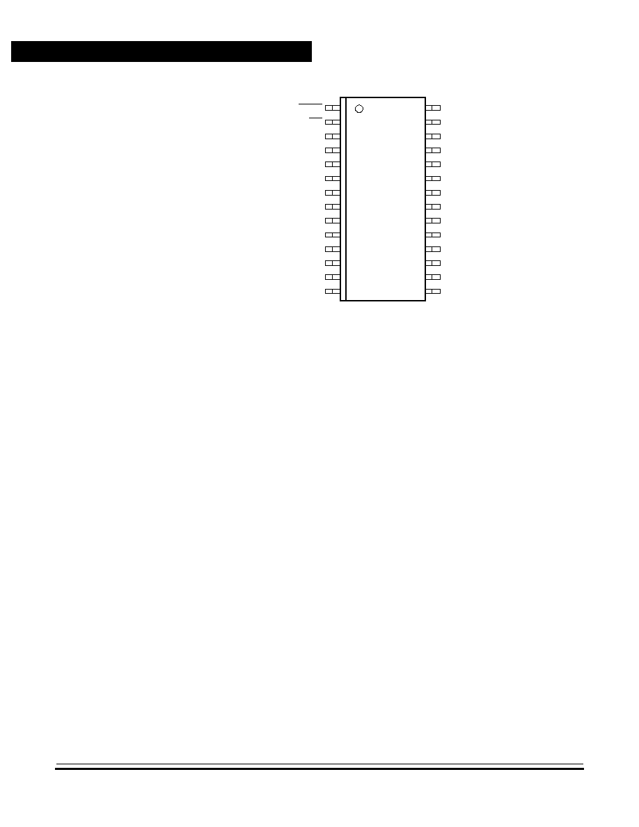
The pinout is shown in
Figure 1-2
.
NON-DISCLOSURE AGREEMENT REQUIRED
General Description
Technical Data
MC68HC05P18A
20
General Description
MOTOROLA
Figure 1-2. User Mode Pinout
1.5.1 Power Supply (V
DD
and V
SS
)
Power is supplied to the MCU through V
DD
and V
SS
. V
DD
is connected
to a regulated +5-volt supply and V
SS
is connected to ground.
Very fast signal transitions occur on the MCU pins. The short rise and
fall times place very high short-duration current demands on the power
supply. To prevent noise problems, take special care to provide good
power supply bypassing at the MCU. Use bypass capacitors with good
high-frequency characteristics and position them as close to the MCU as
possible. Bypassing requirements vary, depending on how heavily the
MCU pins are loaded.
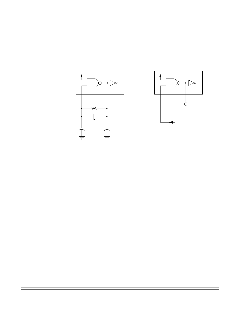
1.5.2 Oscillator Pins (OSC1 and OSC2)
The OSC1 and OSC2 pins are the control connections for the on-chip
oscillator. The OSC1 and OSC2 pins can accept:
1. A crystal or ceramic resonator, as shown in
Figure 1-3
(a)
2. An external clock signal, as shown in
Figure 1-3
(b)
1
2
3
4
5
6
7
8
9
10
11
12
13
14
28
27
26
25
24
23
22
21
20
19
18
17
16
15
RESET
IRQ
PA7
PA6
PA5
PA4
PA3
PA2
PA1
PA0
SDO/PB5
SDI/PB6
SCK/PB7
V
SS
V
DD
OSC1
OSC2
PD7/TCAP
TCMP
PD5/CKOUT
PC0
PC1
PC2
PC3/AD3
PC4/AD2
PC5/AD1
PC6/AD0
PC7/V
REFH
General Description
Functional Pin Description
MC68HC05P18A
Technical Data
MOTOROLA
General Description
21
NON-DISCLOSURE AGREEMENT REQUIRED
The frequency, f
OSC
, of the oscillator or external clock source is divided
by two to produce the internal PH2 bus clock operating frequency, f
OP
.
The oscillator cannot be turned off by software if the stop-to-halt
conversion is enabled via mask option.
Figure 1-3. Oscillator Connections
1.5.2.1 Crystal
The circuit in
Figure 1-3
(a) shows a typical oscillator circuit for an
AT-cut, parallel resonant crystal.
NOTE:
The crystal manufacturer's recommendations should be followed, as the
crystal parameters determine the external component values required to
provide maximum stability and reliable startup.
The load capacitance values used in the oscillator circuit design should
include all stray capacitances. Mount the crystal and components as
close as possible to the pins for startup stabilization and to minimize
output distortion.
TO V
DD
OR STOP
TO V
DD
OR STOP
(a)
Crystal or Ceramic
Resonator Connections
(b)
External Clock Source
Connections
OSC1
OSC2
MCU
37 pF
37 pF
4.7 M
MCU
OSC1
OSC2
UNCONNECTED
EXTERNAL CLOCK

NON-DISCLOSURE AGREEMENT REQUIRED
General Description
Technical Data
MC68HC05P18A
22
General Description
MOTOROLA
1.5.2.2 Ceramic Resonator
In cost-sensitive applications, a ceramic resonator can be used in place
of the crystal. The circuit in
Figure 1-3
(a) can be used for a ceramic
resonator.
NOTE:
The crystal manufacturer's recommendations should be followed, as the
crystal parameters determine the external component values required to
provide maximum stability and reliable startup.
The load capacitance values used in the oscillator circuit design should
include all stray capacitances. Mount the resonator and components as
close as possible to the pins for startup stabilization and to minimize
output distortion.
1.5.2.3 External Clock
An external clock from another CMOS-compatible device can be
connected to the OSC1 input, with the OSC2 input not connected, as
shown in
Figure 1-3
(b).
1.5.3 Reset (RESET)
Driving this input low resets the MCU to a known startup state. As an
output pin, the RESET pin indicates that an internal MCU reset has
occurred. The RESET pin contains an internal Schmitt trigger to improve
its noise immunity. Refer to
Section 5. Resets
.
1.5.4 Port A (PA0≠PA7)
Port A is comprised of eight I/O pins (PA0≠PA7). The state of any pin is
software programmable and all port A lines are configured as inputs
during power-on or reset. Eight mask options can be chosen to enable
pullups and interrupts (active low) on port A pins (see
1.4 Mask
Options
). Refer to
Section 7. Input/Output (I/O) Ports
and
Section 4.
Interrupts
.

General Description
Functional Pin Description
MC68HC05P18A
Technical Data
MOTOROLA
General Description
23
NON-DISCLOSURE AGREEMENT REQUIRED
1.5.5 Port B (PB5/SDO, PB6/SDI, and PB7/SCK)
Port B is comprised of three I/O pins which are shared with the SIOP
communications subsystem. The state of any pin is software
programmable and all port B lines are configured as inputs during
power-on or reset. Refer to
Section 7. Input/Output (I/O) Ports
and
Section 9. Serial Input/Output Ports (SIOP)
.
1.5.6 Port C (PC0≠PC2, PC3/AD3, PC4/AD2, PC5/AD1, PC6/AD0, and PC7/V
REFH
)
Port C is comprised of eight I/O pins which are shared with the A/D
converter subsystem. The state of any pin is software programmable
and all port C lines are configured as inputs during power-on or reset.
Port pins PC0 and PC1 are capable of sourcing and sinking high
currents. Refer to
Section 7. Input/Output (I/O) Ports
.
1.5.7 Port D (PD5/CKOUT and PD7/TCAP)
Port D is comprised of two I/O pins and one of them is shared with the
16-bit timer subsystem. The state of PD5/CKOUT is software
programmable and is configured as an input during power-on or reset.
PD7 is always an input; it may be read at any time, regardless of the
mode of operation the 16-bit timer may be in. Refer to
Section 7.
Input/Output (I/O) Ports
and
Section 8. 16-Bit Timer
.
NOTE:
A mask option turns the PD5/CKOUT pin into a clock output which is a
buffered OSC2 signal with a CMOS output driver. The clock output or the
port D function must be chosen with the mask option and is not alterable
in software.
1.5.8 Timer Output Compare (TCMP)
TCMP is the output from the 16-bit timer's output compare function. It is
low after reset. Refer to
Section 8. 16-Bit Timer
.

NON-DISCLOSURE AGREEMENT REQUIRED
General Description
Technical Data
MC68HC05P18A
24
General Description
MOTOROLA
1.5.9 Maskable Interrupt Request (IRQ)
This input pin drives the asynchronous interrupt function of the MCU.
The MCU completes the current instruction being executed before it
responds to the IRQ interrupt request. When IRQ is driven low, the event
is latched internally to signify an interrupt has been requested. When the
MCU completes its current instruction, the interrupt latch is tested. If the
interrupt latch is set, and the interrupt mask bit (I bit) in the condition
code register (CCR) is clear, the MCU begins the interrupt sequence.
Depending on the mask option selected, the IRQ pin triggers this
interrupt on either a negative going edge at the IRQ pin and/or while the
IRQ pin is held in the low state. In either case, the IRQ pin must be held
low for at least one t
ILIH
time period.
If the edge- and level-sensitive mask option is selected, the IRQ input
requires an external resistor connected to V
DD
for a wired-OR operation.
If the IRQ pin is not used, it must be tied to the V
DD
supply. The IRQ pin
contains an internal Schmitt trigger as part of its input circuitry to improve
noise immunity. Refer to
Section 4. Interrupts
.
1.5.10 CPU Core
The MC68HC05P18A uses a standard M68HC05 series CPU core. A
description of the instruction set is in
Section 12. Instruction Set
.

MC68HC05P18A
Technical Data
MOTOROLA
Memory Map
25
NON-DISCLOSURE AGREEMENT REQUIRED
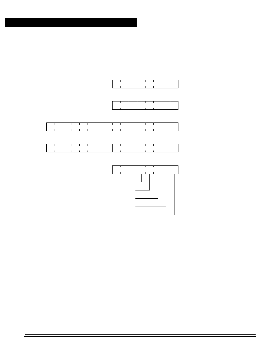
Technical Data -- MC68HC05P18A
Section 2. Memory Map
2.1 Contents
2.2
Introduction . . . . . . . . . . . . . . . . . . . . . . . . . . . . . . . . . . . . . . . .25
2.3
User Mode Memory Map . . . . . . . . . . . . . . . . . . . . . . . . . . . . .26
2.4
I/O and Control Registers . . . . . . . . . . . . . . . . . . . . . . . . . . . . .26
2.5
RAM . . . . . . . . . . . . . . . . . . . . . . . . . . . . . . . . . . . . . . . . . . . . .32
2.6
ROM . . . . . . . . . . . . . . . . . . . . . . . . . . . . . . . . . . . . . . . . . . . . .32
2.2 Introduction
The MC68HC05P18A utilizes 14 address lines to access an internal
memory space covering 16 Kbytes. This memory space is divided into:
∑
Input/output (I/O)
∑
Random-access memory (RAM)
∑
Electrically erasable programmable read-only memory
(EEPROM)
∑
Read-only memory (ROM)

NON-DISCLOSURE AGREEMENT REQUIRED
Memory Map
Technical Data
MC68HC05P18A
26
Memory Map
MOTOROLA
2.3 User Mode Memory Map
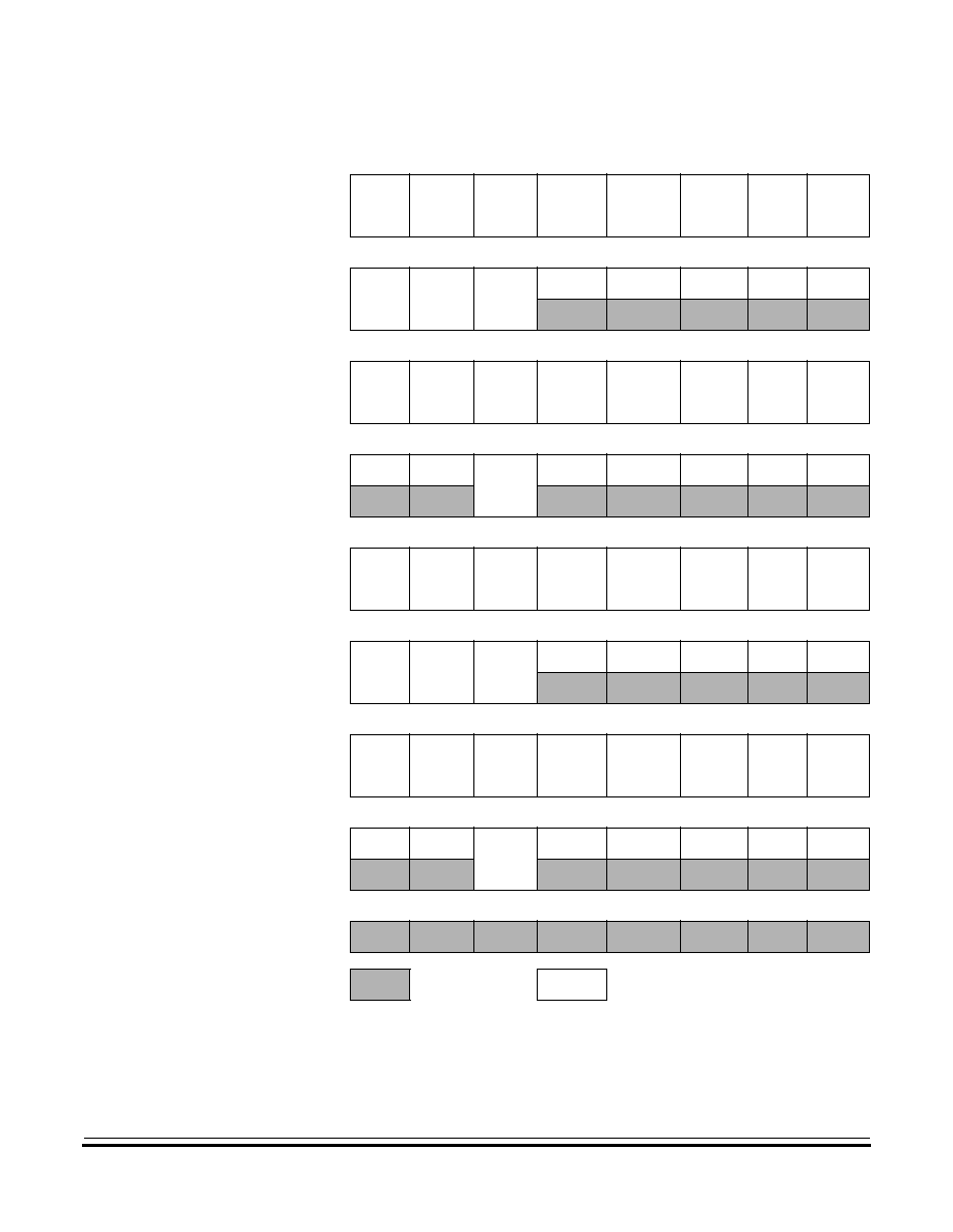
When the MC68HC05P18A is in user mode, these are active:
∑
32 bytes of I/O
∑
192 bytes of RAM
∑
128 bytes of EEPROM
∑
8000 bytes of user ROM
∑
48 bytes of user page zero ROM
∑
16 bytes of user vector ROM
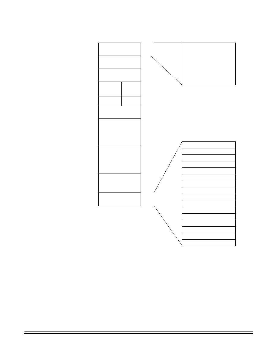
See
Figure 2-1
.
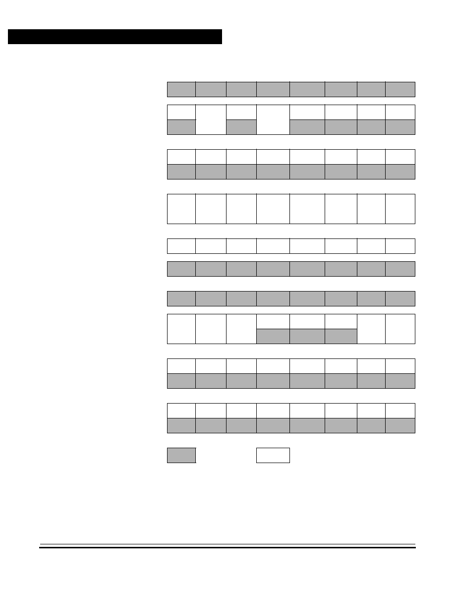
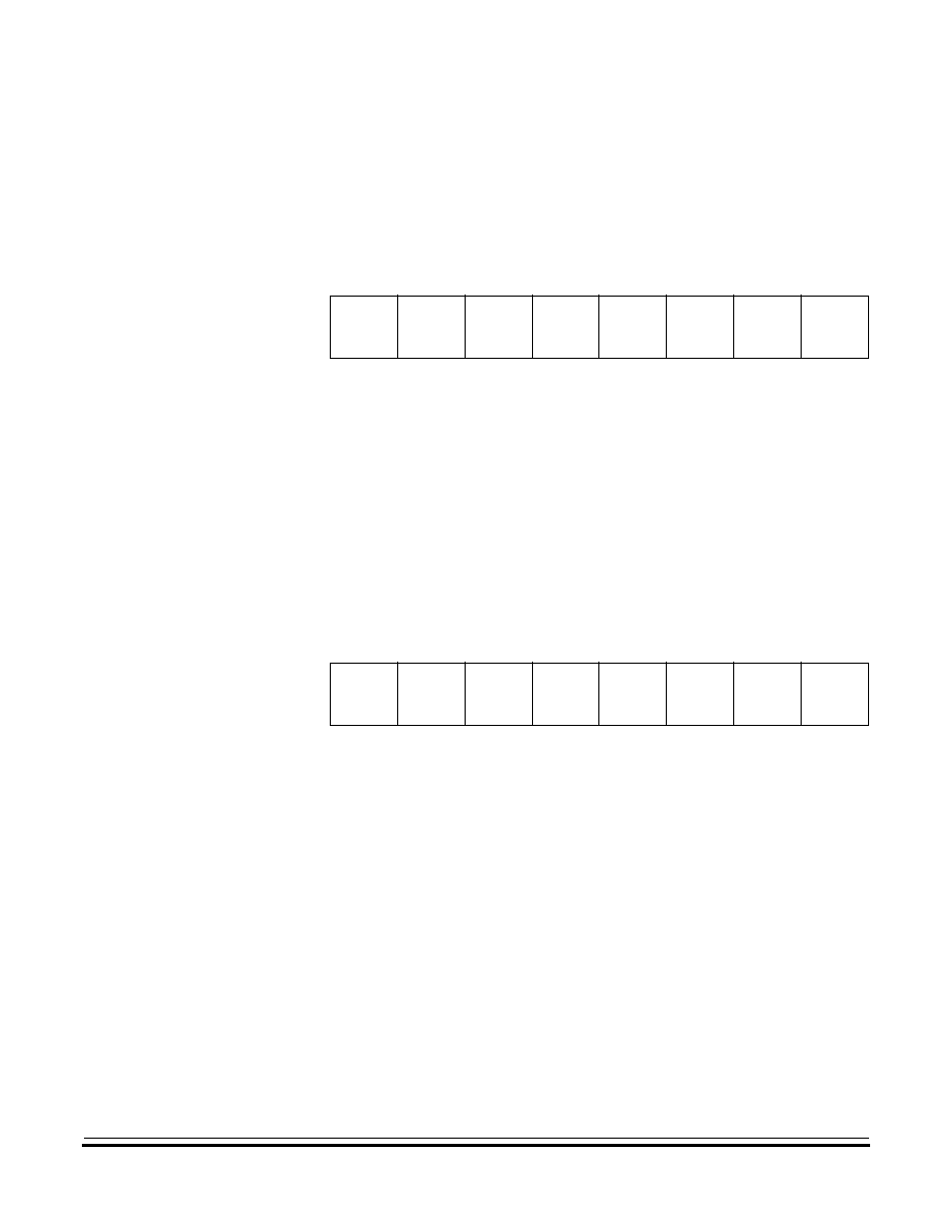
2.4 I/O and Control Registers
Figure 2-2
and
Figure 2-3
briefly describe the I/O and control registers
at locations $0000≠$001F.
NOTE:
Reading unimplemented bits returns unknown states, and writing
unimplemented bits is ignored.
Memory Map
I/O and Control Registers
MC68HC05P18A
Technical Data
MOTOROLA
Memory Map
27
NON-DISCLOSURE AGREEMENT REQUIRED
Figure 2-1. MC68HC05P18A User Mode Memory Map
0000
0031
0032
0079
0080
0191
0192
0255
0256
0271
0272
0399
0400
8127
8128
16127
16128
16367
16368
16383
$0000
$001F
$0020
$004F
$0050
$00BF
$00C0
$00FF
$0100
$010F
$0140
$01BF
$01C0
$1FBF
$1FC0
$3EFF
$3F00
$3FEF
$3FF0
$3FFF
RESET VECTOR (LOW BYTE)
RESET VECTOR (HIGH BYTE)
SWI VECTOR (LOW BYTE)
SWI VECTOR (HIGH BYTE)
IRQ VECTOR (LOW BYTE)
IRQ VECTOR (HIGH BYTE)
TIMER VECTOR (LOW BYTE)
TIMER VECTOR (HIGH BYTE)
UNIMPLEMENTED
UNIMPLEMENTED
$3FF6
$3FF7
$3FF8
$3FF9
$3FFA
$3FFB
$3FFC
$3FFD
$3FFE
$3FFF
UNIMPLEMENTED
$3FF5
UNIMPLEMENTED
$3FF4
UNIMPLEMENTED
$3FF3
UNIMPLEMENTED
$3FF2
UNIMPLEMENTED
$3FF1
COP CONTROL REGISTER
$3FF0
$001F
$0000
STACK
64 BYTES
INTERNAL RAM
192 BYTES
I/O
32 BYTES
USER VECTORS ROM
16 BYTES
RESERVED FOR
TEST
240 BYTES
USER ROM
8000 BYTES
USER ROM
48 BYTES
I/O REGISTERS
SEE
FIGURE 2-2
EEPROM
128 BYTES
UNUSED
7728 BYTES
NON-DISCLOSURE AGREEMENT REQUIRED
Memory Map
Technical Data
MC68HC05P18A
28
Memory Map
MOTOROLA
Figure 2-2. MC68HC05P18A I/O and Control Registers
Memory Map
PORT A DATA REGISTER
$0000
PORT B DATA REGISTER
$0001
PORT C DATA REGISTER
$0002
PORT D DATA REGISTER
$0003
PORT A DATA DIRECTION REGISTER
$0004
PORT B DATA DIRECTION REGISTER
$0005
PORT C DATA DIRECTION REGISTER
$0006
PORT D DATA DIRECTION REGISTER
$0007
UNIMPLEMENTED
$0008
UNIMPLEMENTED
$0009
SIOP CONTROL REGISTER
$000A
SIOP STATUS REGISTER
$000B
SIOP DATA REGISTER
$000C
UNIMPLEMENTED
$000D
UNIMPLEMENTED
$000E
UNIMPLEMENTED
$000F
UNIMPLEMENTED
$0010
UNIMPLEMENTED
$0011
TIMER CONTROL REGISTER
$0012
TIMER STATUS REGISTER
$0013
INPUT CAPTURE MSB
$0014
INPUT CAPTURE LSB
$0015
OUTPUT COMPARE MSB
$0016
OUTPUT COMPARE LSB
$0017
TIMER MSB
$0018
TIMER LSB
$0019
ALTERNATE COUNTER MSB
$001A
ALTERNATE COUNTER LSB
$001B
EEPROM PROGRAMMING REGISTER
$001C
A/D CONVERTER DATA REGISTER
$001D
A/D CONVERTER CONTROL & STATUS REGISTER
$001E
RESERVED FOR TEST
$001F
Memory Map
I/O and Control Registers
MC68HC05P18A
Technical Data
MOTOROLA
Memory Map
29
NON-DISCLOSURE AGREEMENT REQUIRED
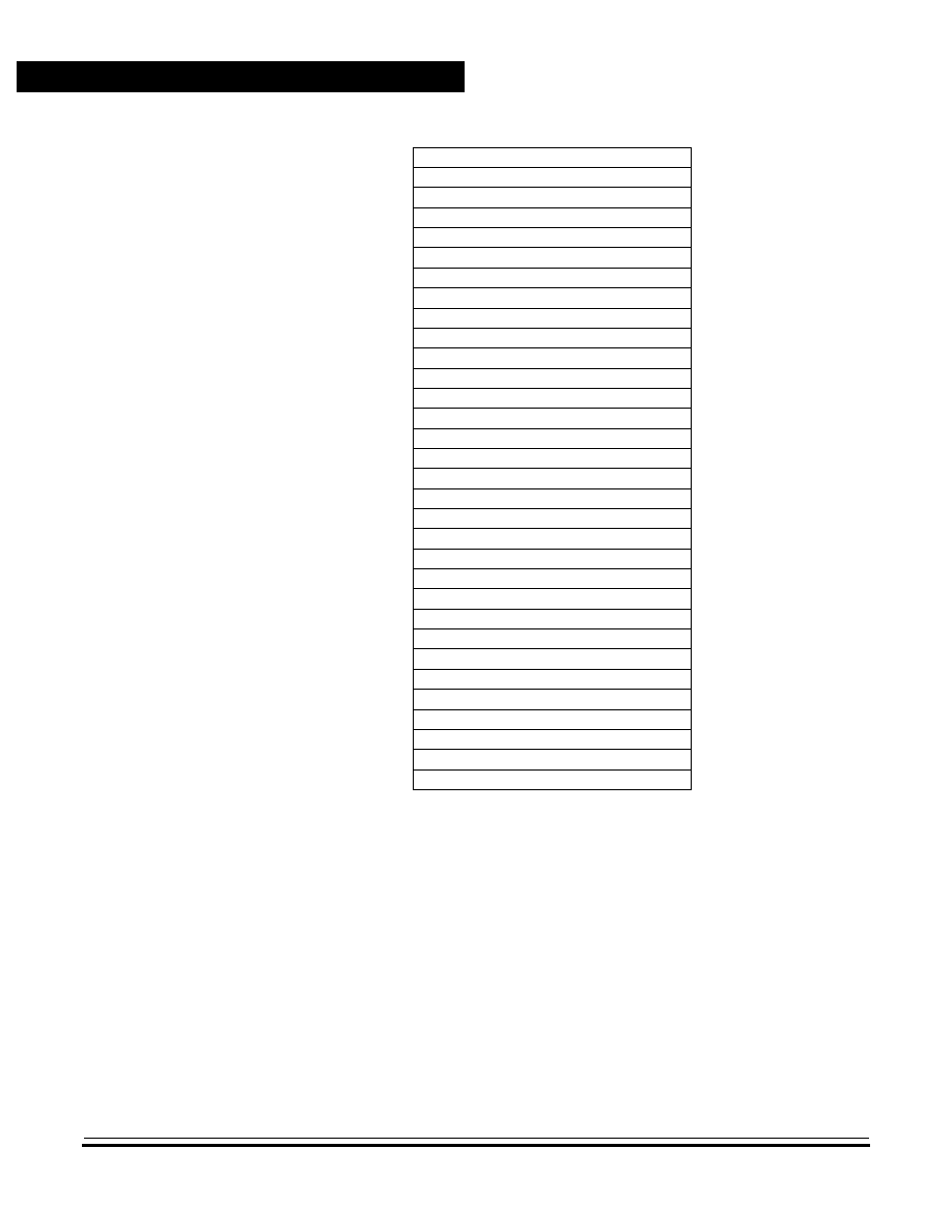
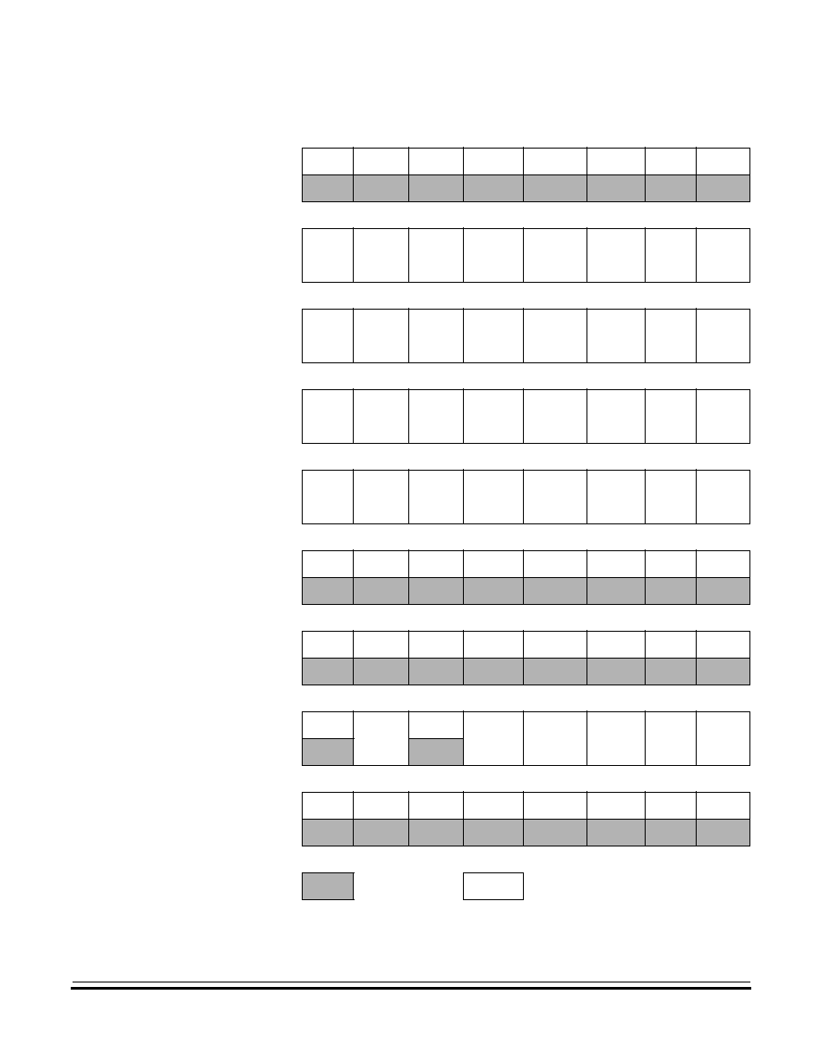
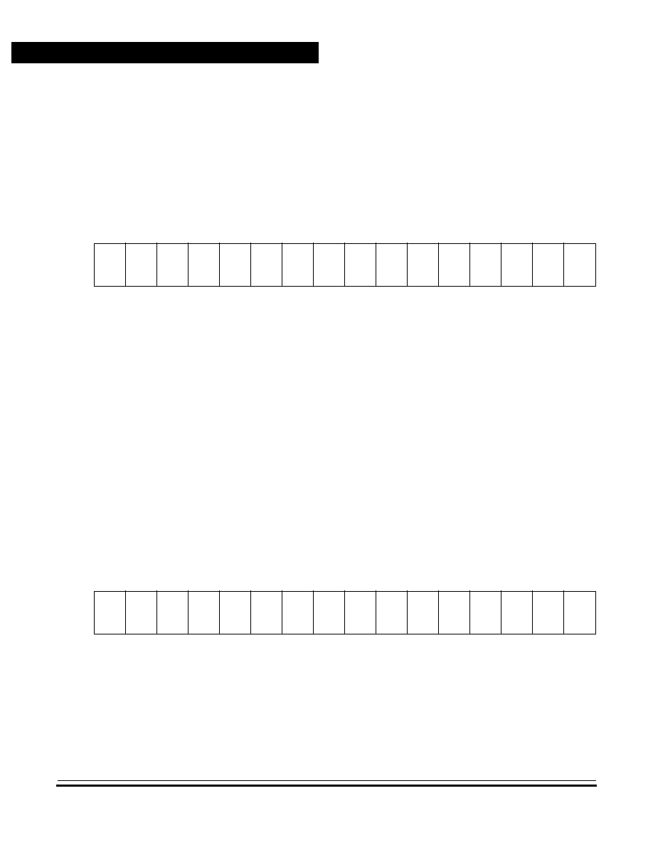
Addr.
Register Name
Bit 7
6
5
4
3
2
1
Bit 0
$0000
Port A Data Register
(PORTA)
See page 56.
Read:
PA7
PA6
PA5
PA4
PA3
PA2
PA1
PA0
Write:
Reset:
Unaffected by reset
$0001
Port B Data Register
(PORTB)
See page 57.
Read:
PB7
PB6
PB5
0
0
0
0
0
Write:
Reset:
Unaffected by reset
$0002
Port C Data Register
(PORTC)
See page 58.
Read:
PC7
PC6
PC5
PC4
PC3
PC2
PC1
PC0
Write:
Reset:
Unaffected by reset
$0003
Port D Data Register
(PORTD)
See page 59.
Read:
PD7
0
PD5
1
0
0
0
0
Write:
Reset:
Unaffected by reset
$0004
Port A Data Direction
(DDRA)
See page 56.
Read:
DDRA7
DDRA6
DDRA5
DDRA4
DDRA3
DDRA2
DDRA1
DDRA0
Write:
Reset:
0
0
0
0
0
0
0
0
$0005
Port B Data Direction
(DDRB)
See page 57.
Read:
DDRB7
DDRB6
DDRB5
1
1
1
1
1
Write:
Reset:
0
0
0
0
0
0
0
0
$0006
Port C Data Direction
(DDRC)
See page 58.
Read:
DDRC7
DDRC6
DDRC5
DDRC4
DDRC3
DDRC2
DDRC1
DDRC0
Write:
Reset:
0
0
0
0
0
0
0
0
$0007
Port D Data Direction
(DDRD)
See page 59.
Read:
0
0
DDRD5
0
0
0
0
0
Write:
Reset:
0
0
0
0
0
0
0
0
$0008
Unimplemented
= Unimplemented
R
= Reserved
U = Unaffected
Figure 2-3. I/O and Control Registers (Sheet 1 of 4)
NON-DISCLOSURE AGREEMENT REQUIRED
Memory Map
Technical Data
MC68HC05P18A
30
Memory Map
MOTOROLA
$0009
Unimplemented
$000A
SIOP Control Register
(SCR)
See page 80.
Read:
0
SPE
0
MSTR
0
0
0
0
Write:
Reset:
0
0
0
0
0
0
0
0
$000B
SIOP Status Register
(SSR)
See page 82.
Read:
SPIF
DCOL
0
0
0
0
0
0
Write:
Reset:
0
0
0
0
0
0
0
0
$000C
SIOP Data Register
(SDR)
See page 83.
Read:
SDR7
SDR6
SDR5
SDR4
SDR3
SDR2
SDR1
SDR0
Write:
Reset:
Unaffected by reset
$000D
Reserved
R
R
R
R
R
R
R
R
$000E
Unimplemented
$0011
Unimplemented
$0012
Timer Control Register
(TCR)
See page 72.
Read:
ICIE
OCIE
TOIE
0
0
0
IEDG
OLVL
Write:
Reset:
0
0
0
0
0
0
U
0
$0013
Timer Status Register
(TSR)
See page 73.
Read:
ICF
OCF
TOF
0
0
0
0
0
Write:
Reset:
U
U
U
0
0
0
0
0
$0014
Input Capture Register
(ICRH)
See page 70.
Read: ICRH7
ICRH6
ICRH5
ICRH4
ICRH3
ICRH2
ICRH1
ICRH0
Write:
Reset:
Unaffected by reset
Addr.
Register Name
Bit 7
6
5
4
3
2
1
Bit 0
= Unimplemented
R
= Reserved
U = Unaffected
Figure 2-3. I/O and Control Registers (Sheet 2 of 4)
Memory Map
I/O and Control Registers
MC68HC05P18A
Technical Data
MOTOROLA
Memory Map
31
NON-DISCLOSURE AGREEMENT REQUIRED
$0015
Input Capture Register
(ICRL)
See page 70.
Read:
ICRL7
ICRL6
ICRL5
ICRL4
ICRL3
ICRL2
ICRL1
ICRL0
Write:
Reset:
Unaffected by reset
$0016
Output Compare Register
(OCRH)
See page 68.
Read:
OCRH7
OCRH6
OCRH5
OCRH4
OCRH3
OCRH2
OCRH1
OCRH0
Write:
Reset:
Unaffected by reset
$0017
Output Compare Register
(OCRL)
See page 68.
Read:
OCRL7
OCRL6
OCRL5
OCRL4
OCRL3
OCRL2
OCRL1
OCRL0
Write:
Reset:
Unaffected by reset
$0018
Timer Counter Register
(TMRH)
See page 66.
Read:
TMRH7
TMRH6
TMRH5
TMRH4
TMRH3
TMRH2
TMRH1
TMRH0
Write:
Reset:
1
1
1
1
1
1
1
1
$0019
Timer Counter Register
(TMRL)
See page 66.
Read:
TMRL7
TMRL6
TMRL5
TMRL4
TMRL3
TMRL2
TMRL1
TMRL0
Write:
Reset:
1
1
1
1
1
1
1
1
$001A
Alternate Counter Register
(ACRH)
See page 66.
Read: ACRH7
ACRH6
ACRH5
ACRH4
ACRH3
ACRH2
ACRH1
ACRH0
Write:
Reset:
1
1
1
1
1
1
1
1
$001B
Alternate Counter Register
(ACRL)
See page 66.
Read: ACRL7
ACRL6
ACRL5
ACRL4
ACRL3
ACRL2
ACRL1
ACRL0
Write:
Reset:
1
1
1
1
1
1
1
1
$001C
EEPROM Programming
Register (EEPROG)
See page 86.
Read:
0
CPEN
0
ER1
ER0
LATCH
EERC
EEPGM
Write:
Reset:
0
0
0
0
0
0
0
0
$001D
A/D Conversion Value Data
Register (ADC)
See page 96.
Read:
AD7
AD6
AD5
AD4
AD3
AD2
AD1
AD0
Write:
Reset:
Unaffected by reset
Addr.
Register Name
Bit 7
6
5
4
3
2
1
Bit 0
= Unimplemented
R
= Reserved
U = Unaffected
Figure 2-3. I/O and Control Registers (Sheet 3 of 4)
NON-DISCLOSURE AGREEMENT REQUIRED
Memory Map
Technical Data
MC68HC05P18A
32
Memory Map
MOTOROLA
2.5 RAM
The user RAM consists of 192 bytes (including the stack) at locations
$0050≠$010F. The stack begins at address $00FF. The stack pointer
can access 64 bytes of RAM from $00FF to $00C0.
NOTE:
Using the stack area for data storage or temporary work locations
requires care to prevent it from being overwritten due to stacking from an
interrupt or subroutine call.
2.6 ROM
There are 8064 bytes of user ROM available, consisting of:
∑
8000 bytes at locations $1FC0≠$3EFF
∑
48 bytes in page zero locations $0020≠$004F
∑
16 additional bytes for user vectors at locations $3FF0≠$3FFF
NOTE:
Address space $3F00≠$3FEF is reserved for test code. Unlike other
M68HC05 devices, the MC68HC05P18A does not contain self-check
code.
$001E
A/D Converter Status and
Control Register (ADSCR)
See page 94.
Read:
CC
R
ADON
0
0
CH2
CH1
CH0
Write:
Reset:
0
0
0
0
0
0
0
0
$001F
Reserved
R
R
R
R
R
R
R
R
Addr.
Register Name
Bit 7
6
5
4
3
2
1
Bit 0
= Unimplemented
R
= Reserved
U = Unaffected
Figure 2-3. I/O and Control Registers (Sheet 4 of 4)

MC68HC05P18A
Technical Data
MOTOROLA
Central Processor Unit (CPU)
33
NON-DISCLOSURE AGREEMENT REQUIRED
Technical Data -- MC68HC05P18A
Section 3. Central Processor Unit (CPU)
3.1 Contents
3.2
Introduction . . . . . . . . . . . . . . . . . . . . . . . . . . . . . . . . . . . . . . . .33
3.3
CPU Registers . . . . . . . . . . . . . . . . . . . . . . . . . . . . . . . . . . . . .34
3.3.1
Accumulator . . . . . . . . . . . . . . . . . . . . . . . . . . . . . . . . . . . . .35
3.3.2
Index Register . . . . . . . . . . . . . . . . . . . . . . . . . . . . . . . . . . .35
3.3.3
Stack Pointer . . . . . . . . . . . . . . . . . . . . . . . . . . . . . . . . . . . .35
3.3.4
Program Counter . . . . . . . . . . . . . . . . . . . . . . . . . . . . . . . . .36
3.3.5
Condition Code Register . . . . . . . . . . . . . . . . . . . . . . . . . . .37
3.4
Arithmetic/Logic Unit. . . . . . . . . . . . . . . . . . . . . . . . . . . . . . . . .38
3.2 Introduction
This section describes the central processor unit (CPU) registers.
NON-DISCLOSURE AGREEMENT REQUIRED
Central Processor Unit (CPU)
Technical Data
MC68HC05P18A
34
Central Processor Unit (CPU)
MOTOROLA
3.3 CPU Registers
Figure 3-1
shows the five CPU registers. CPU registers are not part of
the memory map.
Figure 3-1. Programming Model
ACCUMULATOR (A)
A
INDEX REGISTER (X)
X
SP
1
1
0
0
0
0
0
0
0
0
PCL
PCH
0
0
Z
C
I
N
1
H
1
1
0
4
7
5
CONDITION CODE REGISTER (CCR)
PROGRAM COUNTER (PC)
STACK POINTER (SP)
0
7
8
15
15
5
7
0
0
HALF-CARRY FLAG
INTERRUPT MASK
NEGATIVE FLAG
ZERO FLAG
CARRY/BORROW FLAG
10
6
Central Processor Unit (CPU)
CPU Registers
MC68HC05P18A
Technical Data
MOTOROLA
Central Processor Unit (CPU)
35
NON-DISCLOSURE AGREEMENT REQUIRED
3.3.1 Accumulator
The accumulator (A) is a general-purpose 8-bit register. The CPU uses
the accumulator to hold operands and results of arithmetic and non-
arithmetic operations.
3.3.2 Index Register
In the indexed addressing modes, the CPU uses the byte in the index
register (X) to determine the conditional address of the operand.
The 8-bit index register can also serve as a temporary data storage
location.
3.3.3 Stack Pointer
The stack pointer (SP) is a 16-bit register that contains the address of
the next location on the stack. During a reset or after the reset stack
pointer (RSP) instruction, the stack pointer is preset to $00FF. The
address in the stack pointer decrements as data is pushed onto the
stack and increments as data is pulled from the stack.
Bit 7
6
5
4
3
2
1
Bit 0
Read:
Write:
Reset:
Unaffected by reset
Figure 3-2. Accumulator (A)
Bit 7
6
5
4
3
2
1
Bit 0
Read:
Write:
Reset:
Unaffected by reset
Figure 3-3. Index Register (X)
NON-DISCLOSURE AGREEMENT REQUIRED
Central Processor Unit (CPU)
Technical Data
MC68HC05P18A
36
Central Processor Unit (CPU)
MOTOROLA
The 10 most significant bits of the stack pointer are permanently fixed at
000000011, so the stack pointer produces addresses from $00C0 to
$00FF. If subroutines and interrupts use more than 64 stack locations,
the stack pointer wraps around to address $00FF and begins writing
over the previously stored data. A subroutine uses two stack locations.
An interrupt uses five locations.
3.3.4 Program Counter
The program counter (PC) is a 16-bit register that contains the address
of the next instruction or operand to be fetched. The two most significant
bits of the program counter are ignored internally and appear as 00.
Normally, the address in the program counter automatically increments
to the next sequential memory location every time an instruction or
operand is fetched. Jump, branch, and interrupt operations load the
program counter with an address other than that of the next sequential
location.
Bit
15
14
13
12
11
10
9
8
7
6
5
4
3
2
1
Bit
0
Read:
Write:
Reset:
0
0
0
0
0
0
0
0
1
1
1
1
1
1
1
1
Figure 3-4. Stack Pointer (SP)
Bit
15
14
13
12
11
10
9
8
7
6
5
4
3
2
1
Bit
0
Read:
0
0
5
Write:
Reset:
0
0
Loaded with vectors from $3FF3 and $3FFF
Figure 3-5. Program Counter (PC)

Central Processor Unit (CPU)
CPU Registers
MC68HC05P18A
Technical Data
MOTOROLA
Central Processor Unit (CPU)
37
NON-DISCLOSURE AGREEMENT REQUIRED
3.3.5 Condition Code Register
The condition code register (CCR) is an 8-bit register whose three most
significant bits are permanently fixed at 111. The condition code register
contains the interrupt mask and four flags that indicate the results of the
instruction just executed. The following paragraphs describe the
functions of the condition code register.
Half-Carry Flag
The CPU sets the half-carry flag when a carry occurs between bits 3
and 4 of the accumulator during an ADD or ADC operation. The half-
carry flag is required for binary coded decimal (BCD) arithmetic
operations.
Interrupt Mask
Setting the interrupt mask disables interrupts. If an interrupt request
occurs while the interrupt mask is logic 0, the CPU saves the CPU
registers on the stack, sets the interrupt mask, and then fetches the
interrupt vector. If an interrupt request occurs while the interrupt mask
is set, the interrupt request is latched. Normally, the CPU processes
the latched interrupt as soon as the interrupt mask is cleared again.
A return-from-interrupt (RTI) instruction pulls the CPU registers from
the stack, restoring the interrupt mask to its cleared state. After any
reset, the interrupt mask is set and can be cleared only by a software
instruction.
Negative Flag
The CPU sets the negative flag when an arithmetic operation, logical
operation, or data manipulation produces a negative result.
Bit 7
6
5
4
3
2
1
Bit 0
Read:
1
1
1
H
I
N
Z
C
Write:
Reset:
1
1
1
U
1
U
U
U
= Unimplemented
U = Unaffected
Figure 3-6. Condition Code Register (CCR)

NON-DISCLOSURE AGREEMENT REQUIRED
Central Processor Unit (CPU)
Technical Data
MC68HC05P18A
38
Central Processor Unit (CPU)
MOTOROLA
Zero Flag
The CPU sets the zero flag when an arithmetic operation, logical
operation, or data manipulation produces a result of $00.
Carry/Borrow Flag
The CPU sets the carry/borrow flag when an addition operation
produces a carry out of bit 7 of the accumulator or when a subtraction
operation requires a borrow. Some logical operations and data
manipulation instructions also clear or set the carry/borrow flag.
3.4 Arithmetic/Logic Unit
The arithmetic/logic unit (ALU) performs the arithmetic and logical
operations defined by the instruction set.
The binary arithmetic circuits decode instructions and set up the ALU for
the selected operation. Most binary arithmetic is based on the addition
algorithm, carrying out subtraction as negative addition. Multiplication is
not performed as a discrete operation but as a chain of addition and shift
operations within the ALU. The multiply instruction (MUL) requires 11
internal clock cycles to complete this chain of operations.

MC68HC05P18A
Technical Data
MOTOROLA
Interrupts
39
NON-DISCLOSURE AGREEMENT REQUIRED
Technical Data -- MC68HC05P18A
Section 4. Interrupts
4.1 Contents
4.2
Introduction . . . . . . . . . . . . . . . . . . . . . . . . . . . . . . . . . . . . . . . .39
4.3
CPU Interrupt Processing . . . . . . . . . . . . . . . . . . . . . . . . . . . . .40
4.4
Interrupt Types . . . . . . . . . . . . . . . . . . . . . . . . . . . . . . . . . . . . .42
4.4.1
Reset Interrupt Sequence . . . . . . . . . . . . . . . . . . . . . . . . . .42
4.4.2
Software Interrupt (SWI). . . . . . . . . . . . . . . . . . . . . . . . . . . .42
4.4.3
Hardware Interrupts . . . . . . . . . . . . . . . . . . . . . . . . . . . . . . .43
4.4.3.1
External Interrupt (IRQ) . . . . . . . . . . . . . . . . . . . . . . . . . .43
4.4.3.2
Input Capture Interrupt . . . . . . . . . . . . . . . . . . . . . . . . . . .43
4.4.3.3
Output Compare Interrupt . . . . . . . . . . . . . . . . . . . . . . . .44
4.4.3.4
Timer Overflow Interrupt . . . . . . . . . . . . . . . . . . . . . . . . .44
4.2 Introduction
The MCU can be interrupted six different ways:
1. Non-maskable software interrupt instruction (SWI)
2. External asynchronous interrupt (IRQ)
3. Input capture interrupt (TIMER)
4. Output compare interrupt (TIMER)
5. Timer overflow interrupt (TIMER)
6. Port A interrupt, if selected as a mask option

NON-DISCLOSURE AGREEMENT REQUIRED
Interrupts
Technical Data
MC68HC05P18A
40
Interrupts
MOTOROLA
4.3 CPU Interrupt Processing
Interrupts cause the processor to save the register contents on the stack
and to set the interrupt mask (I bit) to prevent additional interrupts. Unlike
reset, hardware interrupts do not cause the current instruction execution
to be halted, but are considered pending until the current instruction is
completed.
When the current instruction is completed, the processor checks all
pending hardware interrupts. If interrupts are not masked (I bit in the
condition code register is clear), and the corresponding interrupt enable
bit is set, the processor proceeds with interrupt processing. Otherwise,
the next instruction is fetched and executed. The SWI is executed the
same as any other instruction, regardless of the I-bit state.
When an interrupt is to be processed, the CPU puts the register contents
on the stack, sets the I bit in the CCR, and fetches the address of the
corresponding interrupt service routine from the vector table at locations
$3FF0≠$3FFF. If more than one interrupt is pending when the interrupt
vector is fetched, the interrupt with the highest vector location, shown in
Table 4-1
, is serviced first.
A return-from-interrupt (RTI) instruction is used to signify when the
interrupt software service routine is completed. The RTI instruction
Table 4-1. Vector Address for Interrupts and Reset
Register
Flag
Name
Interrupts
CPU
Interrupt
Vector Address
N/A
N/A
Reset
RESET
$3FFE≠$3FFF
N/A
N/A
Software
SWI
$3FFC≠$3FFD
N/A
N/A
External interrupt
IRQ
$3FFA≠$3FFB
TSR
ICF
Timer input capture
TIMER
$3FF8≠$3FF9
TSR
OCF
Timer output compare
TIMER
$3FF8≠$3FF9
TSR
TOF
Timer overflow
TIMER
$3FF8≠$3FF9
N/A
N/A
Unimplemented
N/A
$3FF6≠$3FF7
N/A
N/A
Unimplemented
N/A
$3FF4≠$3FF5
N/A
N/A
Unimplemented
N/A
$3FF2≠$3FF3
N/A
N/A
Unimplemented
N/A
$3FF0≠$3FF1

Interrupts
CPU Interrupt Processing
MC68HC05P18A
Technical Data
MOTOROLA
Interrupts
41
NON-DISCLOSURE AGREEMENT REQUIRED
causes the CPU state to be recovered from the stack and normal
processing to resume at the next instruction that was to be executed
when the interrupt took place.
Figure 4-1
shows the sequence of events
that occur during interrupt processing.
Figure 4-1. Interrupt Processing Flowchart
IS I BIT
SET?
FROM RESET
LOAD PC FROM
SWI: $3FFC AND $3FFD
IRQ: $3FFA≠$3FFB
TIMER: $3FF8≠$3FF9
SET
I BIT IN CCR
STACK
PC, X, A, CC
CLEAR IRQ
REQUEST
LATCH
RESTORE REGISTERS
FROM STACK
CC, A, X, PC
Y
N
EXECUTE INSTRUCTION
FETCH NEXT INSTRUCTION
IRQ
INTERRUPT?
Y
N
TIMER
INTERRUPT?
Y
N
SWI
INSTRUCTION?
Y
N
RTI
INSTRUCTION?
Y
N

NON-DISCLOSURE AGREEMENT REQUIRED
Interrupts
Technical Data
MC68HC05P18A
42
Interrupts
MOTOROLA
4.4 Interrupt Types
The interrupts fall into these three categories which are discussed here:
∑
Reset interrupt sequence
∑
Software interrupt (SWI)
∑
Hardware interrupts
4.4.1 Reset Interrupt Sequence
The reset function is not in the strictest sense an interrupt; however, it is
acted upon in a similar manner as shown in
Figure 4-1
. A low-level input
on the RESET pin or internally generated RST signal causes:
∑
The program to vector to its starting address, which is specified by
the contents of memory locations $3FFE and $3FFF
∑
The I bit in the condition code register (CCR) to be set
∑
The MCU to be configured to a known state as described in
Section 5. Resets
.
4.4.2 Software Interrupt (SWI)
The SWI is an executable instruction. It is also a non-maskable interrupt
since it is executed regardless of the state of the I bit in the CCR. As with
any instruction, interrupts pending during the previous instruction are
serviced before the SWI opcode is fetched. The interrupt service routine
address for the SWI instruction is specified by the contents of memory
locations $3FFC and $3FFD.

Interrupts
Interrupt Types
MC68HC05P18A
Technical Data
MOTOROLA
Interrupts
43
NON-DISCLOSURE AGREEMENT REQUIRED
4.4.3 Hardware Interrupts
All hardware interrupts are maskable by the I bit in the CCR. If the I bit
is set, all hardware interrupts (internal and external) are disabled.
Clearing the I bit enables the hardware interrupts.
The four hardware interrupts are explained here:
∑
External interrupt (IRQ)
∑
Input capture interrupt
∑
Output compare interrupt
∑
Timer overflow interrupt
4.4.3.1 External Interrupt (IRQ)
The IRQ pin drives an asynchronous interrupt to the CPU. An edge
detector flip-flop is latched on the falling edge of IRQ. If either the output
from the internal edge detector flip-flop or the level on the IRQ pin is low,
a request is synchronized to the CPU to generate the IRQ interrupt. If the
edge-sensitive only mask option is selected, the output of the internal
edge detector flip-flop is sampled and the input level on the IRQ pin is
ignored. If port A interrupts are selected as a mask option, a port A
interrupt uses the same vector. The interrupt service routine address is
specified by the contents of memory locations $3FFA and $3FFB.
NOTE:
The internal interrupt latch is cleared 9 PH2 clock cycles after the
interrupt is recognized (after location $3FFA is read). Therefore, another
external interrupt pulse could be latched during the IRQ service routine.
When the edge- and level-sensitive mask option is selected, the voltage
applied to the IRQ pin must return to the high state before the return-
from-interrupt (RTI) instruction in the interrupt service routine is
executed.
4.4.3.2 Input Capture Interrupt
The input capture interrupt is generated by the 16-bit timer as described
in
Section 8. 16-Bit Timer
. The input capture interrupt flag is located in

NON-DISCLOSURE AGREEMENT REQUIRED
Interrupts
Technical Data
MC68HC05P18A
44
Interrupts
MOTOROLA
the timer status register (TSR) and its corresponding enable bit can be
found in the timer control register (TCR).
The I bit in the CCR must be clear in order for the input capture interrupt
to be enabled. The interrupt service routine address is specified by the
contents of memory locations $3FF8 and $3FF9.
4.4.3.3 Output Compare Interrupt
The output compare interrupt is generated by the 16-bit timer as
described in
Section 8. 16-Bit Timer
. The output compare interrupt flag
is located in register TSR and its corresponding enable bit can be found
in register TCR.
The I bit in the CCR must be clear in order for the output compare
interrupt to be enabled. The interrupt service routine address is specified
by the contents of memory locations $3FF8 and $3FF9.
4.4.3.4 Timer Overflow Interrupt
The timer overflow interrupt is generated by the 16-bit timer as described
in
Section 8. 16-Bit Timer
. The timer overflow interrupt flag is located in
register TSR and its corresponding enable bit can be found in register
TCR.
The I bit in the CCR must be clear in order for the timer overflow interrupt
to be enabled. This internal interrupt will vector to the interrupt service
routine located at the address specified by the contents of memory
locations $3FF8 and $3FF9.

MC68HC05P18A
Technical Data
MOTOROLA
Resets
45
NON-DISCLOSURE AGREEMENT REQUIRED
Technical Data -- MC68HC05P18A
Section 5. Resets
5.1 Contents
5.2
Introduction . . . . . . . . . . . . . . . . . . . . . . . . . . . . . . . . . . . . . . . .45
5.3
External Reset (RESET). . . . . . . . . . . . . . . . . . . . . . . . . . . . . .46
5.4
Internal Resets . . . . . . . . . . . . . . . . . . . . . . . . . . . . . . . . . . . . .46
5.4.1
Power-On Reset (POR) . . . . . . . . . . . . . . . . . . . . . . . . . . . .47
5.4.2
Computer Operating Properly (COP) Reset . . . . . . . . . . . . .47
5.4.3
Low-Voltage Reset (LVR). . . . . . . . . . . . . . . . . . . . . . . . . . .48
5.2 Introduction
The MCU can be reset from four sources:
∑
One external input
∑
Three internal reset conditions
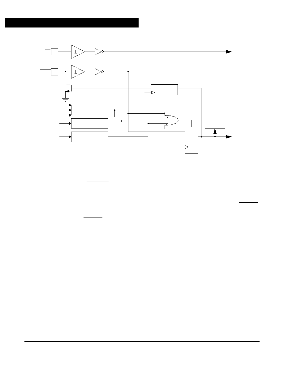
The RESET pin is an input with a Schmitt trigger as shown in
Figure 5-1
. The CPU and all peripheral modules are reset by the internal
reset signal (RST), which is the logical OR of internal reset functions and
is clocked by PH2.
NON-DISCLOSURE AGREEMENT REQUIRED
Resets
Technical Data
MC68HC05P18A
46
Resets
MOTOROLA
Figure 5-1. Reset Block Diagram
5.3 External Reset (RESET)
The RESET input is the only external reset and is connected to an
internal Schmitt trigger. The external reset occurs whenever the RESET
input is driven below the lower threshold and remains in reset until the
RESET pin rises above the upper threshold. The upper and lower
thresholds are given in
Section 13. Electrical Specifications
.
5.4 Internal Resets
The three internally generated resets are:
∑
Initial power-on reset (POR)
∑
Computer operating properly (COP) watchdog timer
∑
Low-voltage reset (LVR)
CPU
LATCH
RESET
COP WATCHDOG
(COPR)
RST
OSC
DATA
ADDRESS
PH2
TO OTHER
PERIPHERALS
S
LOW-VOLTAGE
RESET (LVR)
V
DD
TO IRQ
LOGIC
POWER-ON RESET
(POR)
V
DD
PH2
CLOCKED
ONE-SHOT
PULSE WIDTH = 4 X E-CLK
D
IRQ

Resets
Internal Resets
MC68HC05P18A
Technical Data
MOTOROLA
Resets
47
NON-DISCLOSURE AGREEMENT REQUIRED
5.4.1 Power-On Reset (POR)
The internal POR is generated at power-up to allow the clock oscillator
to stabilize. The POR is strictly for power turn-on conditions and should
not be used to detect a drop in the power supply voltage. There is a 4064
PH2 clock cycle oscillator stabilization delay after the oscillator becomes
active.
The POR generates the RST signal and resets the MCU. At the same
time, the POR pulls the RESET pin low allowing external devices to be
reset with the MCU. If any other reset function is active at the end of this
4064 PH2 clock cycle delay, the RST signal remains active until the
other reset condition(s) end.
5.4.2 Computer Operating Properly (COP) Reset
When the COP watchdog timer is enabled by mask option, the internal
COP reset is generated automatically by a timeout of the COP watchdog
timer. This timer is implemented with an 18-stage ripple counter that
provides a timeout period of 65.5 ms when a 4-MHz oscillator is used.
The COP watchdog counter is cleared by writing a logical 0 to bit 0 at
location $3FF0.
The COP register is shared with the most-significant bit (MSB) of an
unimplemented user interrupt vector, as shown in
Figure 5-2
. Reading
this location returns the MSB of the unimplemented user interrupt vector.
Writing to this location clears the COP watchdog timer.
Address:
$3FF0
Bit 7
6
5
4
3
2
1
Bit 0
Read:
0
0
0
0
0
0
0
0
Write:
R
COPR
Reset:
Unaffected by reset
R
= Reserved
= Unimplemented
Figure 5-2. COP Register (COPR)

NON-DISCLOSURE AGREEMENT REQUIRED
Resets
Technical Data
MC68HC05P18A
48
Resets
MOTOROLA
5.4.3 Low-Voltage Reset (LVR)
The internal LVR reset is generated when the supply voltage to the V
DD
pin falls below a nominal 3.80 Vdc. The LVR threshold is not intended to
be an accurate and stable trip point, but is intended to assure that the
CPU is held in reset when the V
DD
supply voltage is below reasonable
operating limits. If the LVR is tripped for a short time, the LVR reset
signal will last at least two cycles of the CPU bus clock, PH2. A mask
option is provided to disable the LVR.
The LVR generates the RST signal, which resets the CPU and other
peripherals. If any other reset function is active at the end of the LVR
reset signal, the RST signal remains in the reset condition until the other
reset condition(s) end.

MC68HC05P18A
Technical Data
MOTOROLA
Operating Modes
49
NON-DISCLOSURE AGREEMENT REQUIRED
Technical Data -- MC68HC05P18A
Section 6. Operating Modes
6.1 Contents
6.2
Introduction . . . . . . . . . . . . . . . . . . . . . . . . . . . . . . . . . . . . . . . .49
6.3
User Mode . . . . . . . . . . . . . . . . . . . . . . . . . . . . . . . . . . . . . . . .50
6.4
Low-Power Modes . . . . . . . . . . . . . . . . . . . . . . . . . . . . . . . . . .50
6.4.1
STOP Instruction . . . . . . . . . . . . . . . . . . . . . . . . . . . . . . . . .52
6.4.1.1
Stop Mode . . . . . . . . . . . . . . . . . . . . . . . . . . . . . . . . . . . .52
6.4.1.2
Halt Mode. . . . . . . . . . . . . . . . . . . . . . . . . . . . . . . . . . . . .53
6.4.2
WAIT Instruction . . . . . . . . . . . . . . . . . . . . . . . . . . . . . . . . . .53
6.5
COP Watchdog Timer Considerations . . . . . . . . . . . . . . . . . . .54
6.2 Introduction
The MC68HC05P18A has one user mode of operation and several low-
power modes which are described in this section.

NON-DISCLOSURE AGREEMENT REQUIRED
Operating Modes
Technical Data
MC68HC05P18A
50
Operating Modes
MOTOROLA
6.3 User Mode
The user mode allows the MCU to function as a self-contained
microcontroller, with maximum use of the pins for on-chip peripheral
functions. All address and data activity occurs within the MCU and is not
available externally. User mode is entered on the rising edge of RESET
if the IRQ pin is within the normal operating voltage range.
In the user mode, there is:
∑
An 8-bit input/output (I/O) port
∑
A second 8-bit I/O port shared with the analog-to-digital (A/D)
subsystem
∑
One 3-bit I/O port shared with the serial input/output port (SIOP)
∑
One 2-bit I/O port shared with the 16-bit timer subsystem
6.4 Low-Power Modes
The MC68HC05P18A is capable of running in a low-power mode in each
of its configurations. The WAIT and STOP instructions provide three
modes that reduce the power required for the MCU by stopping various
internal clocks and/or the on-chip oscillator. The STOP and WAIT
instructions are not normally used if the computer operating properly
(COP) watchdog timer is enabled. The stop conversion mask option is
used to modify the behavior of the STOP instruction from stop mode to
halt mode. The flow of the stop, halt, and wait modes is shown in
Figure 6-1
.

Operating Modes
Low-Power Modes
MC68HC05P18A
Technical Data
MOTOROLA
Operating Modes
51
NON-DISCLOSURE AGREEMENT REQUIRED
Figure 6-1. Stop, Halt, and Wait Modes Flowchart
1.
FETCH RESET VECTOR
OR
2.
SERVICE INTERRUPT
A.
STACK
B.
SET I BIT
C.
VECTOR TO INTERRUPT ROUTINE
WAIT
STOP
TO HALT MASK
OPTION?
Y
N
OR EXTERNAL
RESET
?
Y
N
IRQ
EXTERNAL
INTERRUPT?
Y
N
STOP EXTERNAL OSCILLATOR
STOP INTERNAL TIMER CLOCK
RESET STARTUP DELAY
RESTART EXTERNAL
OSCILLATOR
START STABILIZATION DELAY
END
OF STABILIZATION
DELAY?
Y
N
IRQ
EXTERNAL
INTERRUPT?
Y
N
EXTERNAL OSCILLATOR ACTIVE
AND
INTERNAL TIMER CLOCK ACTIVE
RESTART INTERNAL
PROCESSOR CLOCK
STOP INTERNAL
PROCESSOR CLOCK
CLEAR I BIT IN CCR
TIMER
INTERNAL
INTERRUPT?
Y
N
OR EXTERNAL
RESET?
Y
N
STOP
HALT
OR EXTERNAL
RESET?
Y
N
IRQ
EXTERNAL
INTERRUPT?
Y
N
EXTERNAL OSCILLATOR ACTIVE
AND
INTERNAL TIMER CLOCK ACTIVE
TIMER
INTERNAL
INTERRUPT?
Y
N
COP
INTERNAL
RESET?
Y
N
COP
INTERNAL
RESET?
Y
N
STOP RC OSCILLATOR
LVR
LVR
LVR
STOP INTERNAL
PROCESSOR CLOCK
CLEAR I BIT IN CCR
STOP RC OSCILLATOR
STOP INTERNAL
PROCESSOR CLOCK
CLEAR I BIT IN CCR

NON-DISCLOSURE AGREEMENT REQUIRED
Operating Modes
Technical Data
MC68HC05P18A
52
Operating Modes
MOTOROLA
6.4.1 STOP Instruction
The STOP instruction can result in one of two modes of operation,
depending on the mask option.
1. If the stop conversion to halt mask option is not chosen, the STOP
instruction behaves like a normal STOP instruction in the
M68HC05 Family and places the MCU in stop mode.
2. If the stop conversion to halt mask option is chosen, the STOP
instruction behaves like a WAIT instruction (with the exception of
a brief delay at startup) and places the MCU in halt mode.
6.4.1.1 Stop Mode
Execution of the STOP instruction without conversion to halt places the
MCU in its lowest power consumption mode. In stop mode, the internal
oscillator is turned off, halting all internal processing, including the COP
watchdog timer. The RC oscillator that feeds the electrically erasable
programmable read-only memory (EEPROM) and the A/D converter is
also stopped. Execution of the STOP instruction automatically clears the
I bit in the condition code register so that the IRQ external interrupt is
enabled. All other registers and memory remain unaltered. All
input/output lines remain unchanged.
The MCU can be brought out of the stop mode only by:
∑
An IRQ external interrupt
∑
Port A external interrupt, if selected as a mask option
∑
An externally generated reset
When exiting stop mode, the internal oscillator resumes after a 4064
PH2 clock cycle oscillator stabilization delay.
NOTE:
Execution of the STOP instruction without conversion to halt (via mask
option) causes the oscillator to stop, and therefore disable the COP
watchdog timer. If the COP watchdog timer is to be used, stop mode
should be changed to halt mode by selecting the appropriate mask
option.

Operating Modes
Low-Power Modes
MC68HC05P18A
Technical Data
MOTOROLA
Operating Modes
53
NON-DISCLOSURE AGREEMENT REQUIRED
6.4.1.2 Halt Mode
Execution of the STOP instruction with the conversion to halt places the
MCU in this low-power mode. Halt mode consumes the same amount of
power as wait mode.
NOTE:
Both halt and wait modes consume more power than stop mode.
In halt mode the PH2 clock is halted, suspending all processor and
internal bus activity. Internal timer clocks remain active, permitting
interrupts to be generated from the 16-bit timer or a reset to be
generated from the COP watchdog timer. Execution of the STOP
instruction automatically clears the I bit in the condition code register,
enabling the IRQ external interrupt. All other registers, memory, and
input/output lines remain in their previous states.
If the 16-bit timer interrupt is enabled, it causes the processor to exit halt
mode and resume normal operation. Halt mode also can be exited when
an IRQ external interrupt or external RESET occurs. When exiting halt
mode, the PH2 clock resumes after a delay of one to 4064 PH2 clock
cycles. This varied delay time is the result of the halt mode exit circuitry
testing the oscillator stabilization delay timer (a feature of stop mode)
which has been free-running (a feature of wait mode).
NOTE:
Halt mode is not intended for normal use. This feature is provided to
keep the COP watchdog timer active in the event a STOP instruction is
inadvertently executed.
6.4.2 WAIT Instruction
The WAIT instruction places the MCU in a low-power mode, which
consumes more power than stop mode. In wait mode, the PH2 clock is
halted, suspending all processor and internal bus activity. Internal timer
clocks remain active, permitting interrupts to be generated from the 16-
bit timer and reset to be generated from the COP watchdog timer.
Execution of the WAIT instruction automatically clears the I bit in the
condition code register, enabling the IRQ external interrupt. All other
registers, memory, and input/output lines remain in their previous state.
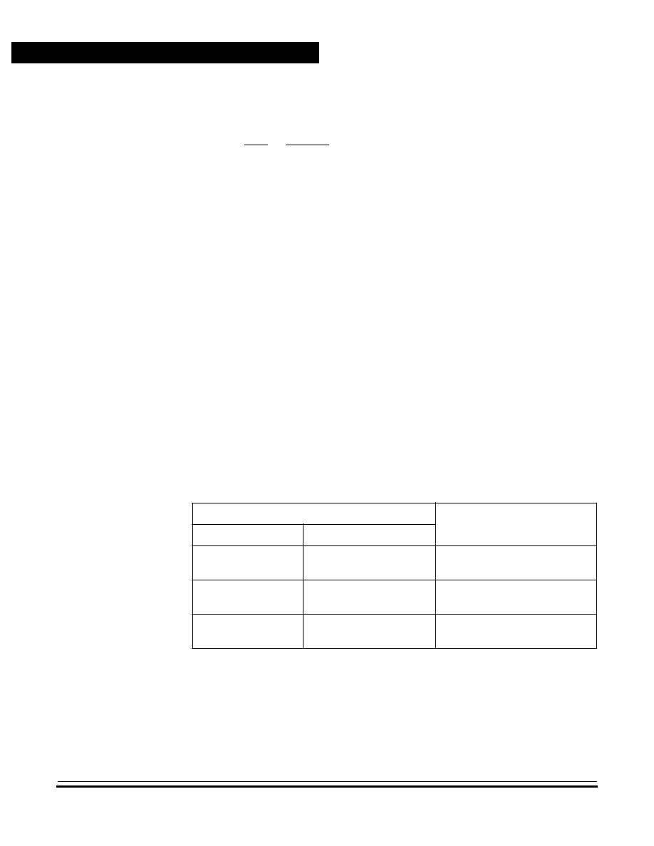
NON-DISCLOSURE AGREEMENT REQUIRED
Operating Modes
Technical Data
MC68HC05P18A
54
Operating Modes
MOTOROLA
If the 16-bit timer interrupt is enabled, it causes the processor to exit wait
mode and resume normal operation. The 16-bit timer may be used to
generate a periodic exit from wait mode. Wait mode may also be exited
when an IRQ or RESET occurs.
NOTE:
If port A interrupts are selected as a mask option, the processor also will
exit wait mode.
6.5 COP Watchdog Timer Considerations
The COP watchdog timer is active in the user mode of operation when
selected by mask option. Executing the STOP instruction without
conversion to halt via mask option causes the COP to be disabled.
Therefore, it is recommended that the STOP instruction be modified to
produce halt mode via mask option if the COP watchdog timer is
enabled.
Furthermore, it is recommended that the COP watchdog timer be
disabled for applications that use the halt or wait mode for time periods
that exceed the COP timeout period.
COP watchdog timer interactions are summarized in
Table 6-1
.
Table 6-1. COP Watchdog Timer Recommendations
IF These Conditions Exist:
THEN the COP Watchdog
Timer Should:
STOP Instruction
WAIT Time
Halt mode selected
via mask option
WAIT time less than
COP timeout
Enable or disable COP
via mask option
Halt mode selected
via mask option
WAIT time MORE than
COP timeout
Disable COP
via mask option
Stop mode selected
via mask option
Any length WAIT time
Disable COP
via mask option

MC68HC05P18A
Technical Data
MOTOROLA
Input/Output (I/O) Ports
55
NON-DISCLOSURE AGREEMENT REQUIRED
Technical Data -- MC68HC05P18A
Section 7. Input/Output (I/O) Ports
7.1 Contents
7.2
Introduction . . . . . . . . . . . . . . . . . . . . . . . . . . . . . . . . . . . . . . . .55
7.3
Port A . . . . . . . . . . . . . . . . . . . . . . . . . . . . . . . . . . . . . . . . . . . .56
7.4
Port B . . . . . . . . . . . . . . . . . . . . . . . . . . . . . . . . . . . . . . . . . . . .57
7.5
Port C . . . . . . . . . . . . . . . . . . . . . . . . . . . . . . . . . . . . . . . . . . . .58
7.6
Port D . . . . . . . . . . . . . . . . . . . . . . . . . . . . . . . . . . . . . . . . . . . .59
7.7
I/O Port Programming. . . . . . . . . . . . . . . . . . . . . . . . . . . . . . . .60
7.2 Introduction
In user mode, 20 bidirectional input/output (I/O) lines are arranged as:
∑
Two 8-bit I/O ports, port A and port C
∑
One 3-bit I/O port, port B
∑
One 1-bit I/O port, port D
These ports are programmable as either inputs or outputs under
software control of the data direction registers (DDRs). There is also an
input-only pin associated with port D.
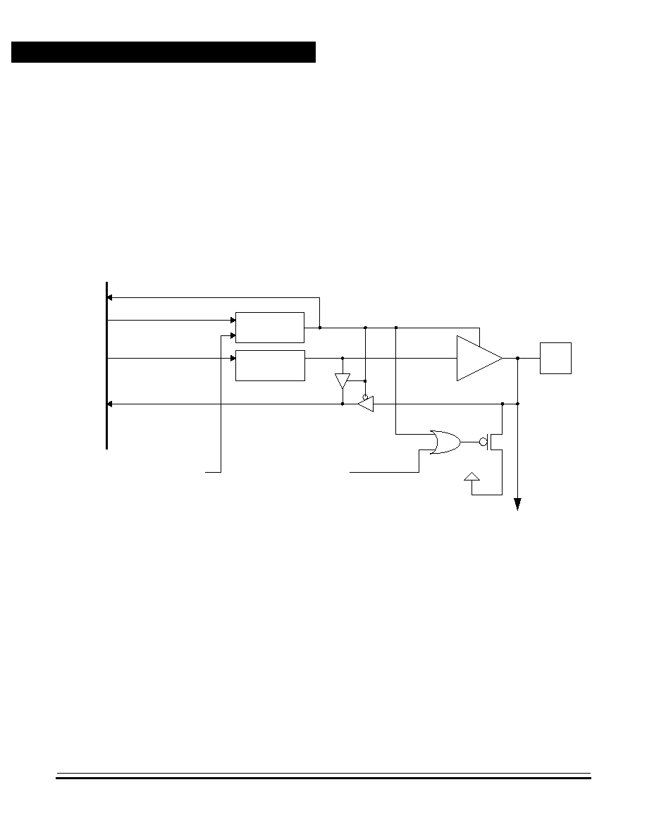
NON-DISCLOSURE AGREEMENT REQUIRED
Input/Output (I/O) Ports
Technical Data
MC68HC05P18A
56
Input/Output (I/O) Ports
MOTOROLA
7.3 Port A
Port A is an 8-bit bidirectional port which can share its pins with the IRQ
interrupt system, as shown in
Figure 7-1
. Each port A pin is controlled
by the corresponding bits in a data direction register and a data register.
The port a data register is located at address $0000. The port A data
direction register (DDRA) is located at address $0004. Reset clears the
DDRA thereby initializing port A as an input port. The port A data register
is unaffected by reset.
Figure 7-1. Port A I/O Circuitry
100
µ
A
PULLUP
READ $0000
WRITE $0000
READ $0004
DATA
REGISTER BIT
TO IRQ
INTERRUPT
SYSTEM
I/O
PIN
OUTPUT
MASK OPTION
(PULLUP INHIBIT)
INTERNAL HC05
DATA BUS
RESET
(RST)
WRITE $0004
DATA DIRECTION
REGISTER BIT
V
DD
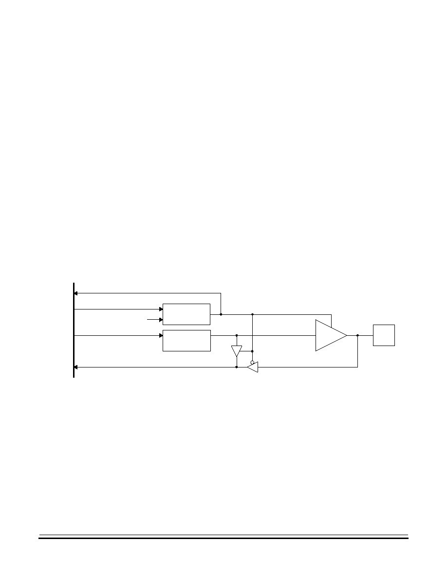
Input/Output (I/O) Ports
Port B
MC68HC05P18A
Technical Data
MOTOROLA
Input/Output (I/O) Ports
57
NON-DISCLOSURE AGREEMENT REQUIRED
7.4 Port B
Port B is a 3-bit bidirectional port that can share pins PB5≠PB7 with the
serial input/output port (SIOP) communications subsystem. The port B
data register is located at address $0001 and its data direction register
(DDR) is located at address $0005. Reset does not affect the data
registers, but clears the DDRs, thereby setting all of the port pins to input
mode. Writing a 1 to a DDR bit sets the corresponding port pin to output
mode (see
Figure 7-2
).
Port B may be used for general I/O applications when the SIOP
subsystem is disabled. The SPE bit in register SIOP control register
(SPCR) is used to enable/disable the SIOP subsystem. When the SIOP
subsystem is enabled, port B registers are still accessible to software.
Writing to either of the port B registers while a data transfer is under way
could corrupt the data. See
Section 9. Serial Input/Output Ports
(SIOP)
for a discussion of the SIOP subsystem.
Figure 7-2. Port B I/O Circuitry
READ $0001
WRITE $0001
READ $0005
DATA
REGISTER BIT
I/O
PIN
OUTPUT
INTERNAL HC05
DATA BUS
RESET
(RST)
WRITE $0005
DATA DIRECTION
REGISTER BIT
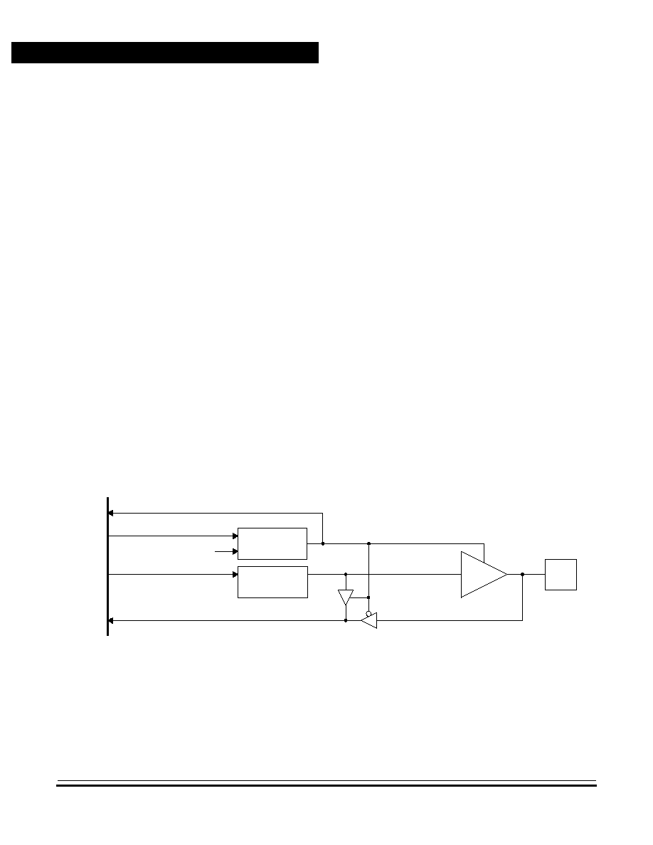
NON-DISCLOSURE AGREEMENT REQUIRED
Input/Output (I/O) Ports
Technical Data
MC68HC05P18A
58
Input/Output (I/O) Ports
MOTOROLA
7.5 Port C
Port C is an 8-bit bidirectional port that can share pins PC3≠PC7 with the
analog-to-digital (A/D) converter subsystem. The port C data register is
located at address $0002 and its data direction register (DDR) is located
at address $0006. Reset does not affect the data registers, but clears the
DDRs, thereby setting all of the port pins to input mode. Writing a 1 to a
DDR bit sets the corresponding port pin to output mode (see
Figure 7-3
). Two port C pins, PC0 and PC1, can source and sink a
higher current than a typical I/O pin. See
Section 13. Electrical
Specifications
regarding current specifications.
Port C may be used for general I/O applications when the A/D
subsystem is disabled. The ADON bit in the A/D status and control
register (ADSC) is used to enable/disable the A/D subsystem.
CAUTION:
Care must be exercised when using pins PC0≠PC2 while the A/D
subsystem is enabled. Accidental changes to bits that affect pins
PC3≠PC7 in the data or DDR registers will produce unpredictable results
in the A/D subsystem.
See
Section 11. Analog-to-Digital (A/D) Converter
.
Figure 7-3. Port C I/O Circuitry
READ $0002
WRITE $0002
READ $0006
DATA
REGISTER BIT
I/O
PIN
OUTPUT
INTERNAL HC05
DATA BUS
RESET
(RST)
WRITE $0006
DATA DIRECTION
REGISTER BIT
HIGH CURRENT
CAPABILITY, PC0
AND PC1 ONLY
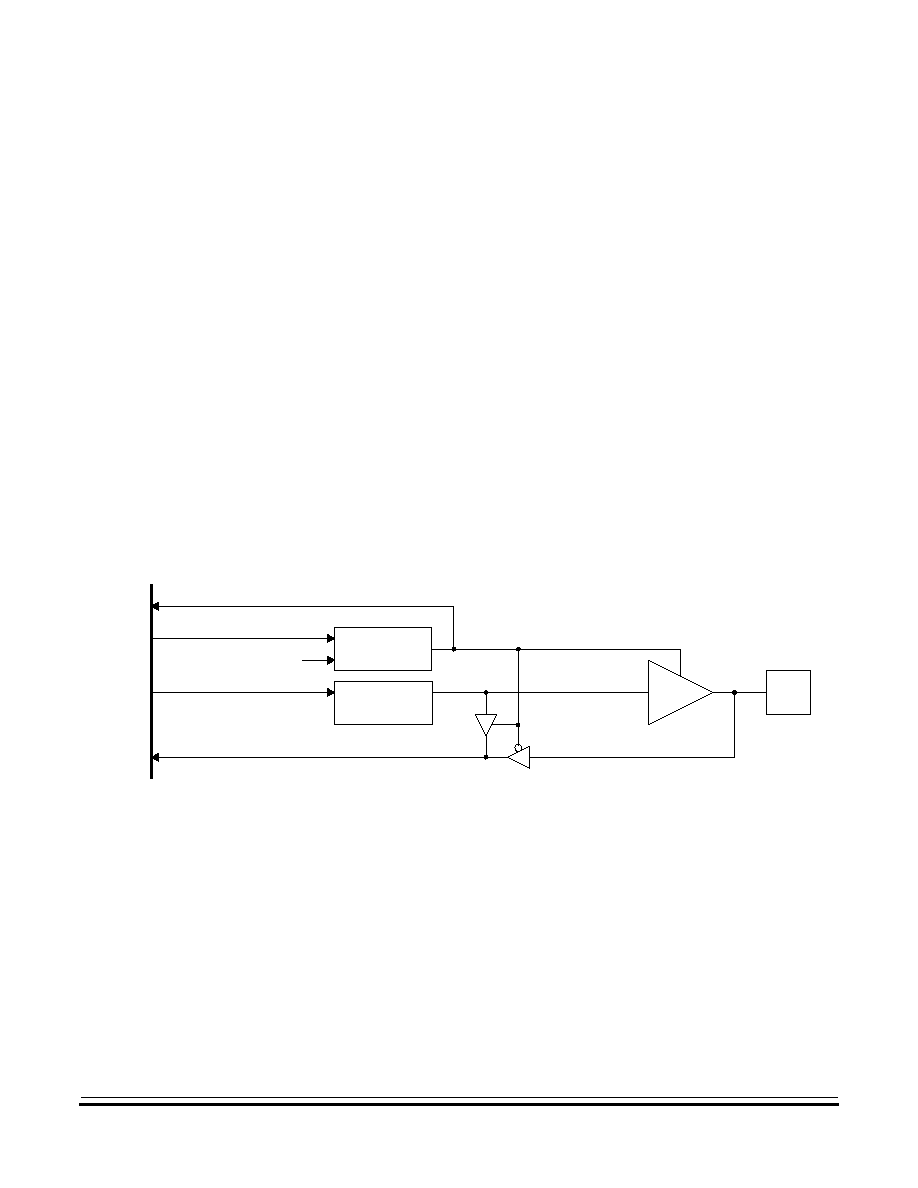
Input/Output (I/O) Ports
Port D
MC68HC05P18A
Technical Data
MOTOROLA
Input/Output (I/O) Ports
59
NON-DISCLOSURE AGREEMENT REQUIRED
7.6 Port D
Port D is a 2-bit port with:
∑
One bidirectional pin, PD5/CKOUT
∑
One input-only pin, PD7
Pin PD7 is shared with the 16-bit timer. There is a mask option to have
PD5 replaced with the clock output. The port D data register is located
at address $0003 and its data direction register (DDR) is located at
address $0007. Reset does not affect the data registers, but clears the
DDRs, thereby setting PD5/CKOUT to input mode. Writing a 1 to DDR
bit 5 sets PD5/CKOUT to output mode (see
Figure 7-4
).
Port D may be used for general I/O applications regardless of the state
of the 16-bit timer. Since PD7 is an input-only line, its state can be read
from the port D data register at any time.
Figure 7-4. Port D I/O Circuitry
READ $0003
WRITE $0003
READ $0007
DATA
REGISTER BIT
I/O
PIN
OUTPUT
INTERNAL HC05
DATA BUS
RESET
(RST)
WRITE $0007
DATA DIRECTION
REGISTER BIT
NON-DISCLOSURE AGREEMENT REQUIRED
Input/Output (I/O) Ports
Technical Data
MC68HC05P18A
60
Input/Output (I/O) Ports
MOTOROLA
7.7 I/O Port Programming
Each pin on ports A through port D, with the exception of pin 7 of port D,
may be programmed as an input or an output under software control as
shown in
Table 7-1
,
Table 7-2
,
Table 7-3
, and
Table 7-4
.
The direction of a pin is determined by the state of its corresponding bit
in the associated port data direction register (DDR). A pin is configured
as an output if its corresponding DDR bit is set to a logic 1. A pin is
configured as an input if its corresponding DDR bit is cleared to a logic 0.
Table 7-1. Port A I/O Pin Functions
DDRA
I/O Pin Mode
Access
to DDRA @ $0004
Access
to Data Register @ $0000
Read/Write
Read
Write
0
In, Hi-Z
DDRA0≠DDRA7
I/O pin
See note
1
Out
DDRA0≠DDRA7
PA0≠PA7
PA0≠PA7
Note: Does not affect input, but stored to data register
Table 7-2. Port B I/O Pin Functions
DDRB
I/O Pin Mode
Access
to DDRB @ $0005
Access
to Data Register @ $0001
Read/Write
Read
Write
0
In, Hi-Z
DDRB5≠DDRB7
I/O pin
See note
1
Out
DDRB5≠DDRB7
PB5≠PB7
PB5≠PB7
Note: Does not affect input, but stored to data register
Table 7-3. Port C I/O Pin Functions
DDRC
I/O Pin Mode
Access
to DDRC @ $0006
Access
to Data Register @ $0002
Read/Write
Read
Write
0
In, Hi-Z
DDRC0≠DDRC7
I/O pin
See note
1
Out
DDRC0≠DDRC7
PC0≠PC7
PC0≠PC7
Note: Does not affect input, but stored to data register
Input/Output (I/O) Ports
I/O Port Programming
MC68HC05P18A
Technical Data
MOTOROLA
Input/Output (I/O) Ports
61
NON-DISCLOSURE AGREEMENT REQUIRED
NOTE:
To avoid generating a glitch on an I/O port pin, data should be written to
the I/O port data register before writing a logical 1 to the corresponding
data direction register.
Table 7-4. Port D I/O Pin Functions
DDRD
I/O Pin Mode
Access
to DDRD @ $0007
Access
to Data Register @ $0003
Read/Write
Read
Write
0
In, Hi-Z
DDRD5
I/O pin
See note
1
Out
DDRD5
PD5/CKOUT
PD5/CKOUT
Note: Does not affect input, but stored to data register
PD7 is input only.

NON-DISCLOSURE AGREEMENT REQUIRED
Input/Output (I/O) Ports
Technical Data
MC68HC05P18A
62
Input/Output (I/O) Ports
MOTOROLA

MC68HC05P18A
Technical Data
MOTOROLA
16-Bit Timer
63
NON-DISCLOSURE AGREEMENT REQUIRED
Technical Data -- MC68HC05P18A
Section 8. 16-Bit Timer
8.1 Contents
8.2
Introduction . . . . . . . . . . . . . . . . . . . . . . . . . . . . . . . . . . . . . . . .63
8.3
Timer. . . . . . . . . . . . . . . . . . . . . . . . . . . . . . . . . . . . . . . . . . . . .65
8.4
Output Compare . . . . . . . . . . . . . . . . . . . . . . . . . . . . . . . . . . . .68
8.5
Input Capture . . . . . . . . . . . . . . . . . . . . . . . . . . . . . . . . . . . . . .70
8.6
Timer Control Register . . . . . . . . . . . . . . . . . . . . . . . . . . . . . . .72
8.7
Timer Status Register . . . . . . . . . . . . . . . . . . . . . . . . . . . . . . . .73
8.8
Timer Operation during Wait Mode and Halt Mode . . . . . . . . .74
8.9
Timer Operating during Stop Mode . . . . . . . . . . . . . . . . . . . . .74
8.2 Introduction
The MC68HC05P18A MCU contains a single 16-bit programmable timer
with an input capture function and an output compare function. The 16-
bit timer is driven by the output of a fixed divide-by-four prescaler
operating from the PH2 clock. The 16-bit timer may be used for many
applications, including input waveform measurement while
simultaneously generating an output waveform. Pulse widths can vary
from microseconds to seconds depending on the oscillator frequency
selected. The 16-bit timer is also capable of generating periodic
interrupts. See
Figure 8-1
.

NON-DISCLOSURE AGREEMENT REQUIRED
16-Bit Timer
Technical Data
MC68HC05P18A
64
16-Bit Timer
MOTOROLA
Figure 8-1. 16-Bit Timer Block Diagram
EDGE
DETECTOR
COMPARE
DETECTOR
OVERFLOW
DETECTOR
PH2
CLOCK
FREE-
RUNNING
COUNTER
INTERNAL HC05 BUS
TIMER
STATUS
REGISTER
OUTPUT
COMPARE
OCRH
OCRL
INPUT
CAPTURE
ICRH
ICRL
OCF
TCAP
˜
4
BUFFER
TMRH/ACRH TMRL/ACRL
TOF
ICF
OCIE
TOIE
ICIE
OLVL
IEDG
TIMER CONTROL
REGISTER
INTERRUPT GENERATOR
R
TCMP
D
>
Q
RESET
TIMER INTERRUPT

16-Bit Timer
Timer
MC68HC05P18A
Technical Data
MOTOROLA
16-Bit Timer
65
NON-DISCLOSURE AGREEMENT REQUIRED
Because the timer has a 16-bit architecture, each function is represented
by two registers. Each register pair contains the high and low byte of that
function. Generally, accessing the low byte of a specific timer function
allows full control of that function; however, an access of the high byte
inhibits that specific timer function until the low byte is also accessed.
NOTE:
The I bit in the condition code register (CCR) should be set while
manipulating both the high and low byte registers of a specific timer
function. This prevents interrupts from occurring between the time that
the high and low bytes are accessed.
8.3 Timer
The key element of the programmable timer is a 16-bit free-running
counter, or timer registers, preceded by a prescaler, which divides the
PH2 clock by four. The prescaler gives the timer a resolution of 2.0 ms
when a 4-MHz crystal is used. The counter is incremented to increasing
values during the low portion of the PH2 clock cycle.
The double byte free-running counter can be read from either of two
locations:
∑
The timer registers, TMRH and TMRL
∑
The alternate counter registers, ACRH and ACRL
Both locations will contain identical values. A read sequence containing
only a read of the least-significant bit (LSB) of the counter (TMRL/ACRL)
returns the count value at the time of the read. If a read of the counter
accesses the most-significant bit (MSB) first (TMRH/ACRH), it causes
the LSB (TMRL/ACRL) to be transferred to a buffer. This buffer value
remains fixed after the first MSB byte read even if the MSB is read
several times. The buffer is accessed when reading the counter LSB
(TMRL/ACRL), and thus completes a read sequence of the total counter
value. When reading either the timer or alternate counter registers, if the
MSB is read, the LSB must also be read to complete the read sequence.
See
Figure 8-2
and
Figure 8-3
.
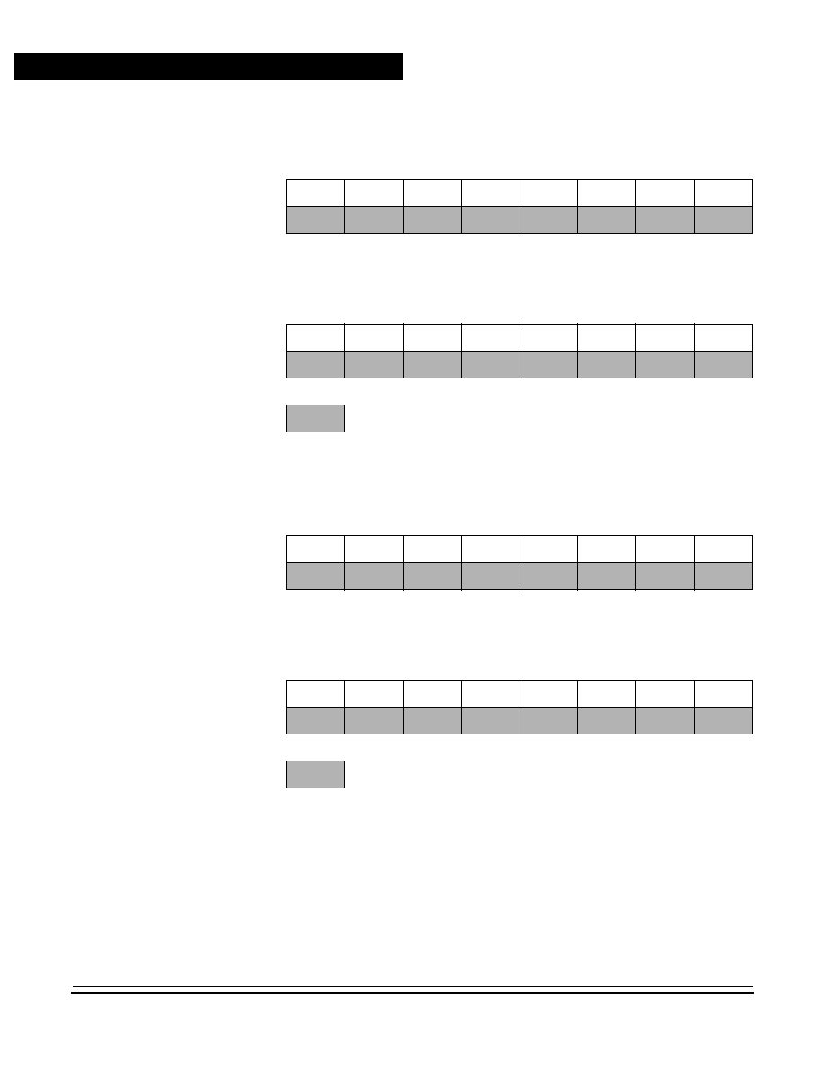
NON-DISCLOSURE AGREEMENT REQUIRED
16-Bit Timer
Technical Data
MC68HC05P18A
66
16-Bit Timer
MOTOROLA
The timer registers and alternate counter registers can be read at any
time without affecting their values. However, the alternate counter
registers differ from the timer registers in one respect: A read of the timer
register MSB can clear the timer overflow flag (TOF). Therefore, the
alternate counter registers can be read at any time without the possibility
Address:
$0018
Bit 7
6
5
4
3
2
1
Bit 0
Read:
TMRH7
TMRH6
TMRH5
TMRH4
TMRH3
TMRH2
TMRH1
TMRH0
Write:
Reset:
1
1
1
1
1
1
1
1
Address:
$0019
Bit 7
6
5
4
3
2
1
Bit 0
Read:
TMRL7
TMRL6
TMRL5
TMRL4
TMRL3
TMRL2
TMRL1
TMRL0
Write:
Reset:
1
1
1
1
1
1
1
1
= Unimplemented
Figure 8-2. Timer Counter Registers (TMRH/TMRL)
Address:
$001A
Bit 7
6
5
4
3
2
1
Bit 0
Read:
ACRH7
ACRH6
ACRH5
ACRH4
ACRH3
ACRH2
ACRH1
ACRH0
Write:
Reset:
1
1
1
1
1
1
1
1
Address:
$001B
Bit 7
6
5
4
3
2
1
Bit 0
Read:
ACRL7
ACRL6
ACRL5
ACRL4
ACRL3
ACRL2
ACRL1
ACRL0
Write:
Reset:
1
1
1
1
1
1
1
1
= Unimplemented
Figure 8-3. Alternate Counter Registers (ACRH/ACRL)
16-Bit Timer
Timer
MC68HC05P18A
Technical Data
MOTOROLA
16-Bit Timer
67
NON-DISCLOSURE AGREEMENT REQUIRED
of missing timer overflow interrupts due to clearing of the TOF. See
Figure 8-4
.
The free-running counter is initialized to $FFFC during reset and is a
read-only register. During power-on reset (POR), the counter is
initialized to $FFFC and begins counting after the oscillator startup
delay. Since the counter is 16 bits preceded by a fixed divide-by-four
prescaler, the value in the counter repeats every 262,144 PH2 clock
cycles (524,288 oscillator cycles). When the free-running counter rolls
over from $FFFF to $0000, the timer overflow flag bit (TOF) in the timer
status register (TSR) is set. An interrupt can also be enabled when
counter rollover occurs by setting the timer overflow interrupt enable bit
(TOIE) in the timer control register (TCR). See
Figure 8-5
.
Figure 8-4. State Timing Diagram for Timer Overflow
Figure 8-5. State Timing Diagram for Timer Reset
$FFFE
$FFFF
$0000
$0001
$0002
16-BIT FREE-RUNNING
COUNTER
TIMER OVERFLOW
FLAG (TOF)
PH2 CLOCK
Note: The TOF bit is set at timer state T11 (transition of counter from $FFFF to $0000). It is cleared by reading the timer
status register (TSR) during the high portion of the PH2 clock followed by reading the LSB of the counter register
pair (TCRL).
Note: The counter and control registers are the only 16-bit timer registers affected by reset.
PH2 CLOCK
INTERNAL RESET
16-BIT FREE-RUNNING
COUNTER
RESET
(EXTERNAL OR OTHER)
$FFFC
$FFFD
$FFFE
$FFFF
NON-DISCLOSURE AGREEMENT REQUIRED
16-Bit Timer
Technical Data
MC68HC05P18A
68
16-Bit Timer
MOTOROLA
8.4 Output Compare
The output compare function may be used to generate an output
waveform and/or as an elapsed time indicator. All of the bits in the output
compare register pair, OCRH/OCRL, are readable and writable and are
not altered by the 16-bit timer's control logic. Reset does not affect the
contents of these registers. If the output compare function is not utilized,
its registers may be used for data storage. See
Figure 8-6
.
The contents of the output compare registers are compared with the
contents of the free-running counter once every four PH2 clock cycles.
If a match is found, the output compare flag bit (OCF) is set and the
output level bit (OLVL) is clocked to the output latch. The values in the
output compare registers and output level bit should be changed after
each successful comparison to control an output waveform or to
establish a new elapsed timeout. An interrupt can also accompany a
successful output compare if the output compare interrupt enable bit
(OCIE) is set.
After a CPU write cycle to the MSB of the output compare register pair
(OCRH), the output compare function is inhibited until the LSB (OCRL)
is written. Both bytes must be written if the MSB is written. A write made
only to the LSB will not inhibit the compare function. The free-running
Address:
$0016
Bit 7
6
5
4
3
2
1
Bit 0
Read:
OCRH7
OCRH6
OCRH5
OCRH4
OCRH3
OCRH2
OCRH1
OCRH0
Write:
Reset:
Unaffected by reset
Address:
$0017
Bit 7
6
5
4
3
2
1
Bit 0
Read:
OCRL7
OCRL6
OCRL5
OCRL4
OCRL3
OCRL2
OCRL1
OCRL0
Write:
Reset:
Unaffected by reset
Figure 8-6. Output Compare Registers (OCRH/OCRL)

16-Bit Timer
Output Compare
MC68HC05P18A
Technical Data
MOTOROLA
16-Bit Timer
69
NON-DISCLOSURE AGREEMENT REQUIRED
counter increments every four PH2 clock cycles. The minimum time
required to update the output compare registers is a function of software
rather than hardware.
The output compare output level bit (OLVL) will be clocked to its output
latch regardless of the state of the output compare flag bit (OCF). A valid
output compare must occur before the OLVL bit is clocked to its output
latch (TCMP).
Since neither the output compare flag (OCF) nor the output compare
registers are affected by reset, care must be exercised when initializing
the output compare function. This procedure is recommended:
1. Block interrupts by setting the I bit in the condition code register
(CCR).
2. Write the MSB of the output compare register pair (OCRH) to
inhibit further compares until the LSB is written.
3. Read the timer status register (TSR) to arm the output compare
flag (OCF).
4. Write the LSB of the output compare register pair (OCRL) to
enable the output compare function and to clear its flag and
interrupt.
5. Unblock interrupts by clearing the I bit in the CCR.
This procedure prevents the output compare flag bit (OCF) from being
set between the time it is read and the time the output compare registers
are updated. A software example is shown in
Figure 8-7
.
9B
∑
∑
B6
BE
B7
B6
BF
∑
∑
∑
XX
XX
16
13
17
∑
SEI
∑
∑
LDA
LDX
STA
LDA
STX
∑
∑
∑
DATAH
DATAL
OCRH
TSR
OCRL
∑
BLOCK INTERRUPTS
∑
∑
HI BYTE FOR COMPARE
LOW BYTE FOR COMPARE
INHIBIT OUTPUT COMPARE
ARM OCF BIT TO CLEAR
READY FOR NEXT COMPARE
∑
Figure 8-7. Output Compare Software Initialization Example
NON-DISCLOSURE AGREEMENT REQUIRED
16-Bit Timer
Technical Data
MC68HC05P18A
70
16-Bit Timer
MOTOROLA
8.5 Input Capture
Two 8-bit read-only registers (ICRH and ICRL) make up the 16-bit input
capture. They are used to latch the value of the free-running counter
after a defined transition is sensed by the input capture edge detector.
NOTE:
The input capture edge detector contains a Schmitt trigger to improve
noise immunity.
The edge that triggers the counter transfer is defined by the input edge
bit (IEDG) in TCR. Reset does not affect the contents of the input
capture registers. See
Figure 8-8
.
The result obtained by an input capture will be one more than the value
of the free-running counter on the rising edge of the PH2 clock preceding
the external transition (see
Figure 8-9
). This delay is required for internal
synchronization. Resolution is affected by the prescaler, allowing the
free-running counter to increment once every four PH2 clock cycles.
The contents of the free-running counter are transferred to the input
capture registers on each proper signal transition regardless of the state
of the input capture flag bit (ICF) in register TSR. The input capture
registers always contain the free-running counter value which
corresponds to the most recent input capture.
Address:
$0014
Bit 7
6
5
4
3
2
1
Bit 0
Read:
ICRH7
ICRH6
ICRH5
ICRH4
ICRH3
ICRH2
ICRH1
ICRH0
Write:
Reset:
Unaffected by reset
Address:
$0015
Bit 7
6
5
4
3
2
1
Bit 0
Read:
ICRL7
ICRL6
ICRL5
ICRL4
ICRL3
ICRL2
ICRL1
ICRL0
Write:
Reset:
Unaffected by reset
Figure 8-8. Input Capture Registers (ICRH/ICRL)
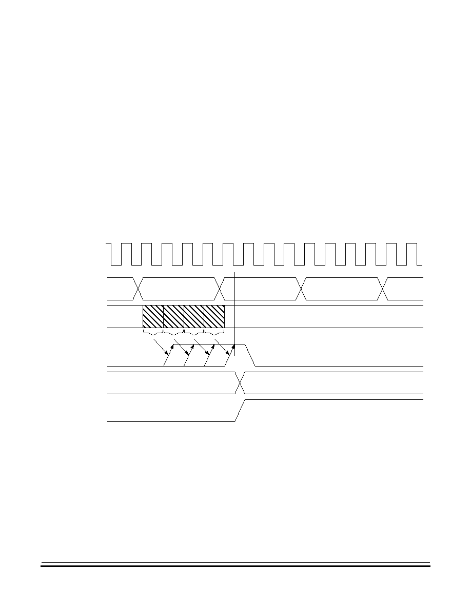
16-Bit Timer
Input Capture
MC68HC05P18A
Technical Data
MOTOROLA
16-Bit Timer
71
NON-DISCLOSURE AGREEMENT REQUIRED
After a read of the MSB of the input capture register pair (ICRH), counter
transfers are inhibited until the LSB of the register pair (ICRL) is also
read. This characteristic forces the minimum pulse period attainable to
be determined by the time required to execute an input capture software
routine in an application.
Reading the LSB of the input capture register pair (ICRL) does not inhibit
transfer of the free-running counter. Again, minimum pulse periods are
ones which allow software to read the LSB of the register pair (ICRL) and
perform needed operations. There is no conflict between reading the
LSB (ICRL) and the free-running counter transfer since they occur on
opposite edges of the PH2 clock.
Figure 8-9. State Timing Diagram for Input Capture
INPUT CAPTURE
FLAG
INPUT CAPTURE
REGISTER
16-BIT FREE-RUNNING
COUNTER
TCAP PIN
INPUT CAPTURE
LATCH
PH2 CLOCK
Note: If the input edge occurs in the shaded area from one T10 timer state to the other T10 timer state, the input capture
flag is set during the next T11 timer state.
$FFEC
$FFED
$FFEE
$FFEF
$FFEB
$FFED
(SEE NOTE)
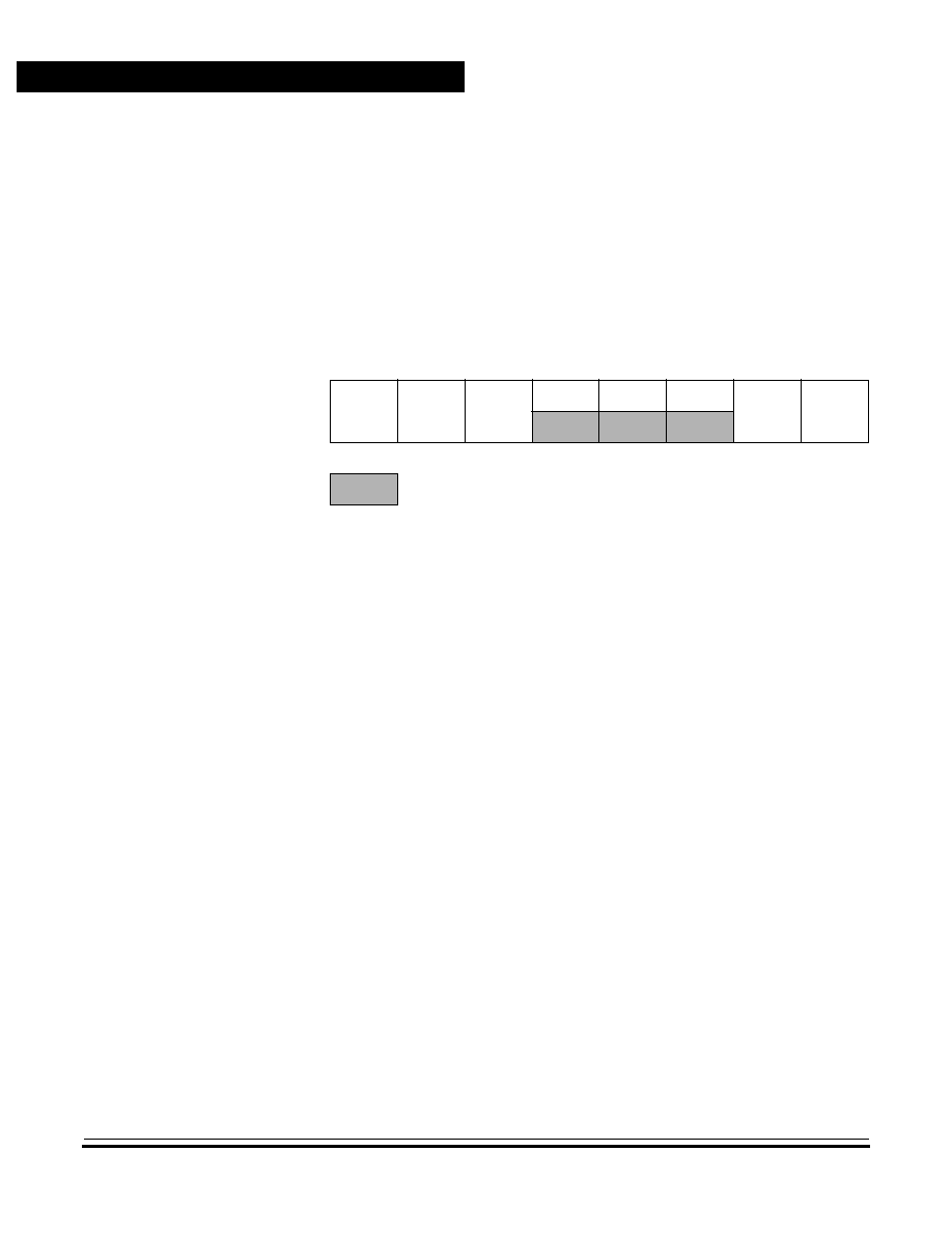
NON-DISCLOSURE AGREEMENT REQUIRED
16-Bit Timer
Technical Data
MC68HC05P18A
72
16-Bit Timer
MOTOROLA
8.6 Timer Control Register
The timer control (TCR) shown in
Figure 8-10
and free-running counter
(TMRH, TMRL, ACRH, ACRL) registers are the only registers of the 16-
bit timer affected by reset. The output compare port (TCMP) is forced
low after reset and remains low until OLVL is set and a valid output
compare occurs.
ICIE -- Input Capture Interrupt Enable Bit
Bit 7, when set, enables input capture interrupts to the CPU. The
interrupt will occur at the same time bit 7 (ICF) in the TSR register is
set.
OCIE -- Output Comapre Interrupt Enable Bit
Bit 6, when set, enables output compare interrupts to the CPU. The
interrupt will occur at the same time bit 6 (OCF) in the TSR register is
set.
TOIE -- Timer Overflow Interrupt Enable Bit
Bit 5, when set, enables timer overflow (rollover) interrupts to the
CPU. The interrupt will occur at the same time bit 5 (TOF) in the TSR
register is set.
IEDG -- Input Capture Edge Select Bit
Bit 1 selects which edge of the input capture signal will trigger a
transfer of the contents of the free-running counter registers to the
input capture registers. Clearing this bit will select the falling edge,
setting it selects the rising edge.
Address:
$0012
Bit 7
6
5
4
3
2
1
Bit 0
Read:
ICIE
OCIE
TOIE
0
0
0
IEDG
OLVL
Write:
Reset:
0
0
0
0
0
0
U
0
= Unimplemented
U = Unaffected
Figure 8-10. Timer Control Register (TCR)

16-Bit Timer
Timer Status Register
MC68HC05P18A
Technical Data
MOTOROLA
16-Bit Timer
73
NON-DISCLOSURE AGREEMENT REQUIRED
OLVL -- Output Compare Output Level Select Bit
Bit 0 selects the output level (high or low) that is clocked into the
output compare output latch at the next successful output compare.
8.7 Timer Status Register
Reading the timer status register (TSR) satisfies the first condition
required to clear status flags and interrupts (see
Figure 8-11
). The only
remaining step is to read (or write) the register associated with the active
status flag (and/or interrupt). This method does not present any
problems for input capture or output compare functions.
However, a problem can occur when using a timer interrupt function and
reading the free-running counter at random times to, for example,
measure an elapsed time. If the proper precautions are not designed into
the application software, a timer interrupt flag (TOF) could
unintentionally be cleared if:
1. The TSR is read when bit 5 (TOF) is set.
2. The LSB of the free-running counter is read, but not for the
purpose of servicing the flag or interrupt.
The alternate counter registers (ACRH and ACRL) contain the same
values as the timer registers (TMRH and TMRL). Registers ACRH and
ACRL can be read at any time without affecting the timer overflow flag
(TOF) or interrupt.
Address:
$0013
Bit 7
6
5
4
3
2
1
Bit 0
Read:
ICF
OCF
TOF
0
0
0
0
0
Write:
Reset:
U
U
U
0
0
0
0
0
= Unimplemented
U = Unaffected
Figure 8-11. Timer Status Register (TSR)

NON-DISCLOSURE AGREEMENT REQUIRED
16-Bit Timer
Technical Data
MC68HC05P18A
74
16-Bit Timer
MOTOROLA
ICF -- Input Capture Flag
Bit 7 is set when the edge specified by IEDG in register TCR has been
sensed by the input capture edge detector fed by pin TCAP. This flag,
and the input capture interrupt, can be cleared by reading register
TSR followed by reading the LSB of the input capture register pair
(ICRL).
OCF -- Output Compare Bit
Bit 6 is set when the contents of the output compare registers match
the contents of the free-running counter. This flag, and the output
compare interrupt, can be cleared by reading register TSR followed
by writing the LSB of the output compare register pair (OCRL).
TOF -- Timer Overflow Flag
Bit 5 is set by a rollover of the free-running counter from $FFFF to
$0000. This flag, and the timer overflow interrupt, can be cleared by
reading register TSR followed by reading the LSB of the timer register
pair (TMRL).
8.8 Timer Operation during Wait Mode and Halt Mode
During wait mode and halt mode the 16-bit timer continues to operate
normally and may generate an interrupt to trigger the MCU out of the wait
mode and halt mode.
8.9 Timer Operating during Stop Mode
When the MCU enters the stop mode, the free-running counter stops
counting. (The PH2 clock is stopped.) It remains at that particular count
value until the stop mode is exited by applying a low signal to the IRQ
pin, at which time the counter resumes from its stopped value as if
nothing had happened. If stop mode is exited via an external RESET
(logic low applied to the RESET pin), the counter is forced to $FFFC.
If a valid input capture edge occurs at the TCAP pin during stop mode,
the input capture detect circuitry is armed. This action does not set any
flags or wake up the MCU, but when the MCU does wake up there will

16-Bit Timer
Timer Operating during Stop Mode
MC68HC05P18A
Technical Data
MOTOROLA
16-Bit Timer
75
NON-DISCLOSURE AGREEMENT REQUIRED
be an active input capture flag (and data) from the first valid edge. If the
stop mode is exited by an external RESET, no input capture flag or data
will be present even if a valid input capture edge was detected during
stop mode.

NON-DISCLOSURE AGREEMENT REQUIRED
16-Bit Timer
Technical Data
MC68HC05P18A
76
16-Bit Timer
MOTOROLA

MC68HC05P18A
Technical Data
MOTOROLA
Serial Input/Output Ports (SIOP)
77
NON-DISCLOSURE AGREEMENT REQUIRED
Technical Data -- MC68HC05P18A
Section 9. Serial Input/Output Ports (SIOP)
9.1 Contents
9.2
Introduction . . . . . . . . . . . . . . . . . . . . . . . . . . . . . . . . . . . . . . . .77
9.3
SIOP Signal Format . . . . . . . . . . . . . . . . . . . . . . . . . . . . . . . . .78
9.3.1
Serial Clock (SCK) . . . . . . . . . . . . . . . . . . . . . . . . . . . . . . . .78
9.3.2
Serial Data Input (SDI) . . . . . . . . . . . . . . . . . . . . . . . . . . . . .79
9.3.3
Serial Data Output (SDO). . . . . . . . . . . . . . . . . . . . . . . . . . .79
9.4
SIOP Registers . . . . . . . . . . . . . . . . . . . . . . . . . . . . . . . . . . . . .80
9.4.1
SIOP Control Register . . . . . . . . . . . . . . . . . . . . . . . . . . . . .80
9.4.2
SIOP Status Register . . . . . . . . . . . . . . . . . . . . . . . . . . . . . .82
9.4.3
SIOP Data Register . . . . . . . . . . . . . . . . . . . . . . . . . . . . . . .83
9.2 Introduction
The simple synchronous serial input/output (I/O) port (SIOP) subsystem
is designed to provide efficient serial communications between
peripheral devices or other MCUs. The SIOP is implemented as a 3-wire
master/slave system with:
∑
Serial clock (SCK)
∑
Serial data input (SDI)
∑
Serial data output (SDO)
A block diagram of the SIOP is shown in
Figure 9-1
.
The SIOP subsystem shares its input/output pins with port B. When the
SIOP is enabled, SPE bit set in the SIOP control register (SCR), port B
data direction register (DDR), and data register are modified by the
SIOP. Although port B DDR and data registers can be altered by
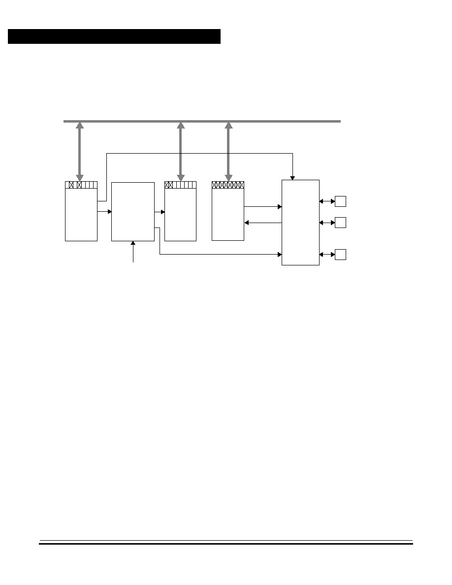
NON-DISCLOSURE AGREEMENT REQUIRED
Serial Input/Output Ports (SIOP)
Technical Data
MC68HC05P18A
78
Serial Input/Output Ports (SIOP)
MOTOROLA
application software, these actions could affect the transmitted or
received data.
Figure 9-1. SIOP Block Diagram
9.3 SIOP Signal Format
The SIOP subsystem is software configurable for master or slave
operation. There are no external mode selection inputs available (for
example, slave select pin).
9.3.1 Serial Clock (SCK)
The state of the SCK output normally remains a logic 1 during idle
periods between data transfers. The first falling edge of SCK signals the
beginning of a data transfer. At this time the first bit of received data is
accepted at the SDI pin and the first bit of transmitted data is presented
at the SDO pin (see
Figure 9-2
). Data is captured at the SDI pin on the
rising edge of SCK, and the first bit of transmitted data is presented at
the SDO pin. The transfer is terminated upon the eighth rising edge of
SCK.
8-BIT
SHIFT
REGISTER
STATUS
REGISTER
BAUD
RATE
CONTROL
REGISTER
GENERATOR
HCO5 INTERNAL BUS
PH2 CLOCK
SCK
SDI
SDO
7 6 5 4 3 2 1 0
7 6 5 4 3 2 1 0
7 6 5 4 3 2 1 0
I/O
$0B
$0C
$0A
CONTROL
LOGIC
SPE
SDI/PB6
SCK/PB7
SDO/PB5
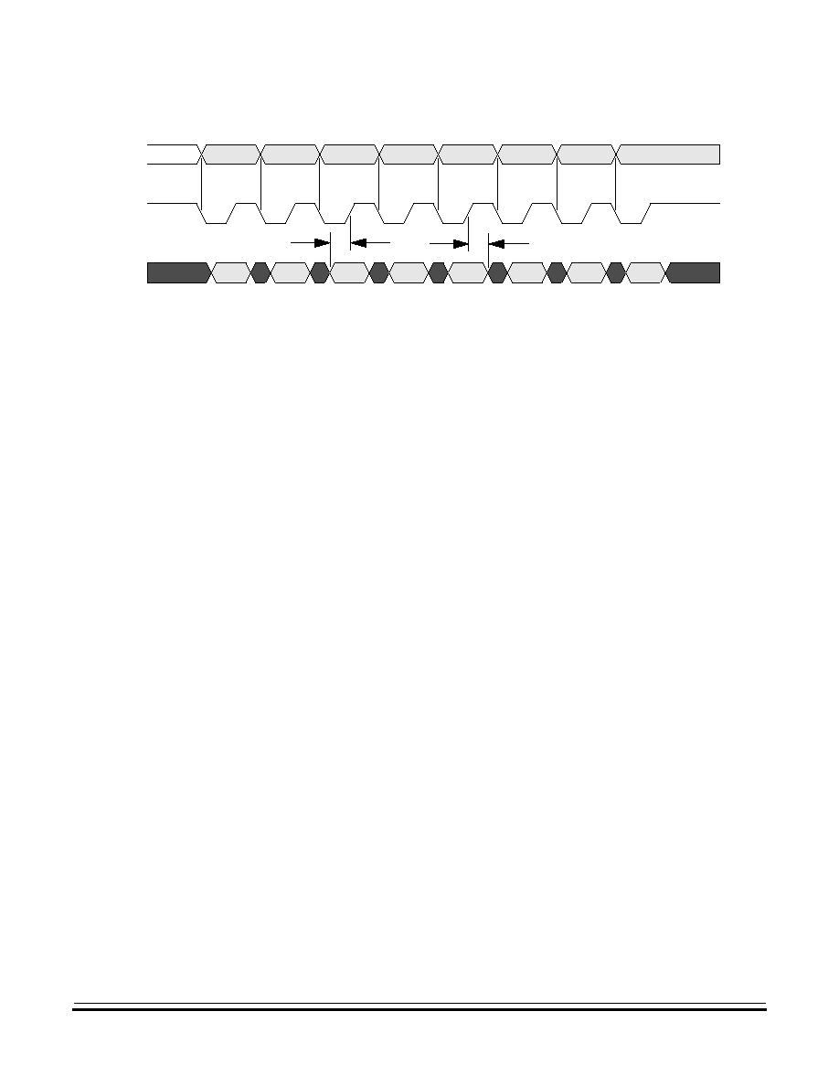
Serial Input/Output Ports (SIOP)
SIOP Signal Format
MC68HC05P18A
Technical Data
MOTOROLA
Serial Input/Output Ports (SIOP)
79
NON-DISCLOSURE AGREEMENT REQUIRED
Figure 9-2. SIOP Timing Diagram
The master and slave modes of operation differ only by the sourcing of
SCK. In master mode, SCK is driven from an internal source within the
MCU. In slave mode, SCK is driven from a source external to the MCU.
The SCK frequency is mask option selectable. Available rates are OSC
divided by 2, 4, 8, or 16.
NOTE:
OSC divided by 2 is four times faster than the standard rate available on
the 68HC05P6.
Refer to
1.4 Mask Options
for a description of available mask options.
9.3.2 Serial Data Input (SDI)
The SDI pin becomes an input as soon as the SIOP subsystem is
enabled. New data is presented to the SDI pin on the falling edge of
SCK. Valid data must be present at least 100 ns before the rising edge
of SCK and remain valid for 100 ns after the rising edge of SCK. See
Figure 9-2
.
9.3.3 Serial Data Output (SDO)
The SDO pin becomes an output as soon as the SIOP subsystem is
enabled. Prior to enabling the SIOP, PB5 can be initialized to determine
the beginning state. While the SIOP is enabled, PB5 cannot be used as
a standard output since that pin is connected to the last stage of the
SIOP serial shift register. A mask option is included to allow the data to
SCK
SDO
SDI
100 ns
100 ns
BIT 0
BIT 1
BIT 2
BIT 3
BIT 4
BIT 5
BIT 6
BIT 7
BIT 0
BIT 1
BIT 2
BIT 3
BIT 4
BIT 5
BIT 6
BIT 7
NON-DISCLOSURE AGREEMENT REQUIRED
Serial Input/Output Ports (SIOP)
Technical Data
MC68HC05P18A
80
Serial Input/Output Ports (SIOP)
MOTOROLA
be transmitted in either most-significant bit (MSB) first format or the
least-significant bit (LSB) format.
On the first falling edge of SCK, the first data bit will be shifted out to the
SDO pin. The remaining data bits will be shifted out to the SDI pin on
subsequent falling edges of SCK. The SDO pin will present valid data at
least 100 ns before the rising edge of the SCK and remain valid for
100 ns after the rising edge of SCK. See
Figure 9-2
.
9.4 SIOP Registers
The SIOP is programmed and controlled by these registers:
∑
SIOP control register (SCR) located at address $000A
∑
SIOP status register (SSR) located at address $000B
∑
SIOP data register (SDR) located at address $000C
9.4.1 SIOP Control Register
This register is located at address $000A and contains two bits.
Figure 9-3
shows the position of each bit in the register and indicates
the value of each bit after reset.
Address:
$000A
Bit 7
6
5
4
3
2
1
Bit 0
Read:
0
SPE
0
MSTR
0
0
0
0
Write:
Reset:
0
0
0
0
0
0
0
0
= Unimplemented
Figure 9-3. SIOP Control Register (SCR)

Serial Input/Output Ports (SIOP)
SIOP Registers
MC68HC05P18A
Technical Data
MOTOROLA
Serial Input/Output Ports (SIOP)
81
NON-DISCLOSURE AGREEMENT REQUIRED
SPE -- Serial Peripheral Enable Bit
When set, the SPE bit enables the SIOP subsystem such that
SDO/PB5 is the serial data output, SDI/PB6 is the serial data input,
and SCK/PB7 is a serial clock input in the slave mode or a serial clock
output in the master mode. The port B DDR and data registers can be
manipulated as usual (except for PB5); however, these actions could
affect the transmitted or received data.
The SPE bit is readable and writable at any time. Clearing the SPE bit
while a transmission is in progress will:
1. Abort the transmission
2. Reset the serial bit counter
3. Convert the port B/SIOP port to a general-purpose I/O port
Reset clears the SPE bit.
MSTR -- Master Mode Select Bit
When set, the MSTR bit configures the serial I/O port for master
mode. A transfer is initiated by writing to the SDR. Also, the SCK pin
becomes an output providing a synchronous data clock dependent
upon the oscillator frequency. When the device is in slave mode, the
SDO and SDI pins do not change function. These pins behave exactly
the same in both the master and slave modes.
The MSTR bit is readable and writable at any time regardless of the
state of the SPE bit. Clearing the MSTR bit will abort any transfers that
may have been in progress. Reset clears the MSTR bit, placing the
SIOP subsystem in slave mode.
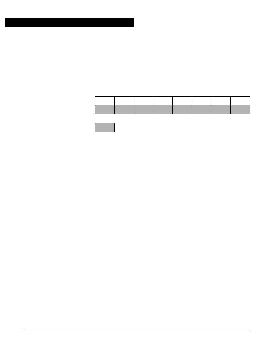
NON-DISCLOSURE AGREEMENT REQUIRED
Serial Input/Output Ports (SIOP)
Technical Data
MC68HC05P18A
82
Serial Input/Output Ports (SIOP)
MOTOROLA
9.4.2 SIOP Status Register
This register is located at address $000B and contains two bits.
Figure 9-4
shows the position of each bit in the register and indicates
the value of each bit after reset.
SPIF -- Serial Port Interface Flag
SPIF is a read-only status bit that is set on the last rising edge of SCK
and indicates that a data transfer has been completed. It has no effect
on any future data transfers and can be ignored. The SPIF bit is
cleared by reading the SSR followed by a read or write of the SDR. If
the SPIF is cleared before the last rising edge of SCK it will be set
again on the last rising edge of SCK. Reset clears the SPIF bit.
DCOL -- Data Collision Bit
DCOL is a read-only status bit, which indicates that an illegal access
of the SDR has occurred. The DCOL bit will be set when reading or
writing the SDR after the first falling edge of SCK and before SPIF is
set. Reading or writing the SDR during this time will result in invalid
data being transmitted or received.
The DCOL bit is cleared by reading the SSR (when the SPIF bit is set)
followed by a read or write of the SDR. If the last part of the clearing
sequence is done after another transfer has started, the DCOL bit will
be set again. Reset clears the DCOL bit.
Address:
$000B
Bit 7
6
5
4
3
2
1
Bit 0
Read:
SPIF
DCOL
0
0
0
0
0
0
Write:
Reset:
0
0
0
0
0
0
0
0
= Unimplemented
Figure 9-4. SIOP Status Register (SSR)

Serial Input/Output Ports (SIOP)
SIOP Registers
MC68HC05P18A
Technical Data
MOTOROLA
Serial Input/Output Ports (SIOP)
83
NON-DISCLOSURE AGREEMENT REQUIRED
9.4.3 SIOP Data Register
This register is located at address $000C and serves as both the
transmit and receive data register. Writing to this register will initiate a
message transmission if the SIOP is in master mode. The SIOP
subsystem is not double buffered and any write to this register will
destroy the previous contents. The SDR can be read at any time;
however, if a transfer is in progress, the results may be ambiguous and
the DCOL bit will be set. Writing to the SDR while a transfer is in
progress can cause invalid data to be transmitted and/or received.
Figure 9-5
shows the position of each bit in the register. This register is
not affected by reset.
Address:
$000C
Bit 7
6
5
4
3
2
1
Bit 0
Read:
SD7
SD6
SD5
SD4
SD3
SD2
SD1
SD0
Write:
Reset:
Unaffected by reset
Figure 9-5. SIOP Data Register (SDR)

NON-DISCLOSURE AGREEMENT REQUIRED
Serial Input/Output Ports (SIOP)
Technical Data
MC68HC05P18A
84
Serial Input/Output Ports (SIOP)
MOTOROLA

MC68HC05P18A
Technical Data
MOTOROLA
EEPROM
85
NON-DISCLOSURE AGREEMENT REQUIRED
Technical Data -- MC68HC05P18A
Section 10. EEPROM
10.1 Contents
10.2
Introduction . . . . . . . . . . . . . . . . . . . . . . . . . . . . . . . . . . . . . . . .85
10.3
EEPROM Programming Register . . . . . . . . . . . . . . . . . . . . . . .86
10.4
Programming/Erasing Procedures . . . . . . . . . . . . . . . . . . . . . .88
10.2 Introduction
The electrically erasable programmable read-only memory (EEPROM)
is located at address $0140 and consists of 128 bytes. Programming the
EEPROM can be done by the user on a single byte basis by
manipulating the programming register, located at address $001C.
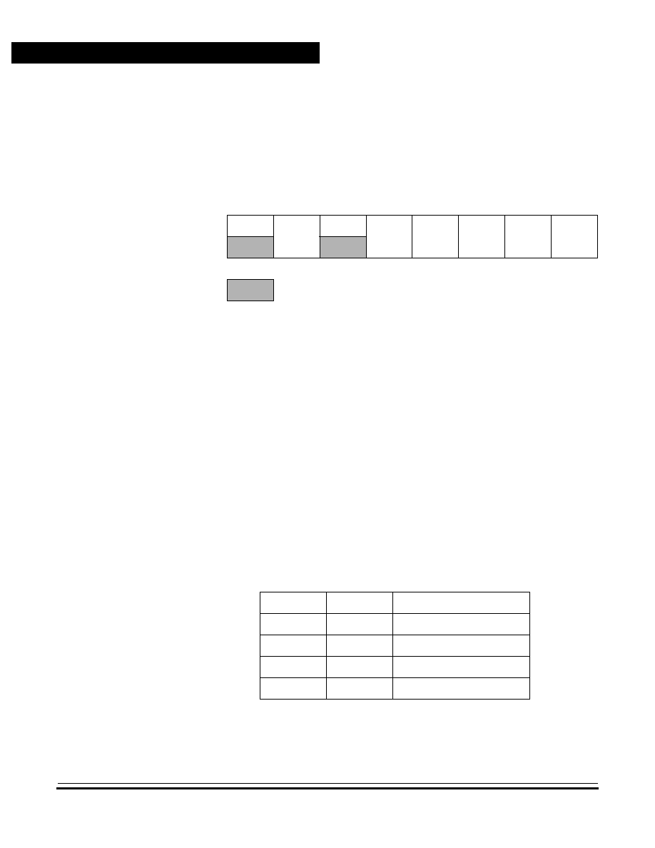
NON-DISCLOSURE AGREEMENT REQUIRED
EEPROM
Technical Data
MC68HC05P18A
86
EEPROM
MOTOROLA
10.3 EEPROM Programming Register
The contents and use of the programming register (EEPROG) are
discussed here.
CPEN -- Charge Pump Enable Bit
When set, CPEN enables the charge pump that produces the internal
EEPROM programming voltage. This bit should be set concurrently
with the LATCH bit. The programming voltage will not be available
until EEPGM is set. The charge pump should be disabled when not in
use. CPEN is readable and writable and is cleared by reset.
ER1 and ER0 -- Erase Select Bits
ER1 and ER0 form a 2-bit field that is used to select one of three
erase modes: byte, block, or bulk.
Table 10-1
shows the modes
selected for each bit configuration. These bits are readable and
writable and are cleared by reset.
Address: $001C
Bit 7
6
5
4
3
2
1
Bit 0
Read:
0
CPEN
0
ER1
ER0
LATCH
EERC
EEPGM
Write:
Reset:
0
0
0
0
0
0
0
0
= Unimplemented
Figure 10-1. EEPROM Programming Register (EEPROG)
Table 10-1. Erase Mode Select
ER1
ER0
Mode
0
0
Program, no erase
0
1
Byte erase
1
0
Block erase
1
1
Bulk erase

EEPROM
EEPROM Programming Register
MC68HC05P18A
Technical Data
MOTOROLA
EEPROM
87
NON-DISCLOSURE AGREEMENT REQUIRED
In byte erase mode, only the selected byte is erased. In block mode,
a 32-byte block of EEPROM is erased. The EEPROM memory space
is divided into four 32-byte blocks ($140≠$15F, $160≠$17F,
$180≠$19F, $1A0≠$1BF), and doing a block erase to any address
within a block erases the entire block. In bulk erase mode, the entire
128-byte EEPROM section is erased.
LATCH -- EEPROM Programming Latch Bit
When set, LATCH configures the EEPROM address and data bus for
programming. When LATCH is set, writes to the EEPROM array
cause the data bus and the address bus to be latched. This bit is
readable and writable, but reads from the array are inhibited if the
LATCH bit is set and a write to the EEPROM space has taken place.
When clear, address and data buses are configured for normal
operation. Reset clears this bit.
EERC -- EEPROM RC Oscillator Control Bit
When this bit is set, the EEPROM section uses the internal RC
oscillator instead of the CPU clock. The RC oscillator is shared with
the analog-to-digital (A/D) converter, so this bit should be set by the
user when the internal bus frequency is below 1.5 MHz to guarantee
reliable operation of the EEPROM or A/D converter. After setting the
EERC bit, delay a time, t
RCON
, to allow the RC oscillator to stabilize.
This bit is readable and writable. The EERC bit is cleared by reset.
The RC oscillator is disabled while the MCU is in stop mode.
EEPGM -- EEPROM Programming Power Enable Bit
EEPGM must be written to enable (or disable) the EEPGM function.
When set, EEPGM turns on the charge pump and enables the
programming (or erasing) power to the EEPROM array. When clear,
this power is switched off. This enables pulsing of the programming
voltage to be controlled internally. This bit can be read at any time, but
can only be written to if LATCH = 1. If LATCH is not set, EEPGM
cannot be set. LATCH and EEPGM cannot both be set with one write
if LATCH is cleared. EEPGM is cleared automatically when LATCH is
cleared. Reset clears this bit.

NON-DISCLOSURE AGREEMENT REQUIRED
EEPROM
Technical Data
MC68HC05P18A
88
EEPROM
MOTOROLA
10.4 Programming/Erasing Procedures
To program a byte of EEPROM:
1. Set EELAT = CPEN = 1.
2. Set ER1 = ER0 = 0.
3. Write data to the desired address.
4. Set EEPGM for a time, t
EEPGM
.
Any bit should be erased before it is programmed. However, if
write/erase cycling is a concern, a procedure can be followed to
minimize the cycling of each bit in each EEPROM byte.
Here is the procedure:
∑
If PB ∑ EB = 0 -- Program the new data over the existing data
without erasing it first.
∑
If PB ∑ EB
0 -- Erase byte before programming.
Where:
PB = Byte data to be programmed
EB = Existing EEPROM byte data
To erase a byte of EEPROM:
1. Set LATCH = 1, CPEN = 1, ER1 = 0, and ER0 = 1.
2. Write to the address to be erased.
3. Set EEPGM for a time, t
EBYT
.
To erase a block of EEPROM:
1. Set LATCH = 1, CPEN = 1, ER1 = 1, and ER0 = 0.
2. Write to any address in the block.
3. Set EEPGM for a time, t
EBLOCK
.

EEPROM
Programming/Erasing Procedures
MC68HC05P18A
Technical Data
MOTOROLA
EEPROM
89
NON-DISCLOSURE AGREEMENT REQUIRED
For a bulk erase:
1. Set LATCH = 1, CPEN = 1, ER1 = 1, and ER0 = 1.
2. Write to any address in the array.
3. Set EEPGM for a time, t
EBULK
.
To terminate the programming or erase sequence, clear EEPGM, delay
for a time, t
FPV
, to allow the programming voltage to fall, and then clear
LATCH and CPEN to free up the buses. Following each erase or
programming sequence, clear all programming control bits.

NON-DISCLOSURE AGREEMENT REQUIRED
EEPROM
Technical Data
MC68HC05P18A
90
EEPROM
MOTOROLA

MC68HC05P18A
Technical Data
MOTOROLA
Analog-to-Digital (A/D) Converter
91
NON-DISCLOSURE AGREEMENT REQUIRED
Technical Data -- MC68HC05P18A
Section 11. Analog-to-Digital (A/D) Converter
11.1 Contents
11.2
Introduction . . . . . . . . . . . . . . . . . . . . . . . . . . . . . . . . . . . . . . . .91
11.3
Analog Section . . . . . . . . . . . . . . . . . . . . . . . . . . . . . . . . . . . . .92
11.3.1
Ratiometric Conversion . . . . . . . . . . . . . . . . . . . . . . . . . . . .92
11.3.2
Reference Supply Voltage (V
REFH
) . . . . . . . . . . . . . . . . . . .92
11.3.3
Accuracy and Precision . . . . . . . . . . . . . . . . . . . . . . . . . . . .92
11.4
Conversion Process . . . . . . . . . . . . . . . . . . . . . . . . . . . . . . . . .92
11.5
Digital Section. . . . . . . . . . . . . . . . . . . . . . . . . . . . . . . . . . . . . .93
11.5.1
Conversion Times . . . . . . . . . . . . . . . . . . . . . . . . . . . . . . . .93
11.5.2
Internal versus External Oscillator . . . . . . . . . . . . . . . . . . . .93
11.5.3
Multi-Channel Operation . . . . . . . . . . . . . . . . . . . . . . . . . . .94
11.6
A/D Status and Control Register. . . . . . . . . . . . . . . . . . . . . . . .94
11.7
A/D Conversion Data Register . . . . . . . . . . . . . . . . . . . . . . . . .96
11.8
A/D Subsystem Operation during Wait Mode
and Halt Mode . . . . . . . . . . . . . . . . . . . . . . . . . . . . . . . . . . .96
11.9
A/D Subsystem Operation during Stop Mode. . . . . . . . . . . . . .96
11.2 Introduction
The MC68HC05P18A includes a 4-channel, multiplexed input, 8-bit,
successive approximation analog-to-digital (A/D) converter. The A/D
subsystem shares its inputs with port C pins PC3≠PC7.

NON-DISCLOSURE AGREEMENT REQUIRED
Analog-to-Digital (A/D) Converter
Technical Data
MC68HC05P18A
92
Analog-to-Digital (A/D) Converter
MOTOROLA
11.3 Analog Section
The following paragraphs describe the operation and performance of
analog modules within the analog subsystem.
11.3.1 Ratiometric Conversion
The A/D converter is ratiometric, with pin V
REFH
supplying the high
reference voltage. Applying an input voltage equal to V
REFH
produces a
conversion result of $FF (full scale). Applying an input voltage equal to
V
SS
produces a conversion result of $00. An input voltage greater than
V
REFH
converts to $FF with no overflow indication. For ratiometric
conversions, V
REFH
should be at the same potential as the supply
voltage being used by the analog signal being measured and be
referenced to V
SS
.
11.3.2 Reference Supply Voltage (V
REFH
)
The reference supply for the A/D converter shares pin PC7 with port C.
The low reference is tied to the V
SS
pin internally. V
REFH
can be any
voltage between V
SS
and V
DD
; however, the accuracy of conversions is
tested and guaranteed only for V
REFH
= V
DD
.
11.3.3 Accuracy and Precision
The 8-bit conversion result is accurate to within
±
1 1/2 LSB (least
significant bit), including quantization; however, the accuracy of
conversions is tested and guaranteed only with external oscillator
operation.
11.4 Conversion Process
The A/D reference inputs are applied to a precision digital-to-analog
(D/A) converter. Control logic drives the D/A and the analog output is
successively compared to the selected analog input that was sampled at

Analog-to-Digital (A/D) Converter
Digital Section
MC68HC05P18A
Technical Data
MOTOROLA
Analog-to-Digital (A/D) Converter
93
NON-DISCLOSURE AGREEMENT REQUIRED
the beginning of the conversion cycle. The conversion process is
monotonic and has no missing codes.
11.5 Digital Section
The following paragraphs describe the operation and performance of
digital modules within the analog subsystem.
11.5.1 Conversion Times
Each input conversion requires 32 PH2 clock cycles, which must be at a
frequency equal to or greater than 1 MHz.
11.5.2 Internal versus External Oscillator
If the MCU PH2 clock frequency is less than 1 MHz (2 MHz external
oscillator), the internal RC oscillator (approximately 1.5 MHz) must be
used for the A/D converter clock. The internal RC clock is selected by
setting the EERC bit in the EEPROM program register (EEPROG).
NOTE:
The RC oscillator is shared with the EEPROM module. The RC oscillator
is disabled while the MCU is in stop mode.
When the internal RC oscillator is being used, these limitations apply:
1. Since the internal RC oscillator is running asynchronously with
respect to the PH2 clock, the conversion complete (CC) bit in the
A/D status and control register (ADSC) must be used to determine
when a conversion sequence has been completed.
2. Electrical noise slightly degrades the accuracy of the A/D
converter. The A/D converter is synchronized to read voltages
during the quiet period of the clock driving it. Since the internal and
external clocks are not synchronized, the A/D converter
occasionally measures an input when the external clock is making
a transition.
3. If the PH2 clock is 1 MHz or greater (for example, external
oscillator 2 MHz or greater), the internal RC oscillator should be
turned off and the external oscillator used as the conversion clock.
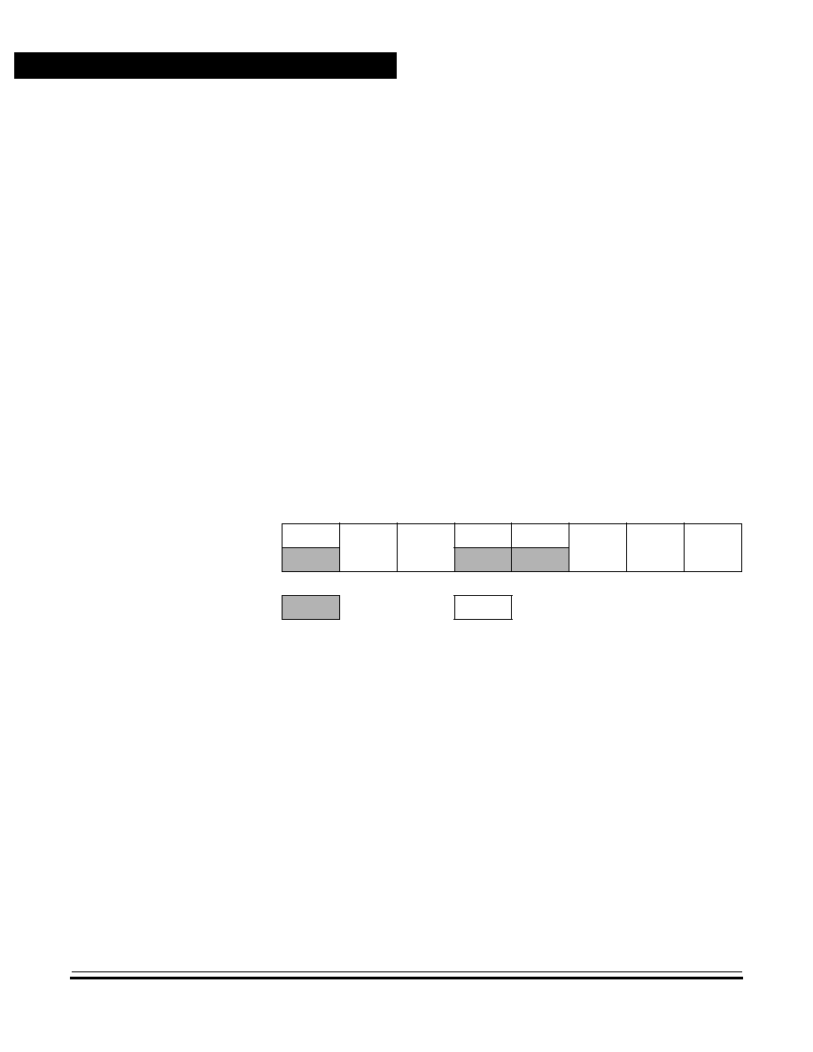
NON-DISCLOSURE AGREEMENT REQUIRED
Analog-to-Digital (A/D) Converter
Technical Data
MC68HC05P18A
94
Analog-to-Digital (A/D) Converter
MOTOROLA
11.5.3 Multi-Channel Operation
An input multiplexer allows the A/D converter to select from one of four
external analog signals. Port C pins PC3≠PC6 are shared with the inputs
to the multiplexer.
11.6 A/D Status and Control Register
The A/D status and control register (ADSCR) reports the completion of
A/D conversion and provides control over:
∑
Oscillator selection
∑
Analog subsystem power
∑
Input channel selection
See
Figure 11-1
.
CC -- Conversion Complete Bit
This read-only status bit is set when a conversion sequence has
completed and data is ready to be read from the ADC register. CC is
cleared when a channel is selected for conversion, when data is read
from the ADC register, or when the A/D subsystem is turned off. Once
a conversion is started, conversions of the selected channel continue
every 32 PH2 clock cycles until the ADSC register is written to again.
During continuous conversion operation, the ADC register is updated
with new data, and the CC bit is set, every 32 PH2 clock cycles. Also,
data from the previous conversion is overwritten regardless of the
state of the CC bit.
Address:
$001E
Bit 7
6
5
4
3
2
1
Bit 0
Read:
CC
R
ADON
0
0
CH2
CH1
CH0
Write:
Reset:
0
0
0
0
0
0
0
0
= Unimplemented
R
= Reserved
Figure 11-1. A/D Status and Control Register (ADSCR)

Analog-to-Digital (A/D) Converter
A/D Status and Control Register
MC68HC05P18A
Technical Data
MOTOROLA
Analog-to-Digital (A/D) Converter
95
NON-DISCLOSURE AGREEMENT REQUIRED
R -- Reserved Bit
This bit is not currently used. It can be read or written, but does not
control anything.
ADON -- A/D Subsystem On Bit
When the A/D subsystem is turned on (ADON = 1), it requires a time
t
ADON
to stabilize before accurate conversion results can be attained.
CH2≠CH0 -- Channel Select Bits
CH2, CH1, and CH0 form a 3-bit field that is used to select an input to
the A/D converter. Channels 0≠3 correspond to port C input pins
PC6≠PC3. Channels 4≠6 are used for reference measurements. In
user mode, channel 7 is reserved. If a conversion is attempted with
channel 7 selected, the result is $00.
Table 11-1
lists the inputs
selected by bits CH0≠CH3.
If the ADON bit is set, and an input from channels 0≠4 is selected, the
corresponding port C pin's DDR bit is cleared (making that port C pin
an input). If the port C data register is read while the A/D is on, and
one of the shared input channels is selected using bit CH0≠CH2, the
corresponding port C pin reads as a logic 0. The remaining port C pins
read normally. To digitally read a port C pin, the A/D subsystem must
be disabled (ADON = 0) or input channel 5≠7 must be selected.
Table 11-1. A/D Multiplexer Input
Channel Assignments
Channel
Signal
0
AD0 port C bit 6
1
AD1 port C bit 5
2
AD2 port C bit 4
3
AD3 port C bit 3
4
V
REFH
port C bit 7
5
(V
REFH
+ V
SS
)/2
6
V
SS
7
Reserved
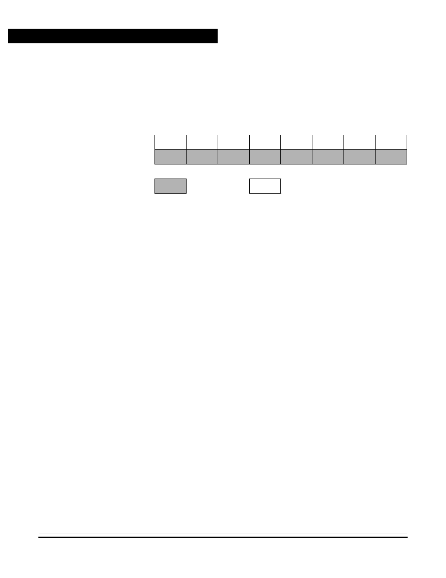
NON-DISCLOSURE AGREEMENT REQUIRED
Analog-to-Digital (A/D) Converter
Technical Data
MC68HC05P18A
96
Analog-to-Digital (A/D) Converter
MOTOROLA
11.7 A/D Conversion Value Data Register
This register contains the output of the A/D converter. See
Figure 11-2
.
11.8 A/D Subsystem Operation during Wait Mode and Halt Mode
The A/D subsystem continues normal operation during wait mode and
halt mode. To decrease power consumption during wait or halt, the
ADON bit in the ADSC register and the EERC bit in the EEPROG
register should be cleared if the A/D subsystem is not being used.
11.9 A/D Subsystem Operation during Stop Mode
When stop mode is enabled, execution of the STOP instruction
terminates all A/D subsystem functions. Any pending conversion is
aborted. When the oscillator resumes operation upon leaving the stop
mode, a finite amount of time passes before the A/D subsystem
stabilizes sufficiently to provide conversions at its rated accuracy. The
delays built into the MC68HC05P18A when coming out of stop mode are
sufficient for this purpose. No explicit delays need to be added to the
application software.
Address:
$001D
Bit 7
6
5
4
3
2
1
Bit 0
Read:
AD7
AD6
AD5
AD4
AD3
AD2
AD1
AD0
Write:
Reset:
Unaffected by reset
= Unimplemented
R
= Reserved
Figure 11-2. A/D Conversion Value Data Register (ADC)

MC68HC05P18A
Technical Data
MOTOROLA
Instruction Set
97
NON-DISCLOSURE AGREEMENT REQUIRED
Technical Data -- MC68HC05P18A
Section 12. Instruction Set
12.1 Contents
12.2
Introduction . . . . . . . . . . . . . . . . . . . . . . . . . . . . . . . . . . . . . . . .98
12.3
Addressing Modes . . . . . . . . . . . . . . . . . . . . . . . . . . . . . . . . . .98
12.3.1
Inherent . . . . . . . . . . . . . . . . . . . . . . . . . . . . . . . . . . . . . . . .99
12.3.2
Immediate. . . . . . . . . . . . . . . . . . . . . . . . . . . . . . . . . . . . . . .99
12.3.3
Direct . . . . . . . . . . . . . . . . . . . . . . . . . . . . . . . . . . . . . . . . . .99
12.3.4
Extended . . . . . . . . . . . . . . . . . . . . . . . . . . . . . . . . . . . . . . .99
12.3.5
Indexed, No Offset . . . . . . . . . . . . . . . . . . . . . . . . . . . . . . .100
12.3.6
Indexed, 8-Bit Offset. . . . . . . . . . . . . . . . . . . . . . . . . . . . . .100
12.3.7
Indexed,16-Bit Offset . . . . . . . . . . . . . . . . . . . . . . . . . . . . .100
12.3.8
Relative . . . . . . . . . . . . . . . . . . . . . . . . . . . . . . . . . . . . . . .101
12.4
Instruction Types . . . . . . . . . . . . . . . . . . . . . . . . . . . . . . . . . .101
12.4.1
Register/Memory Instructions. . . . . . . . . . . . . . . . . . . . . . .102
12.4.2
Read-Modify-Write Instructions . . . . . . . . . . . . . . . . . . . . .103
12.4.3
Jump/Branch Instructions . . . . . . . . . . . . . . . . . . . . . . . . . .104
12.4.4
Bit Manipulation Instructions . . . . . . . . . . . . . . . . . . . . . . .106
12.4.5
Control Instructions . . . . . . . . . . . . . . . . . . . . . . . . . . . . . .107
12.5
Instruction Set Summary . . . . . . . . . . . . . . . . . . . . . . . . . . . .108

NON-DISCLOSURE AGREEMENT REQUIRED
Instruction Set
Technical Data
MC68HC05P18A
98
Instruction Set
MOTOROLA
12.2 Introduction
The MCU instruction set has 62 instructions and uses eight addressing
modes. The instructions include all those of the M146805 CMOS Family
plus one more: the unsigned multiply (MUL) instruction. The MUL
instruction allows unsigned multiplication of the contents of the
accumulator (A) and the index register (X). The high-order product is
stored in the index register, and the low-order product is stored in the
accumulator.
12.3 Addressing Modes
The CPU uses eight addressing modes for flexibility in accessing data.
The addressing modes provide eight different ways for the CPU to find
the data required to execute an instruction.
The eight addressing modes are:
∑
Inherent
∑
Immediate
∑
Direct
∑
Extended
∑
Indexed, no offset
∑
Indexed, 8-bit offset
∑
Indexed, 16-bit offset
∑
Relative

Instruction Set
Addressing Modes
MC68HC05P18A
Technical Data
MOTOROLA
Instruction Set
99
NON-DISCLOSURE AGREEMENT REQUIRED
12.3.1 Inherent
Inherent instructions are those that have no operand, such as return
from interrupt (RTI) and stop (STOP). Some of the inherent instructions
act on data in the CPU registers, such as set carry flag (SEC) and
increment accumulator (INCA). Inherent instructions require no operand
address and are one byte long.
12.3.2 Immediate
Immediate instructions are those that contain a value to be used in an
operation with the value in the accumulator or index register. Immediate
instructions require no operand address and are two bytes long. The
opcode is the first byte, and the immediate data value is the second byte.
12.3.3 Direct
Direct instructions can access any of the first 256 memory locations with
two bytes. The first byte is the opcode, and the second is the low byte of
the operand address. In direct addressing, the CPU automatically uses
$00 as the high byte of the operand address.
12.3.4 Extended
Extended instructions use three bytes and can access any address in
memory. The first byte is the opcode; the second and third bytes are the
high and low bytes of the operand address.
When using the Motorola assembler, the programmer does not need to
specify whether an instruction is direct or extended. The assembler
automatically selects the shortest form of the instruction.

NON-DISCLOSURE AGREEMENT REQUIRED
Instruction Set
Technical Data
MC68HC05P18A
100
Instruction Set
MOTOROLA
12.3.5 Indexed, No Offset
Indexed instructions with no offset are 1-byte instructions that can
access data with variable addresses within the first 256 memory
locations. The index register contains the low byte of the effective
address of the operand. The CPU automatically uses $00 as the high
byte, so these instructions can address locations $0000≠$00FF.
Indexed, no offset instructions are often used to move a pointer through
a table or to hold the address of a frequently used RAM or I/O location.
12.3.6 Indexed, 8-Bit Offset
Indexed, 8-bit offset instructions are 2-byte instructions that can access
data with variable addresses within the first 511 memory locations. The
CPU adds the unsigned byte in the index register to the unsigned byte
following the opcode. The sum is the effective address of the operand.
These instructions can access locations $0000≠$01FE.
Indexed 8-bit offset instructions are useful for selecting the kth element
in an n-element table. The table can begin anywhere within the first 256
memory locations and could extend as far as location 510 ($01FE). The
k value is typically in the index register, and the address of the beginning
of the table is in the byte following the opcode.
12.3.7 Indexed,16-Bit Offset
Indexed, 16-bit offset instructions are 3-byte instructions that can access
data with variable addresses at any location in memory. The CPU adds
the unsigned byte in the index register to the two unsigned bytes
following the opcode. The sum is the effective address of the operand.
The first byte after the opcode is the high byte of the 16-bit offset; the
second byte is the low byte of the offset.
Indexed, 16-bit offset instructions are useful for selecting the kth element
in an n-element table anywhere in memory.
As with direct and extended addressing, the Motorola assembler
determines the shortest form of indexed addressing.

Instruction Set
Instruction Types
MC68HC05P18A
Technical Data
MOTOROLA
Instruction Set
101
NON-DISCLOSURE AGREEMENT REQUIRED
12.3.8 Relative
Relative addressing is only for branch instructions. If the branch
condition is true, the CPU finds the effective branch destination by
adding the signed byte following the opcode to the contents of the
program counter. If the branch condition is not true, the CPU goes to the
next instruction. The offset is a signed, two's complement byte that gives
a branching range of ≠128 to +127 bytes from the address of the next
location after the branch instruction.
When using the Motorola assembler, the programmer does not need to
calculate the offset, because the assembler determines the proper offset
and verifies that it is within the span of the branch.
12.4 Instruction Types
The MCU instructions fall into five categories:
∑
Register/memory instructions
∑
Read-modify-write instructions
∑
Jump/branch instructions
∑
Bit manipulation instructions
∑
Control instructions
NON-DISCLOSURE AGREEMENT REQUIRED
Instruction Set
Technical Data
MC68HC05P18A
102
Instruction Set
MOTOROLA
12.4.1 Register/Memory Instructions
These instructions operate on CPU registers and memory locations.
Most of them use two operands. One operand is in either the
accumulator or the index register. The CPU finds the other operand in
memory.
Table 12-1. Register/Memory Instructions
Instruction
Mnemonic
Add memory byte and carry bit to accumulator
ADC
Add memory byte to accumulator
ADD
AND memory byte with accumulator
AND
Bit test accumulator
BIT
Compare accumulator
CMP
Compare index register with memory byte
CPX
Exclusive OR accumulator with memory byte
EOR
Load accumulator with memory byte
LDA
Load Index register with memory byte
LDX
Multiply
MUL
OR accumulator with memory byte
ORA
Subtract memory byte and carry bit from
accumulator
SBC
Store accumulator in memory
STA
Store index register in memory
STX
Subtract memory byte from accumulator
SUB
Instruction Set
Instruction Types
MC68HC05P18A
Technical Data
MOTOROLA
Instruction Set
103
NON-DISCLOSURE AGREEMENT REQUIRED
12.4.2 Read-Modify-Write Instructions
These instructions read a memory location or a register, modify its
contents, and write the modified value back to the memory location or to
the register.
NOTE:
Do not use read-modify-write operations on write-only registers.
Table 12-2. Read-Modify-Write Instructions
Instruction
Mnemonic
Arithmetic shift left (same as LSL)
ASL
Arithmetic shift right
ASR
Bit clear
BCLR
(1)
1. Unlike other read-modify-write instructions, BCLR and BSET use
only direct addressing.
Bit set
BSET
(1)
Clear register
CLR
Complement (one's complement)
COM
Decrement
DEC
Increment
INC
Logical shift left (same as ASL)
LSL
Logical shift right
LSR
Negate (two's complement)
NEG
Rotate left through carry bit
ROL
Rotate right through carry bit
ROR
Test for negative or zero
TST
(2)
2. TST is an exception to the read-modify-write sequence because it
does not write a replacement value.

NON-DISCLOSURE AGREEMENT REQUIRED
Instruction Set
Technical Data
MC68HC05P18A
104
Instruction Set
MOTOROLA
12.4.3 Jump/Branch Instructions
Jump instructions allow the CPU to interrupt the normal sequence of the
program counter. The unconditional jump instruction (JMP) and the
jump-to-subroutine instruction (JSR) have no register operand. Branch
instructions allow the CPU to interrupt the normal sequence of the
program counter when a test condition is met. If the test condition is not
met, the branch is not performed.
The BRCLR and BRSET instructions cause a branch based on the state
of any readable bit in the first 256 memory locations. These 3-byte
instructions use a combination of direct addressing and relative
addressing. The direct address of the byte to be tested is in the byte
following the opcode. The third byte is the signed offset byte. The CPU
finds the effective branch destination by adding the third byte to the
program counter if the specified bit tests true. The bit to be tested and its
condition (set or clear) is part of the opcode. The span of branching is
from ≠128 to +127 from the address of the next location after the branch
instruction. The CPU also transfers the tested bit to the carry/borrow bit
of the condition code register.
Instruction Set
Instruction Types
MC68HC05P18A
Technical Data
MOTOROLA
Instruction Set
105
NON-DISCLOSURE AGREEMENT REQUIRED
Table 12-3. Jump and Branch Instructions
Instruction
Mnemonic
Branch if carry bit clear
BCC
Branch if carry bit set
BCS
Branch if equal
BEQ
Branch if half-carry bit clear
BHCC
Branch if half-carry bit set
BHCS
Branch if higher
BHI
Branch if higher or same
BHS
Branch if IRQ pin high
BIH
Branch if IRQ pin low
BIL
Branch if lower
BLO
Branch if lower or same
BLS
Branch if interrupt mask clear
BMC
Branch if minus
BMI
Branch if interrupt mask set
BMS
Branch if not equal
BNE
Branch if plus
BPL
Branch always
BRA
Branch if bit clear
BRCLR
Branch never
BRN
Branch if bit set
BRSET
Branch to subroutine
BSR
Unconditional jump
JMP
Jump to subroutine
JSR

NON-DISCLOSURE AGREEMENT REQUIRED
Instruction Set
Technical Data
MC68HC05P18A
106
Instruction Set
MOTOROLA
12.4.4 Bit Manipulation Instructions
The CPU can set or clear any writable bit in the first 256 bytes of
memory, which includes I/O registers and on-chip RAM locations. The
CPU can also test and branch based on the state of any bit in any of the
first 256 memory locations.
Table 12-4. Bit Manipulation Instructions
Instruction
Mnemonic
Bit clear
BCLR
Branch if bit clear
BRCLR
Branch if bit set
BRSET
Bit set
BSET
Instruction Set
Instruction Types
MC68HC05P18A
Technical Data
MOTOROLA
Instruction Set
107
NON-DISCLOSURE AGREEMENT REQUIRED
12.4.5 Control Instructions
These instructions act on CPU registers and control CPU operation
during program execution.
Table 12-5. Control Instructions
Instruction
Mnemonic
Clear carry bit
CLC
Clear interrupt mask
CLI
No operation
NOP
Reset stack pointer
RSP
Return from interrupt
RTI
Return from subroutine
RTS
Set carry bit
SEC
Set interrupt mask
SEI
Stop oscillator and enable IRQ pin
STOP
Software interrupt
SWI
Transfer accumulator to index register
TAX
Transfer index register to accumulator
TXA
Stop CPU clock and enable interrupts
WAIT

NON-DISCLOSURE AGREEMENT REQUIRED
Instruction Set
Technical Data
MC68HC05P18A
108
Instruction Set
MOTOROLA
12.5 Instruction Set Summary
Table 12-6. Instruction Set Summary (Sheet 1 of 6)
Source
Form
Operation
Description
Effect on
CCR
Address
Mode
Opcode
Operand
Cycles
H I N Z C
ADC #opr
ADC opr
ADC opr
ADC opr,X
ADC opr,X
ADC ,X
Add with Carry
A
(A) + (M) + (C)
--
IMM
DIR
EXT
IX2
IX1
IX
A9
B9
C9
D9
E9
F9
ii
dd
hh ll
ee ff
ff
2
3
4
5
4
3
ADD #opr
ADD opr
ADD opr
ADD opr,X
ADD opr,X
ADD ,X
Add without Carry
A
(A) + (M)
--
IMM
DIR
EXT
IX2
IX1
IX
AB
BB
CB
DB
EB
FB
ii
dd
hh ll
ee ff
ff
2
3
4
5
4
3
AND #opr
AND opr
AND opr
AND opr,X
AND opr,X
AND ,X
Logical AND
A
(A)
(M)
-- --
--
IMM
DIR
EXT
IX2
IX1
IX
A4
B4
C4
D4
E4
F4
ii
dd
hh ll
ee ff
ff
2
3
4
5
4
3
ASL opr
ASLA
ASLX
ASL opr,X
ASL ,X
Arithmetic Shift Left (Same as LSL)
-- --
DIR
INH
INH
IX1
IX
38
48
58
68
78
dd
ff
5
3
3
6
5
ASR opr
ASRA
ASRX
ASR opr,X
ASR ,X
Arithmetic Shift Right
-- --
DIR
INH
INH
IX1
IX
37
47
57
67
77
dd
ff
5
3
3
6
5
BCC rel
Branch if Carry Bit Clear
PC
(PC) + 2 + rel ? C = 0
-- -- -- -- --
REL
24
rr
3
BCLR n opr
Clear Bit n
Mn
0
-- -- -- -- --
DIR (b0)
DIR (b1)
DIR (b2)
DIR (b3)
DIR (b4)
DIR (b5)
DIR (b6)
DIR (b7)
11
13
15
17
19
1B
1D
1F
dd
dd
dd
dd
dd
dd
dd
dd
5
5
5
5
5
5
5
5
BCS rel
Branch if Carry Bit Set (Same as BLO)
PC
(PC) + 2 + rel ? C = 1
-- -- -- -- --
REL
25
rr
3
BEQ rel
Branch if Equal
PC
(PC) + 2 + rel ? Z = 1
-- -- -- -- --
REL
27
rr
3
BHCC rel
Branch if Half-Carry Bit Clear
PC
(PC) + 2 + rel ? H = 0
-- -- -- -- --
REL
28
rr
3
BHCS rel
Branch if Half-Carry Bit Set
PC
(PC) + 2 + rel ? H = 1
-- -- -- -- --
REL
29
rr
3
BHI rel
Branch if Higher
PC
(PC) + 2 + rel ? C
Z = 0 -- -- -- -- --
REL
22
rr
3
BHS rel
Branch if Higher or Same
PC
(PC) + 2 + rel ? C = 0
-- -- -- -- --
REL
24
rr
3
C
b0
b7
0
b0
b7
C
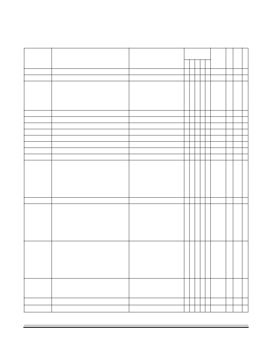
Instruction Set
Instruction Set Summary
MC68HC05P18A
Technical Data
MOTOROLA
Instruction Set
109
NON-DISCLOSURE AGREEMENT REQUIRED
BIH rel
Branch if IRQ Pin High
PC
(PC) + 2 + rel ? IRQ = 1
-- -- -- -- --
REL
2F
rr
3
BIL rel
Branch if IRQ Pin Low
PC
(PC) + 2 + rel ? IRQ = 0
-- -- -- -- --
REL
2E
rr
3
BIT #opr
BIT opr
BIT opr
BIT opr,X
BIT opr,X
BIT ,X
Bit Test Accumulator with Memory Byte
(A)
(M)
-- --
--
IMM
DIR
EXT
IX2
IX1
IX
A5
B5
C5
D5
E5
F5
ii
dd
hh ll
ee ff
ff
2
3
4
5
4
3
BLO rel
Branch if Lower (Same as BCS)
PC
(PC) + 2 + rel ? C = 1
-- -- -- -- --
REL
25
rr
3
BLS rel
Branch if Lower or Same
PC
(PC) + 2 + rel ? C
Z = 1 -- -- -- -- --
REL
23
rr
3
BMC rel
Branch if Interrupt Mask Clear
PC
(PC) + 2 + rel ? I = 0
-- -- -- -- --
REL
2C
rr
3
BMI rel
Branch if Minus
PC
(PC) + 2 + rel ? N = 1
-- -- -- -- --
REL
2B
rr
3
BMS rel
Branch if Interrupt Mask Set
PC
(PC) + 2 + rel ? I = 1
-- -- -- -- --
REL
2D
rr
3
BNE rel
Branch if Not Equal
PC
(PC) + 2 + rel ? Z = 0
-- -- -- -- --
REL
26
rr
3
BPL rel
Branch if Plus
PC
(PC) + 2 + rel ? N = 0
-- -- -- -- --
REL
2A
rr
3
BRA rel
Branch Always
PC
(PC) + 2 + rel ? 1 = 1
-- -- -- -- --
REL
20
rr
3
BRCLR n opr rel Branch if Bit n Clear
PC
(PC) + 2 + rel ? Mn = 0
-- -- -- --
DIR (b0)
DIR (b1)
DIR (b2)
DIR (b3)
DIR (b4)
DIR (b5)
DIR (b6)
DIR (b7)
01
03
05
07
09
0B
0D
0F
dd rr
dd rr
dd rr
dd rr
dd rr
dd rr
dd rr
dd rr
5
5
5
5
5
5
5
5
BRN rel
Branch Never
PC
(PC) + 2 + rel ? 1 = 0
-- -- -- -- --
REL
21
rr
3
BRSET n opr rel Branch if Bit n Set
PC
(PC) + 2 + rel ? Mn = 1
-- -- -- --
DIR (b0)
DIR (b1)
DIR (b2)
DIR (b3)
DIR (b4)
DIR (b5)
DIR (b6)
DIR (b7)
00
02
04
06
08
0A
0C
0E
dd rr
dd rr
dd rr
dd rr
dd rr
dd rr
dd rr
dd rr
5
5
5
5
5
5
5
5
BSET n opr
Set Bit n
Mn
1
-- -- -- -- --
DIR (b0)
DIR (b1)
DIR (b2)
DIR (b3)
DIR (b4)
DIR (b5)
DIR (b6)
DIR (b7)
10
12
14
16
18
1A
1C
1E
dd
dd
dd
dd
dd
dd
dd
dd
5
5
5
5
5
5
5
5
BSR rel
Branch to Subroutine
PC
(PC) + 2; push (PCL)
SP
(SP) ≠ 1; push (PCH)
SP
(SP) ≠ 1
PC
(PC) + rel
-- -- -- -- --
REL
AD
rr
6
CLC
Clear Carry Bit
C
0
-- -- -- -- 0
INH
98
2
CLI
Clear Interrupt Mask
I
0
-- 0 -- -- --
INH
9A
2
Table 12-6. Instruction Set Summary (Sheet 2 of 6)
Source
Form
Operation
Description
Effect on
CCR
Address
Mode
Opcode
Operand
Cycles
H I N Z C

NON-DISCLOSURE AGREEMENT REQUIRED
Instruction Set
Technical Data
MC68HC05P18A
110
Instruction Set
MOTOROLA
CLR opr
CLRA
CLRX
CLR opr,X
CLR ,X
Clear Byte
M
$00
A
$00
X
$00
M
$00
M
$00
-- -- 0
1 --
DIR
INH
INH
IX1
IX
3F
4F
5F
6F
7F
dd
ff
5
3
3
6
5
CMP #opr
CMP opr
CMP opr
CMP opr,X
CMP opr,X
CMP ,X
Compare Accumulator with Memory Byte
(A) ≠ (M)
-- --
IMM
DIR
EXT
IX2
IX1
IX
A1
B1
C1
D1
E1
F1
ii
dd
hh ll
ee ff
ff
2
3
4
5
4
3
COM opr
COMA
COMX
COM opr,X
COM ,X
Complement Byte (One's Complement)
M
(M) = $FF ≠ (M)
A
(A) = $FF ≠ (A)
X
(X) = $FF ≠ (X)
M
(M) = $FF ≠ (M)
M
(M) = $FF ≠ (M)
-- --
1
DIR
INH
INH
IX1
IX
33
43
53
63
73
dd
ff
5
3
3
6
5
CPX #opr
CPX opr
CPX opr
CPX opr,X
CPX opr,X
CPX ,X
Compare Index Register with Memory Byte
(X) ≠ (M)
-- --
IMM
DIR
EXT
IX2
IX1
IX
A3
B3
C3
D3
E3
F3
ii
dd
hh ll
ee ff
ff
2
3
4
5
4
3
DEC opr
DECA
DECX
DEC opr,X
DEC ,X
Decrement Byte
M
(M) ≠ 1
A
(A) ≠ 1
X
(X) ≠ 1
M
(M) ≠ 1
M
(M) ≠ 1
-- --
--
DIR
INH
INH
IX1
IX
3A
4A
5A
6A
7A
dd
ff
5
3
3
6
5
EOR #opr
EOR opr
EOR opr
EOR opr,X
EOR opr,X
EOR ,X
EXCLUSIVE OR Accumulator with Memory
Byte
A
(A)
(M)
-- --
--
IMM
DIR
EXT
IX2
IX1
IX
A8
B8
C8
D8
E8
F8
ii
dd
hh ll
ee ff
ff
2
3
4
5
4
3
INC opr
INCA
INCX
INC opr,X
INC ,X
Increment Byte
M
(M) + 1
A
(A) + 1
X
(X) + 1
M
(M) + 1
M
(M) + 1
-- --
--
DIR
INH
INH
IX1
IX
3C
4C
5C
6C
7C
dd
ff
5
3
3
6
5
JMP opr
JMP opr
JMP opr,X
JMP opr,X
JMP ,X
Unconditional Jump
PC
Jump Address
-- -- -- -- --
DIR
EXT
IX2
IX1
IX
BC
CC
DC
EC
FC
dd
hh ll
ee ff
ff
2
3
4
3
2
Table 12-6. Instruction Set Summary (Sheet 3 of 6)
Source
Form
Operation
Description
Effect on
CCR
Address
Mode
Opcode
Operand
Cycles
H I N Z C

Instruction Set
Instruction Set Summary
MC68HC05P18A
Technical Data
MOTOROLA
Instruction Set
111
NON-DISCLOSURE AGREEMENT REQUIRED
JSR opr
JSR opr
JSR opr,X
JSR opr,X
JSR ,X
Jump to Subroutine
PC
(PC) + n (n = 1, 2, or 3)
Push (PCL); SP
(SP) ≠ 1
Push (PCH); SP
(SP) ≠ 1
PC
Effective Address
-- -- -- -- --
DIR
EXT
IX2
IX1
IX
BD
CD
DD
ED
FD
dd
hh ll
ee ff
ff
5
6
7
6
5
LDA #opr
LDA opr
LDA opr
LDA opr,X
LDA opr,X
LDA ,X
Load Accumulator with Memory Byte
A
(M)
-- --
--
IMM
DIR
EXT
IX2
IX1
IX
A6
B6
C6
D6
E6
F6
ii
dd
hh ll
ee ff
ff
2
3
4
5
4
3
LDX #opr
LDX opr
LDX opr
LDX opr,X
LDX opr,X
LDX ,X
Load Index Register with Memory Byte
X
(M)
-- --
--
IMM
DIR
EXT
IX2
IX1
IX
AE
BE
CE
DE
EE
FE
ii
dd
hh ll
ee ff
ff
2
3
4
5
4
3
LSL opr
LSLA
LSLX
LSL opr,X
LSL ,X
Logical Shift Left (Same as ASL)
-- --
DIR
INH
INH
IX1
IX
38
48
58
68
78
dd
ff
5
3
3
6
5
LSR opr
LSRA
LSRX
LSR opr,X
LSR ,X
Logical Shift Right
-- -- 0
DIR
INH
INH
IX1
IX
34
44
54
64
74
dd
ff
5
3
3
6
5
MUL
Unsigned Multiply
X : A
(X)
◊
(A)
0 -- -- -- 0
INH
42
1
1
NEG opr
NEGA
NEGX
NEG opr,X
NEG ,X
Negate Byte (Two's Complement)
M
≠(M) = $00 ≠ (M)
A
≠(A) = $00 ≠ (A)
X
≠(X) = $00 ≠ (X)
M
≠(M) = $00 ≠ (M)
M
≠(M) = $00 ≠ (M)
-- --
DIR
INH
INH
IX1
IX
30
40
50
60
70
dd
ff
5
3
3
6
5
NOP
No Operation
-- -- -- -- --
INH
9D
2
ORA #opr
ORA opr
ORA opr
ORA opr,X
ORA opr,X
ORA ,X
Logical OR Accumulator with Memory
A
(A)
(M)
-- --
--
IMM
DIR
EXT
IX2
IX1
IX
AA
BA
CA
DA
EA
FA
ii
dd
hh ll
ee ff
ff
2
3
4
5
4
3
ROL opr
ROLA
ROLX
ROL opr,X
ROL ,X
Rotate Byte Left through Carry Bit
-- --
DIR
INH
INH
IX1
IX
39
49
59
69
79
dd
ff
5
3
3
6
5
Table 12-6. Instruction Set Summary (Sheet 4 of 6)
Source
Form
Operation
Description
Effect on
CCR
Address
Mode
Opcode
Operand
Cycles
H I N Z C
C
b0
b7
0
b0
b7
C
0
C
b0
b7
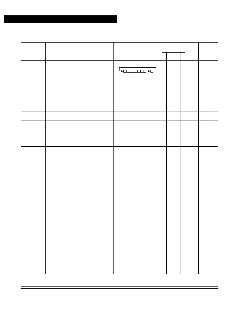
NON-DISCLOSURE AGREEMENT REQUIRED
Instruction Set
Technical Data
MC68HC05P18A
112
Instruction Set
MOTOROLA
ROR opr
RORA
RORX
ROR opr,X
ROR ,X
Rotate Byte Right through Carry Bit
-- --
DIR
INH
INH
IX1
IX
36
46
56
66
76
dd
ff
5
3
3
6
5
RSP
Reset Stack Pointer
SP
$00FF
-- -- -- -- --
INH
9C
2
RTI
Return from Interrupt
SP
(SP) + 1; Pull (CCR)
SP
(SP) + 1; Pull (A)
SP
(SP) + 1; Pull (X)
SP
(SP) + 1; Pull (PCH)
SP
(SP) + 1; Pull (PCL)
INH
80
9
RTS
Return from Subroutine
SP
(SP) + 1; Pull (PCH)
SP
(SP) + 1; Pull (PCL)
-- -- -- -- --
INH
81
6
SBC #opr
SBC opr
SBC opr
SBC opr,X
SBC opr,X
SBC ,X
Subtract Memory Byte and Carry Bit from
Accumulator
A
(A) ≠ (M) ≠ (C)
-- --
IMM
DIR
EXT
IX2
IX1
IX
A2
B2
C2
D2
E2
F2
ii
dd
hh ll
ee ff
ff
2
3
4
5
4
3
SEC
Set Carry Bit
C
1
-- -- -- -- 1
INH
99
2
SEI
Set Interrupt Mask
I
1
-- 1 -- -- --
INH
9B
2
STA opr
STA opr
STA opr,X
STA opr,X
STA ,X
Store Accumulator in Memory
M
(A)
-- --
--
DIR
EXT
IX2
IX1
IX
B7
C7
D7
E7
F7
dd
hh ll
ee ff
ff
4
5
6
5
4
STOP
Stop Oscillator and Enable IRQ Pin
-- 0 -- -- --
INH
8E
2
STX opr
STX opr
STX opr,X
STX opr,X
STX ,X
Store Index Register In Memory
M
(X)
-- --
--
DIR
EXT
IX2
IX1
IX
BF
CF
DF
EF
FF
dd
hh ll
ee ff
ff
4
5
6
5
4
SUB #opr
SUB opr
SUB opr
SUB opr,X
SUB opr,X
SUB ,X
Subtract Memory Byte from Accumulator
A
(A) ≠ (M)
-- --
IMM
DIR
EXT
IX2
IX1
IX
A0
B0
C0
D0
E0
F0
ii
dd
hh ll
ee ff
ff
2
3
4
5
4
3
SWI
Software Interrupt
PC
(PC) + 1; Push (PCL)
SP
(SP) ≠ 1; Push (PCH)
SP
(SP) ≠ 1; Push (X)
SP
(SP) ≠ 1; Push (A)
SP
(SP) ≠ 1; Push (CCR)
SP
(SP) ≠ 1; I
1
PCH
Interrupt Vector High Byte
PCL
Interrupt Vector Low Byte
-- 1 -- -- --
INH
83
1
0
TAX
Transfer Accumulator to Index Register
X
(A)
-- -- -- -- --
INH
97
2
Table 12-6. Instruction Set Summary (Sheet 5 of 6)
Source
Form
Operation
Description
Effect on
CCR
Address
Mode
Opcode
Operand
Cycles
H I N Z C
b0
b7
C

Instruction Set
Instruction Set Summary
MC68HC05P18A
Technical Data
MOTOROLA
Instruction Set
113
NON-DISCLOSURE AGREEMENT REQUIRED
TST opr
TSTA
TSTX
TST opr,X
TST ,X
Test Memory Byte for Negative or Zero
(M) ≠ $00
-- --
--
DIR
INH
INH
IX1
IX
3D
4D
5D
6D
7D
dd
ff
4
3
3
5
4
TXA
Transfer Index Register to Accumulator
A
(X)
-- -- -- -- --
INH
9F
2
WAIT
Stop CPU Clock and Enable Interrupts
-- 0 -- -- --
INH
8F
2
A
Accumulator
opr
Operand (one or two bytes)
C
Carry/borrow flag
PC
Program counter
CCR
Condition code register
PCH
Program counter high byte
dd
Direct address of operand
PCL
Program counter low byte
dd rr
Direct address of operand and relative offset of branch instruction
REL
Relative addressing mode
DIR
Direct addressing mode
rel
Relative program counter offset byte
ee ff
High and low bytes of offset in indexed, 16-bit offset addressing
rr
Relative program counter offset byte
EXT
Extended addressing mode
SP
Stack pointer
ff
Offset byte in indexed, 8-bit offset addressing
X
Index register
H
Half-carry flag
Z
Zero flag
hh ll
High and low bytes of operand address in extended addressing
#
Immediate value
I
Interrupt mask
Logical AND
ii
Immediate operand byte
Logical OR
IMM
Immediate addressing mode
Logical EXCLUSIVE OR
INH
Inherent addressing mode
( )
Contents of
IX
Indexed, no offset addressing mode
≠( )
Negation (two's complement)
IX1
Indexed, 8-bit offset addressing mode
Loaded with
IX2
Indexed, 16-bit offset addressing mode
?
If
M
Memory location
:
Concatenated with
N
Negative flag
Set or cleared
n
Any bit
--
Not affected
Table 12-6. Instruction Set Summary (Sheet 6 of 6)
Source
Form
Operation
Description
Effect on
CCR
Address
Mode
Opcode
Operand
Cycles
H I N Z C

N O N - D I S C L O S U R E A G R E E M E N T R E Q U I R E D
Technical Data
MC68HC05P18A
114
Instruction Set
MOTOROLA
Instr
uction Set
Table 12-7. Opcode Map
Bit Manipulation
Branch
Read-Modify-Write
Control
Register/Memory
DIR
DIR
REL
DIR
INH
INH
IX1
IX
INH
INH
IMM
DIR
EXT
IX2
IX1
IX
0
1
2
3
4
5
6
7
8
9
A
B
C
D
E
F
0
5
BRSET0
3
DIR
5
BSET0
2
DIR
3
BRA
2
REL
5
NEG
2
DIR
3
NEGA
1
INH
3
NEGX
1
INH
6
NEG
2
IX1
5
NEG
1
IX
9
RTI
1
INH
2
SUB
2
IMM
3
SUB
2
DIR
4
SUB
3
EXT
5
SUB
3
IX2
4
SUB
2
IX1
3
SUB
1
IX
0
1
5
BRCLR0
3
DIR
5
BCLR0
2
DIR
3
BRN
2
REL
6
RTS
1
INH
2
CMP
2
IMM
3
CMP
2
DIR
4
CMP
3
EXT
5
CMP
3
IX2
4
CMP
2
IX1
3
CMP
1
IX
1
2
5
BRSET1
3
DIR
5
BSET1
2
DIR
3
BHI
2
REL
11
MUL
1
INH
2
SBC
2
IMM
3
SBC
2
DIR
4
SBC
3
EXT
5
SBC
3
IX2
4
SBC
2
IX1
3
SBC
1
IX
2
3
5
BRCLR1
3
DIR
5
BCLR1
2
DIR
3
BLS
2
REL
5
COM
2
DIR
3
COMA
1
INH
3
COMX
1
INH
6
COM
2
IX1
5
COM
1
IX
10
SWI
1
INH
2
CPX
2
IMM
3
CPX
2
DIR
4
CPX
3
EXT
5
CPX
3
IX2
4
CPX
2
IX1
3
CPX
1
IX
3
4
5
BRSET2
3
DIR
5
BSET2
2
DIR
3
BCC
2
REL
5
LSR
2
DIR
3
LSRA
1
INH
3
LSRX
1
INH
6
LSR
2
IX1
5
LSR
1
IX
2
AND
2
IMM
3
AND
2
DIR
4
AND
3
EXT
5
AND
3
IX2
4
AND
2
IX1
3
AND
1
IX
4
5
5
BRCLR2
3
DIR
5
BCLR2
2
DIR
3
BCS/BLO
2
REL
2
BIT
2
IMM
3
BIT
2
DIR
4
BIT
3
EXT
5
BIT
3
IX2
4
BIT
2
IX1
3
BIT
1
IX
5
6
5
BRSET3
3
DIR
5
BSET3
2
DIR
3
BNE
2
REL
5
ROR
2
DIR
3
RORA
1
INH
3
RORX
1
INH
6
ROR
2
IX1
5
ROR
1
IX
2
LDA
2
IMM
3
LDA
2
DIR
4
LDA
3
EXT
5
LDA
3
IX2
4
LDA
2
IX1
3
LDA
1
IX
6
7
5
BRCLR3
3
DIR
5
BCLR3
2
DIR
3
BEQ
2
REL
5
ASR
2
DIR
3
ASRA
1
INH
3
ASRX
1
INH
6
ASR
2
IX1
5
ASR
1
IX
2
TAX
1
INH
4
STA
2
DIR
5
STA
3
EXT
6
STA
3
IX2
5
STA
2
IX1
4
STA
1
IX
7
8
5
BRSET4
3
DIR
5
BSET4
2
DIR
3
BHCC
2
REL
5
ASL/LSL
2
DIR
3
ASLA/LSLA
1
INH
3
ASLX/LSLX
1
INH
6
ASL/LSL
2
IX1
5
ASL/LSL
1
IX
2
CLC
1
INH
2
EOR
2
IMM
3
EOR
2
DIR
4
EOR
3
EXT
5
EOR
3
IX2
4
EOR
2
IX1
3
EOR
1
IX
8
9
5
BRCLR4
3
DIR
5
BCLR4
2
DIR
3
BHCS
2
REL
5
ROL
2
DIR
3
ROLA
1
INH
3
ROLX
1
INH
6
ROL
2
IX1
5
ROL
1
IX
2
SEC
1
INH
2
ADC
2
IMM
3
ADC
2
DIR
4
ADC
3
EXT
5
ADC
3
IX2
4
ADC
2
IX1
3
ADC
1
IX
9
A
5
BRSET5
3
DIR
5
BSET5
2
DIR
3
BPL
2
REL
5
DEC
2
DIR
3
DECA
1
INH
3
DECX
1
INH
6
DEC
2
IX1
5
DEC
1
IX
2
CLI
1
INH
2
ORA
2
IMM
3
ORA
2
DIR
4
ORA
3
EXT
5
ORA
3
IX2
4
ORA
2
IX1
3
ORA
1
IX
A
B
5
BRCLR5
3
DIR
5
BCLR5
2
DIR
3
BMI
2
REL
2
SEI
1
INH
2
ADD
2
IMM
3
ADD
2
DIR
4
ADD
3
EXT
5
ADD
3
IX2
4
ADD
2
IX1
3
ADD
1
IX
B
C
5
BRSET6
3
DIR
5
BSET6
2
DIR
3
BMC
2
REL
5
INC
2
DIR
3
INCA
1
INH
3
INCX
1
INH
6
INC
2
IX1
5
INC
1
IX
2
RSP
1
INH
2
JMP
2
DIR
3
JMP
3
EXT
4
JMP
3
IX2
3
JMP
2
IX1
2
JMP
1
IX
C
D
5
BRCLR6
3
DIR
5
BCLR6
2
DIR
3
BMS
2
REL
4
TST
2
DIR
3
TSTA
1
INH
3
TSTX
1
INH
5
TST
2
IX1
4
TST
1
IX
2
NOP
1
INH
6
BSR
2
REL
5
JSR
2
DIR
6
JSR
3
EXT
7
JSR
3
IX2
6
JSR
2
IX1
5
JSR
1
IX
D
E
5
BRSET7
3
DIR
5
BSET7
2
DIR
3
BIL
2
REL
2
STOP
1
INH
2
LDX
2
IMM
3
LDX
2
DIR
4
LDX
3
EXT
5
LDX
3
IX2
4
LDX
2
IX1
3
LDX
1
IX
E
F
5
BRCLR7
3
DIR
5
BCLR7
2
DIR
3
BIH
2
REL
5
CLR
2
DIR
3
CLRA
1
INH
3
CLRX
1
INH
6
CLR
2
IX1
5
CLR
1
IX
2
WAIT
1
INH
2
TXA
1
INH
4
STX
2
DIR
5
STX
3
EXT
6
STX
3
IX2
5
STX
2
IX1
4
STX
1
IX
F
INH = Inherent
REL = Relative
IMM = Immediate
IX = Indexed, No Offset
DIR = Direct
IX1 = Indexed, 8-Bit Offset
EXT = Extended
IX2 = Indexed, 16-Bit Offset
0
MSB of Opcode in Hexadecimal
LSB of Opcode in Hexadecimal
0
5
BRSET0
3
DIR
Number of Cycles
Opcode Mnemonic
Number of Bytes/Addressing Mode
LSB
MSB
LSB
MSB
LSB
MSB

MC68HC05P18A
Technical Data
MOTOROLA
Electrical Specifications
115
NON-DISCLOSURE AGREEMENT REQUIRED
Technical Data -- MC68HC05P18A
Section 13. Electrical Specifications
13.1 Contents
13.2
Maximum Ratings . . . . . . . . . . . . . . . . . . . . . . . . . . . . . . . . . .116
13.3
Operating Temperature Range. . . . . . . . . . . . . . . . . . . . . . . .116
13.4
Thermal Characteristics . . . . . . . . . . . . . . . . . . . . . . . . . . . . .116
13.5
Power Considerations. . . . . . . . . . . . . . . . . . . . . . . . . . . . . . .117
13.6
DC Electrical Characteristics . . . . . . . . . . . . . . . . . . . . . . . . .118
13.7
Active Reset Characteristics. . . . . . . . . . . . . . . . . . . . . . . . . .119
13.8
A/D Converter Characteristics . . . . . . . . . . . . . . . . . . . . . . . .120
13.9
SIOP Timing . . . . . . . . . . . . . . . . . . . . . . . . . . . . . . . . . . . . . .121
13.10 PD5 Clock Out Timing (PD5 Clock Out Option Enabled) . . . .122
13.11 Control Timing . . . . . . . . . . . . . . . . . . . . . . . . . . . . . . . . . . . .123
NON-DISCLOSURE AGREEMENT REQUIRED
Electrical Specifications
Technical Data
MC68HC05P18A
116
Electrical Specifications
MOTOROLA
13.2 Maximum Ratings
Maximum ratings are the extreme limits to which the MCU can be
exposed without permanently damaging it.
The MCU contains circuitry to protect the inputs against damage from
high static voltages; however, do not apply voltages higher than those
shown in the table here. Keep V
In
and V
Out
within the range
V
SS
(V
In
or V
Out
)
V
DD
. Connect unused inputs to the appropriate
voltage level, either V
SS
or V
DD
.
NOTE:
This device is not guaranteed to operate properly at the maximum
ratings. Refer to
13.6 DC Electrical Characteristics
for guaranteed
operating conditions.
13.3 Operating Temperature Range
13.4 Thermal Characteristics
Rating
Symbol
Value
Unit
Supply voltage
V
DD
≠0.3 to +7.0
V
Input voltage
V
In
V
SS
≠0.3
to V
DD
+0.3
V
Current drain per pin excluding
V
DD
and V
SS
I
25
mA
Storage temperature range
T
STG
≠65 to +150
∞
C
Characteristic
Symbol
Value
Unit
Operating temperature range
Standard
Extended
Automotive
T
A
T
L
to T
H
0 to +70
≠40 to +85
≠40 to +125
∞
C
Maximum junction temperature
T
J
150
∞
C
Characteristic
Symbol
Value
Unit
Thermal resistance
PDIP (28 pin)
SOIC (28 pin)
JA
60
60
∞
C/W

Electrical Specifications
Power Considerations
MC68HC05P18A
Technical Data
MOTOROLA
Electrical Specifications
117
NON-DISCLOSURE AGREEMENT REQUIRED
13.5 Power Considerations
The average chip junction temperature, T
J
, in
∞
C can be obtained from:
T
J
= T
A
+ (P
D
x
JA
)
(1)
Where:
T
A
= ambient temperature in
∞
C
JA
= package thermal resistance, junction to ambient in
∞
C/W
P
D
= P
INT
+ P
I/O
P
INT
= I
CC
◊
V
CC
= chip internal power dissipation
P
I/O
= power dissipation on input and output pins (user-determined)
For most applications, P
I/O
P
INT
and can be neglected.
Ignoring P
I/O
, the relationship between P
D
and T
J
is approximately:
(2)
Solving equations (1) and (2) for K gives:
= P
D
x (T
A
+ 273
∞
C) +
JA
x (P
D
)
2
(3)
where K is a constant pertaining to the particular part. K can be
determined from equation (3) by measuring P
D
(at equilibrium) for a
known T
A
. Using this value of K, the values of P
D
and T
J
can be obtained
by solving equations (1) and (2) iteratively for any value of T
A
.
P
D
=
T
J
+ 273
∞
C
K
NON-DISCLOSURE AGREEMENT REQUIRED
Electrical Specifications
Technical Data
MC68HC05P18A
118
Electrical Specifications
MOTOROLA
13.6 DC Electrical Characteristics
Characteristic
(1)
Symbol
Min
Max
Unit
Output voltage
I
Load
= 10.0
µ
A
V
OL
V
OH
--
V
DD
≠0.1
0.1
--
V
Output high voltage
(I
Load
-
0.8 mA) PA0≠PA7, PB5≠PB7, PC0≠PC7, PD5/CKOUT
(I
Load
-
5 mA) PC0, PC1
V
OH
V
DD
≠0.8
--
V
Output low voltage
(I
Load
= 1.6 mA) PA0≠PA7, PB5≠PB7, PC0≠PC7, PD5/CKOUT
(I
Load
=
10 mA) PC0, PC1
V
OL
--
0.4
V
Input high voltage
PA0≠PA7, PB5≠PB7, PC0≠PC7, PD5/CKOUT, TCAP/PD7,
IRQ, RESET, OSC1
V
IH
0.7 x V
DD
V
DD
V
Input low voltage
PA0≠PA7, PB5≠PB7, PC0≠PC7, PD5, TCAP/PD7, IRQ,
RESET, OSC1
V
IL
V
SS
0.3 x V
DD
V
Supply current
(2) (3) (4)
Low frequency (2-MHz bus)
Run
Wait (A2D on)
Wait (A2D off)
High frequency (4-MHz bus)
Run
Wait (A2D on)
Wait (A2D off)
Stop (≠40
∞
C to +132
∞
C)
LVR disabled
LVR enabled
I
DD
--
--
--
--
--
--
--
--
4
3.5
2.5
6
4.5
4.6
50
200
mA
mA
mA
mA
mA
mA
µ
A
µ
A
I/O ports hi-z leakage current
PA0≠PA7, PB5≠PB7, PC0≠PC7, PD5/CKOUT, TCAP/PD7
I
IL
--
±
10
µ
A
I/O ports switch resistance (pullup enabled PA0≠PA7)
R
PTA
7
30
k
A/D ports hi-z leakage current
PC3≠PC7
I
In
--
±
1
µ
A
Input current
RESET, IRQ, OSC1
I
In
--
±
1
µ
A
Capacitance
Ports (as input or output)
RESET, IRQ
C
Out
C
In
--
--
12
8
pF
Continued
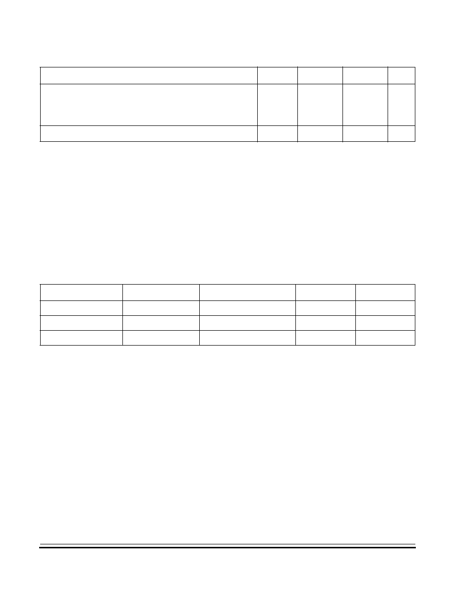
Electrical Specifications
Active Reset Characteristics
MC68HC05P18A
Technical Data
MOTOROLA
Electrical Specifications
119
NON-DISCLOSURE AGREEMENT REQUIRED
13.7 Active Reset Characteristics
EEPROM program/erase time
Byte
Block
Bulk
--
--
--
--
5
30
100
ms
Low-voltage reset inhibit
V
LVRI
3.5
4.3
V
1. V
DD
= 5.0 Vdc
±
10%, V
SS
= 0 Vdc, T
A
= ≠40
∞
C to +125
∞
C, unless otherwise noted. All values shown reflect average
measurements.
2. Run (Operating) I
DD
, wait I
DD
: Measured using external square wave clock source to OSC1 (f
OSC
= 4.2 MHz), all inputs
0.2 Vdc from rail; no DC loads, less than 50 pF on all outputs, C
L
= 20 pF on OSC2
3. Wait I
DD
: Only timer system active
Wait I
DD
is affected linearly by the OSC2 capacitance.
Wait, Stop I
DD
: All ports configured as inputs, V
IL
= 0.2 Vdc, V
IH
= V
DD
≠0.2 Vdc
Stop I
DD
measured with OSC1 = V
SS
4. Run and wait I
DD
limit values are with no load on PD5 clockout, when PD5 is enabled.
Run and wait I
DD
values are for both PD5 enabled and disabled and LVR enabled and disabled.
Characteristic
(1)
Symbol
Min
Max
Unit
Rise Time
Fall Time
Pulse Width
C
Load
Pullup
0.5
µ
s
13 ns
2.4
µ
s
59 pF
10 K
1.0
µ
s
20 ns
2.7
µ
s
100 pF
10 K
2.5
µ
s
42 ns
3.7
µ
s
250 pF
10 K
Note: V
DD
= 4.5 Vdc, V
SS
= 0 Vdc, T
A
= 125
∞
C
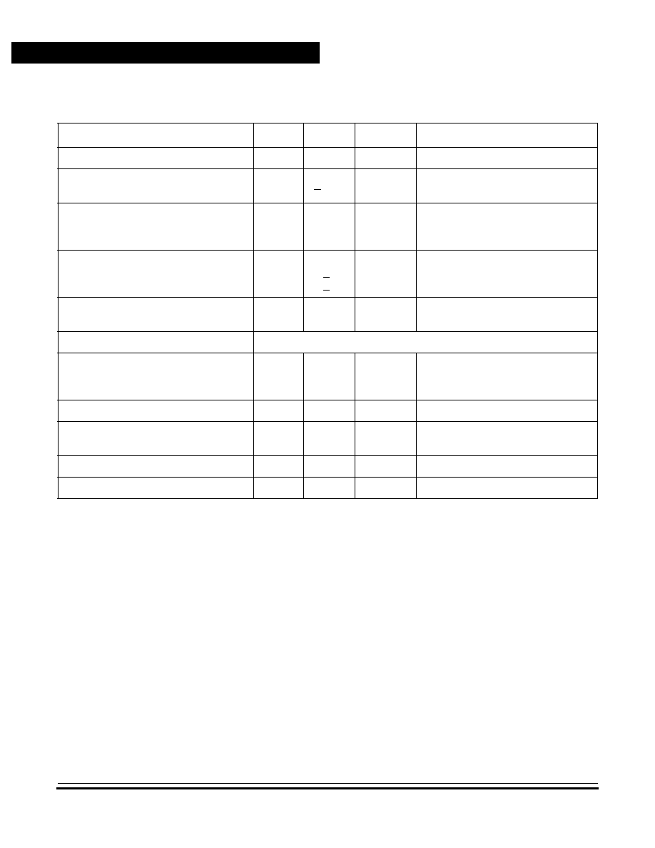
NON-DISCLOSURE AGREEMENT REQUIRED
Electrical Specifications
Technical Data
MC68HC05P18A
120
Electrical Specifications
MOTOROLA
13.8 A/D Converter Characteristics
Characteristic
(1)
1.
V
DD
= 5.0
±
10% Vdc
±
10%, V
SS
= 0 Vdc, T
A
=
-
40
∞
C to +125
∞
C, unless otherwise noted
Min
Max
Unit
Comments
Resolution
8
8
Bits
Absolute accuracy
V
DD
V
REFH
> 4.5
--
+1 1/2
LSB
Including quantization
Conversion range
V
REFH
V
SS
V
SS
V
REFH
V
DD
V
A/D accuracy may decrease
proportionately as V
REFH
is
reduced below 4.5 V.
Input leakage
AD0, AD1, AD2, AD3
V
REFH
--
--
+1
+1
µ
A
Conversion time
(2)
(Includes sampling time)
2. t
AD
= t
CYC
if clock source equals MCU
32
32
t
AD
(Note 2)
Monotonicity
Inherent (within total error)
Zero input reading
External
Internal
00
00
01
03
Hex
V
In
= 0 V
Full-scale reading
FE
FF
Hex
V
In
= V
REFH
Sample time
12
12
t
AD
(Note 3)
Input capacitance
--
12
pF
Analog input voltage
V
SS
V
REFH
V

Electrical Specifications
SIOP Timing
MC68HC05P18A
Technical Data
MOTOROLA
Electrical Specifications
121
NON-DISCLOSURE AGREEMENT REQUIRED
13.9 SIOP Timing
Figure 13-1. SIOP Timing Diagram
SDI
BIT 1 ... 6
BIT 7
BIT 0
SDO
BIT 0
BIT 1 ... 6
BIT 7
SCK
t
6
t
1
t
5
t
3
t
4
t
2
No.
Characteristic
(1)
Symbol
Min
Max
Unit
Operating frequency
(2)
Master
Slave
f
OP(
M
)
f
OP(
S
)
1
dc
1
1
f
OP
1
Cycle time
Master
Slave
t
CYC(m)
t
CYC(s)
4.0
--
4.0
4.0
t
CYC
2
SCK low time
t
CYC
238
--
ns
3
SDO data valid time
t
V
--
200
ns
4
SDO hold time
t
HO
0
--
ns
5
SDI setup time
t
S
100
--
ns
6
SDI hold time
t
H
100
--
ns
1. V
DD
= 5.0 Vdc
±
10%, V
SS
= 0 Vdc,
T
A
=
-
40
∞
C to +125
∞
C, unless otherwise noted
2. f
OP
= f
OSC
˜
2; t
CYC
= 1
˜
f
OP
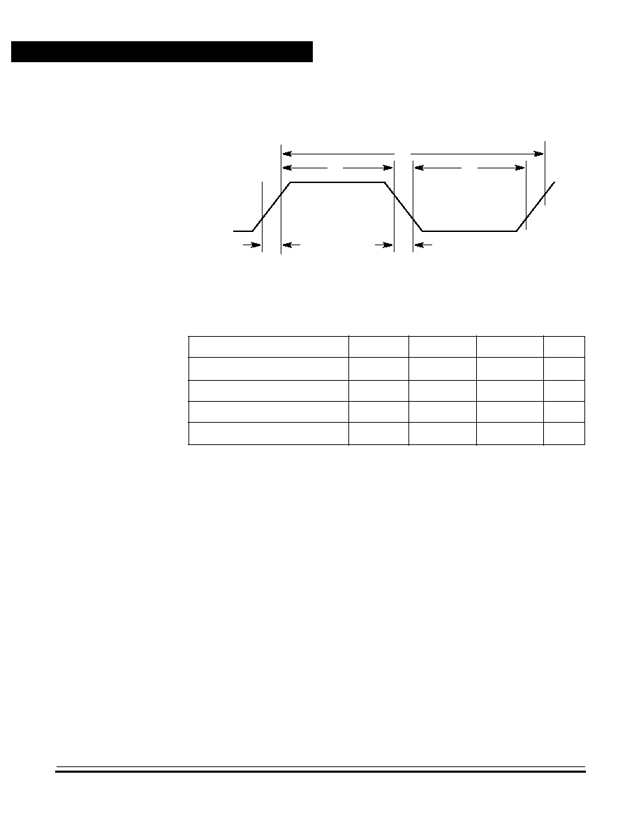
NON-DISCLOSURE AGREEMENT REQUIRED
Electrical Specifications
Technical Data
MC68HC05P18A
122
Electrical Specifications
MOTOROLA
13.10 PD5 Clock Out Timing (PD5 Clock Out Option Enabled)
Figure 13-2. PD5 Clock Out Timing
NOTE:
All timing is shown with respect to 20% and 70% V
DD
. Maximum rise and
fall times assume 44% duty cycle. Minimum rise and fall times assume
55% duty cycle.
Characteristic
Symbol
Min
Max
Unit
Cycle time
1
t
CYC
ns
Rise time
4
3.5
12
ns
Fall time
5
7.5
27.5
ns
Pulse width
2, 3
t
OH
, t
OL
--
ns
D5 CLK OUT
(4)
(5)
(2)
(1)
(3)
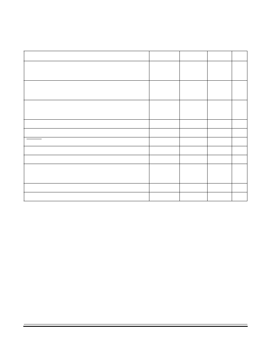
Electrical Specifications
Control Timing
MC68HC05P18A
Technical Data
MOTOROLA
Electrical Specifications
123
NON-DISCLOSURE AGREEMENT REQUIRED
13.11 Control Timing
Characteristic
(1)
1. V
DD
= 5.0 Vdc, V
SS
= 0 Vdc, T
A
= ≠40
∞
C to +125
∞
C, unless otherwise noted
Symbol
Min
Max
Unit
Frequency of operation
Crystal option
External clock source
f
OSC
--
dc
4.2
4.2
MHz
Internal operating frequency
Crystal (f
OSC
˜
2)
External clock (f
OSC
˜
2)
f
OP
--
dc
2.1
2.1
MHz
Cycle time
Low speed
High speed
t
CYC
476
238
--
ns
Crystal oscillator startup time
t
OXON
--
100
ms
Stop recovery startup time (crystal oscillator)
t
ILCH
--
100
ms
RESET pulse width
t
RL
1.5
--
t
CYC
Interrupt pulse width low (edge-triggered)
t
ILIH
125
--
ns
Interrupt pulse period
(2)
2. The minimum period, t
ILIL
, should not be less than the number of cycles it takes to execute the interrupt service routine
plus 19 t
CYC
.
t
ILIL
Note 2
--
t
CYC
OSC1 pulse width
Low speed
High speed
t
OH
, t
OL
200
100
--
ns
A/D on current stabilization time
t
ADON
--
100
µ
s
RC oscillator stabilization time
t
RCON
--
5.0
µ
s
N O N - D I S C L O S U R E A G R E E M E N T R E Q U I R E D
Technical Data
MC68HC05P18A
124
Electrical Specifications
MOTOROLA
Electr
ical Specifications
Figure 13-3. Power-On Reset and External Reset Timing Diagram
PCH
PCL
OSC1
(2)
RESET
INTERNAL
PROCESSOR
INTERNAL
ADDRESS
BUS
(1)
3FFE
3FFF
V
DD
V
DD
THRESHOLD (1-2 V TYPICAL)
t
VDDR
4064 t
CYC
t
CYC
t
RL
INTERNAL
DATA
BUS
(1)
3FFE
3FFE
3FFE
3FFE
NEW PC
3FFF
Notes:
1. Internal timing signal and bus information are not available externally.
2. OSC1 line is not meant to represent frequency. It is used only to represent time.
3. The next rising edge of the PH2 clock following the rising edge of RESET initiates the reset sequence.
NOTE 3
NEW
NEW
OP
CODE
PCL
PCH
NEW PC
NEW PC
OP
CODE
NEW PC
CLOCK
(1)

MC68HC05P18A
Technical Data
MOTOROLA
Mechanical Specifications
125
NON-DISCLOSURE AGREEMENT REQUIRED
Technical Data -- MC68HC05P18A
Section 14. Mechanical Specifications
14.1 Contents
14.2
Introduction . . . . . . . . . . . . . . . . . . . . . . . . . . . . . . . . . . . . . . .125
14.3
28-Pin Plastic Dual In-Line Package (Case #710) . . . . . . . . .126
14.4
28-Pin Small Outline Package (Case #751F) . . . . . . . . . . . . .126
14.2 Introduction
This section provides package dimension drawings for the 28-pin plastic
dual in-line (PDIP) or 28-pin small outline (SOIC) packages.
To make sure that you have the latest case outline specifications,
contact:
∑
Local Motorola Sales Office
∑
Motorola Mfax
≠
Phone 602-244-6609
≠
EMAIL rmfax0@email.sps.mot.com
∑
Worldwide Web (wwweb) at http://design-net.com
Follow Mfax or wwweb on-line instructions to retrieve the current
mechanical specifications.
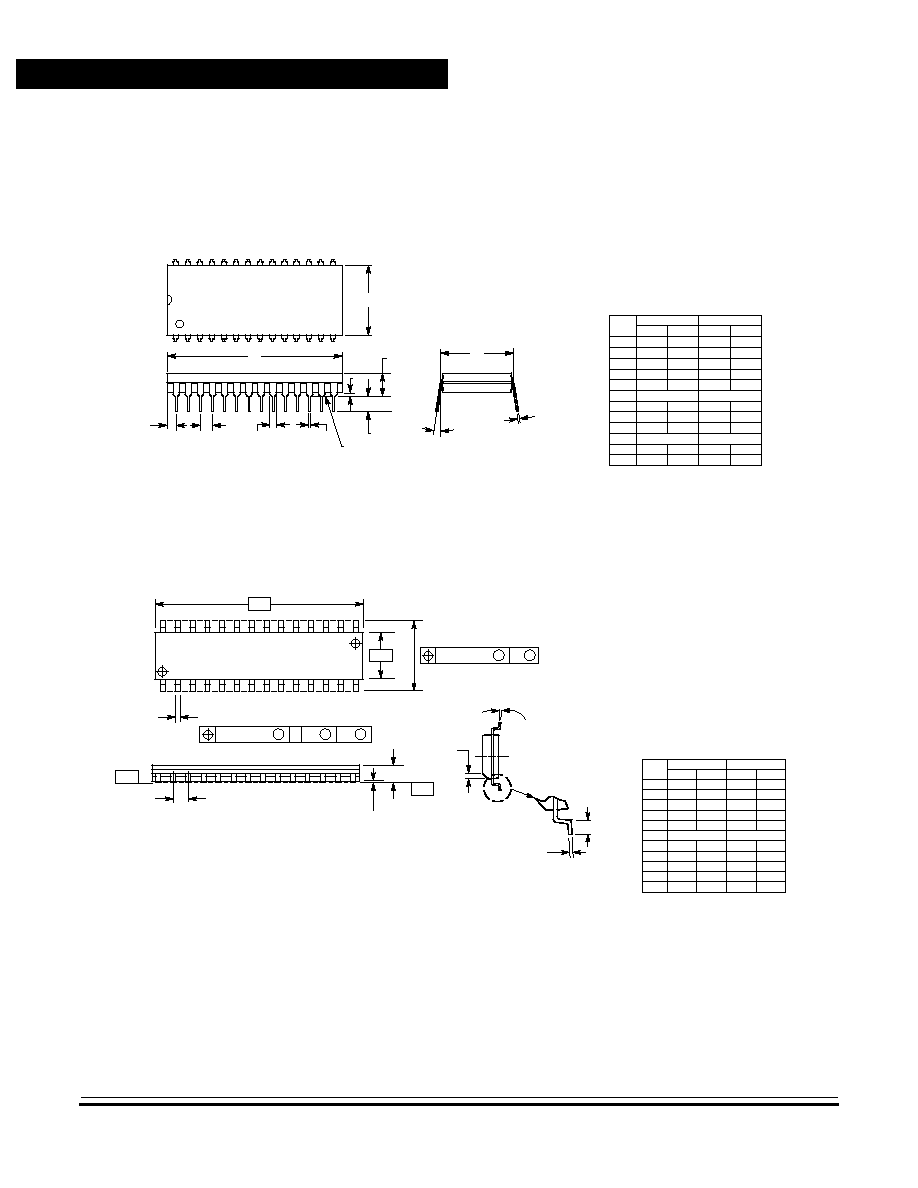
NON-DISCLOSURE AGREEMENT REQUIRED
Mechanical Specifications
Technical Data
MC68HC05P18A
126
Mechanical Specifications
MOTOROLA
14.3 28-Pin Plastic Dual In-Line Package (Case #710)
14.4 28-Pin Small Outline Package (Case #751F)
0.100 BSC
0.600 BSC
2.54 BSC
15.24 BSC
MIN
MIN
MAX
MAX
MILLIMETERS
INCHES
DIM
36.45
13.72
3.94
0.36
1.02
1.65
0.20
2.92
0
∞
0.51
37.21
14.22
5.08
0.56
1.52
2.16
0.38
3.43
15
∞
1.02
1.435
0.540
0.155
0.014
0.040
0.065
0.008
0.115
0
∞
0.020
1.465
0.560
0.200
0.022
0.060
0.085
0.015
0.135
15
∞
0.040
A
B
C
D
F
G
H
J
K
L
M
N
NOTES:
1. POSITIONAL TOLERANCE OF LEADS (D),
SHALL BE WITHIN 0.25mm (0.010) AT
MAXIMUM MATERIAL CONDITION, IN
RELATION TO SEATING PLANE AND
EACH OTHER.
2. DIMENSION L TO CENTER OF LEADS
WHEN FORMED PARALLEL.
3. DIMENSION B DOES NOT INCLUDE
MOLD FLASH.
1
14
15
28
B
A
C
N
K
M
J
D
SEATING
PLANE
F
H
G
L
MIN
MIN
MAX
MAX
MILLIMETERS
INCHES
DIM
A
B
C
D
F
G
J
K
M
P
R
17.80
7.40
2.35
0.35
0.41
0.23
0.13
0
∞
10.05
0.25
18.05
7.60
2.65
0.49
0.90
0.32
0.29
8
∞
10.55
0.75
0.701
0.292
0.093
0.014
0.016
0.009
0.005
0
∞
0.395
0.010
0.711
0.299
0.104
0.019
0.035
0.013
0.011
8
∞
0.415
0.029
1.27 BSC
0.050 BSC
NOTES:
1. DIMENSIONING AND TOLERANCING PER
ANSI Y14.5M, 1982.
2. CONTROLLING DIMENSION: MILLIMETER.
3. DIMENSION A AND B DO NOT INCLUDE MOLD
PROTRUSION.
4. MAXIMUM MOLD PROTRUSION 0.15
(0.006) PER SIDE.
5. DIMENSION D DOES NOT INCLUDE
DAMBAR PROTRUSION.
ALLOWABLE
DAMBAR PROTRUSION SHALL BE 0.13
(0.005) TOTAL IN EXCESS OF D
DIMENSION AT MAXIMUM MATERIAL
CONDITION.
-A-
-B-
1
14
15
28
-T-
C
SEATING
PLANE
0.010 (0.25)
B
M
M
M
J
-T-
K
26X
G
28X
D
14X
P
R
X 45
∞
F
0.010 (0.25)
T A
B
M
S
S
MC68HC05P18A
Technical Data
MOTOROLA
Ordering Information
127
NON-DISCLOSURE AGREEMENT REQUIRED
Technical Data -- MC68HC05P18A
Section 15. Ordering Information
15.1 Contents
15.2
Introduction . . . . . . . . . . . . . . . . . . . . . . . . . . . . . . . . . . . . . . .127
15.3
MC Order Numbers . . . . . . . . . . . . . . . . . . . . . . . . . . . . . . . .127
15.2 Introduction
This section contains instructions for ordering the MC68HC05P18A.
15.3 MC Order Numbers
Table 15-1
shows the MC order numbers for the available package
types.
Table 15-1. MC Order Numbers
MC Order Number
(1)
1. P = Plastic dual in-line package
DW = Small outline (wide body) package
Operating
Temperature Range
MC68HC05P18AP (standard)
0
∞
C to 70
∞
C
MC68HC05P18ADW (standard)
0
∞
C to 70
∞
C
MC68HC05P18ACP (extended)
≠40
∞
C to +85
∞
C
MC68HC05P18ACDW (extended)
≠40
∞
C to +85
∞
C
MC68HC05P18AMP (automotive)
≠40
∞
C to +125
∞
C
MC68HC05P18AMDW (automotive)
≠40
∞
C to +125
∞
C

NON-DISCLOSURE AGREEMENT REQUIRED
Ordering Information
Technical Data
MC68HC05P18A
128
Ordering Information
MOTOROLA


MC68HC05P18A/D
© Motorola, Inc., 1999
Motorola reserves the right to make changes without further notice to any products herein. Motorola makes no warranty, representation or guarantee regarding the suitability of its
products for any particular purpose, nor does Motorola assume any liability arising out of the application or use of any product or circuit, and specifically disclaims any and all liability,
including without limitation consequential or incidental damages. "Typical" parameters which may be provided in Motorola data sheets and/or specifications can and do vary in different
applications and actual performance may vary over time. All operating parameters, including "Typicals" must be validated for each customer application by customer's technical experts.
Motorola does not convey any license under its patent rights nor the rights of others. Motorola products are not designed, intended, or authorized for use as components in systems
intended for surgical implant into the body, or other applications intended to support or sustain life, or for any other application in which the failure of the Motorola product could create a
situation where personal injury or death may occur. Should Buyer purchase or use Motorola products for any such unintended or unauthorized application, Buyer shall indemnify and hold
Motorola and its officers, employees, subsidiaries, affiliates, and distributors harmless against all claims, costs, damages, and expenses, and reasonable attorney fees arising out of,
directly or indirectly, any claim of personal injury or death associated with such unintended or unauthorized use, even if such claim alleges that Motorola was negligent regarding the
design or manufacture of the part. Motorola and
are registered trademarks of Motorola, Inc. Motorola, Inc. is an Equal Opportunity/Affirmative Action Employer.
How to reach us:
USA/EUROPE/Locations Not Listed: Motorola Literature Distribution, P.O. Box 5405, Denver, Colorado 80217. 1-303-675-2140
or 1-800-441-2447. Customer Focus Center, 1-800-521-6274
JAPAN: Motorola Japan Ltd.; SPS, Technical Information Center, 3-20-1, Minami-Azabu, Minato-ku, Tokyo 106-8573 Japan.
81-3-3440-8573
ASIA/PACIFIC: Motorola Semiconductors H.K. Ltd.; Silicon Harbour Centre, 2 Dai King Street, Tai Po Industrial Estate,
Tai Po, N.T., Hong Kong. 852-26668334
MfaxTM, Motorola Fax Back System: RMFAX0@email.sps.mot.com; http://sps.motorola.com/mfax/;
TOUCHTONE, 1-602-244-6609; US and Canada ONLY, 1-800-774-1848
HOME PAGE: http://motorola.com/sps/
Mfax is a trademark of Motorola, Inc.