 | –≠–ª–µ–∫—Ç—Ä–æ–Ω–Ω—ã–π –∫–æ–º–ø–æ–Ω–µ–Ω—Ç: MC79M00 | –°–∫–∞—á–∞—Ç—å:  PDF PDF  ZIP ZIP |
MC79M00
Series
THREE≠TERMINAL
NEGATIVE FIXED
VOLTAGE REGULATORS
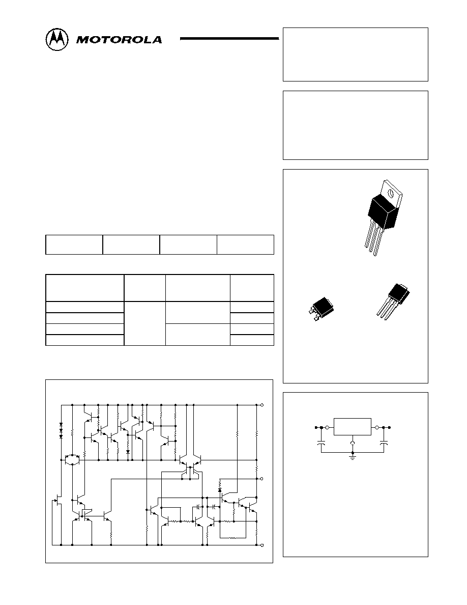
DT≠1 SUFFIX
PLASTIC PACKAGE
CASE 369
(DPAK)
DT SUFFIX
PLASTIC PACKAGE
CASE 369A
(DPAK)
Pin 1. Ground
2. Input
3. Output
STANDARD APPLICATION
A common ground is required between the input
and the output voltages. The input voltage must
remain typically 1.1 V more negative even during
the high point of the input ripple voltage.
These two digits of the type number indicate
nominal voltage.
Cin is required if regulator is located an
appreciable distance from power supply filter.
CO improve stability and transient response.
MC79MXX
Input
Cin*
0.33
µ
F
Output
CO**
1.0
µ
F
T SUFFIX
PLASTIC PACKAGE
CASE 221A
Heatsink surface
connected to Pin 2.
Heatsink surface (shown as terminal 4 in
case outline drawing) is connected to Pin 2.
3
1
2
3
1
2
3
1
XX,
*
**
Order this document by MC79M00/D
1
MOTOROLA ANALOG IC DEVICE DATA
Three-Terminal Negative
Voltage Regulators
The MC79M00 series of fixed output negative voltage regulators are
intended as complements to the popular MC78M00 series devices.
Available in fixed output voltage options of ≠5.0, ≠8.0, ≠12 and ≠15 V,
these regulators employ current limiting, thermal shutdown, and safe≠area
compensation ≠ making them remarkably rugged under most operating
conditions. With adequate heatsinking they can deliver output currents in
excess of 0.5 A.
∑
No External Components Required
∑
Internal Thermal Overload Protection
∑
Internal Short Circuit Current Limiting
∑
Output Transistor Safe≠Area Compensation
∑
Also Available in Surface Mount DPAK (DT) Package
DEVICE TYPE/NOMINAL OUTPUT VOLTAGE
MC79M05
MC79M08
≠5.0 V
≠8.0 V
MC79M12
MC79M15
≠12 V
≠15 V
ORDERING INFORMATION
Device
Output
Voltage
Tolerance
Operating
Temperature Range
Package
MC79MXXBDT, BDT≠1
4 0%
TJ = ≠ 40
∞
to +125
∞
C
DPAK
MC79MXXBT
4 0%
TJ = ≠ 40
∞
to +125
∞
C
Plastic Power
MC79MXXCDT, CDT≠1
4.0%
TJ = 0
∞
to +125
∞
C
DPAK
MC79MXXCT
TJ = 0
∞
to +125
∞
C
Plastic Power
XX indicates nominal voltage.
Representative Schematic Diagram
Gnd
VO
VI
2.4 k
25
3.6 k
1.2 k
1.1 k
2.0 k
12 k
1.0 k
4.9 k
2.0 k
14.7 k
1
1.5 k
547
2.0 k
4.0 k
0.3
10 k
10 k
20 k 20 k
20 pF
10 pF
240
750
100
2.0 k
This device contains 31 active transistors.
R1
R2
©
Motorola, Inc. 1996
Rev 4

MC79M00
2
MOTOROLA ANALOG IC DEVICE DATA
MAXIMUM RATINGS
(TA = 25
∞
C, unless otherwise noted.)
Rating
Symbol
Value
Unit
Input Voltage
VI
≠35
Vdc
Power Dissipation
Case 221A
TA = 25
∞
C
PD
Internally Limited
W
Thermal Resistance, Junction≠to≠Ambient
JA
65
∞
C/W
Thermal Resistance, Junction≠to≠Case
JC
5.0
∞
C/W
Case 369 and 369A (DPAK)
TA = 25
∞
C
PD
Internally Limited
W
Thermal Resistance, Junction≠to≠Ambient
JA
92
∞
C/W
Thermal Resistance, Junction≠to≠Case
JC
6.0
∞
C/W
Storage Junction Temperature
Tstg
≠65 to +150
∞
C
Junction Temperature
TJ
150
∞
C
NOTE: ESD data available upon request.
THERMAL CHARACTERISTICS
Characteristic
Symbol
Value
Unit
Thermal Resistance, Junction≠to≠Ambient
R
JA
65
∞
C/W
Thermal Resistance, Junction≠to≠Case
R
JC
5.0
∞
C/W
MC79M05B, C
ELECTRICAL CHARACTERISTICS
(VI = ≠10 V, IO = 350 mA, Tlow to Thigh [Note 2], unless otherwise noted.)
Characteristic
Symbol
Min
Typ
Max
Unit
Output Voltage (TJ = 25
∞
C)
VO
≠4.8
≠5.0
≠5.2
Vdc
Line Regulation, TJ = 25
∞
C (Note 1)
≠7.0 Vdc
VI
≠25 Vdc
≠8.0 Vdc
VI
≠18 Vdc
Regline
≠
≠
7.0
2.0
50
30
mV
Load Regulation, TJ = 25
∞
C (Note 1)
5.0 mA
IO
500 mA
Regload
≠
30
100
mV
Output Voltage
≠7.0 Vdc
VI
≠25 Vdc, 5.0 mA
IO
350 mA
VO
≠4.75
≠
≠5.25
Vdc
Input Bias Current (TJ = 25
∞
C)
IIB
≠
4.3
8.0
mA
Input Bias Current Change
≠8.0 Vdc
VI
≠25 Vdc, IO = 350 mA
5.0 mA
IO
350 mA, VI = ≠10 V
IIB
≠
≠
≠
≠
0.4
0.4
mA
Output Noise Voltage, TA = 25
∞
C, 10 Hz
f
100 kHz
Vn
≠
40
≠
µ
V
Ripple Rejection (f = 120 Hz)
RR
54
66
≠
dB
Dropout Voltage
IO = 500 mA, TJ = 25
∞
C
VI≠VO
≠
1.1
≠
Vdc
Average Temperature Coefficient of Output Voltage
IO = 5.0 mA, 0
∞
C
TJ
125
∞
C
VO/
T
≠
0.2
≠
mV/
∞
C
NOTES: 1. Load and line regulation are specified at constant temperature. Change in VO due to heating effects must be taken into account separately. Pulse
testing with low duty cycle is used.
2. B = Tlow to Thigh, ≠40
∞
C < TJ < 125
∞
C
C = Tlow to Thigh, 0
∞
C < TJ < 125
∞
C
MC79M00
3
MOTOROLA ANALOG IC DEVICE DATA
MC79M08B, C
ELECTRICAL CHARACTERISTICS
(VI = ≠10 V, IO = 350 mA, Tlow to Thigh [Note 2], unless otherwise noted.)
Characteristic
Symbol
Min
Typ
Max
Unit
Output Voltage (TJ = 25
∞
C)
VO
≠7.7
≠8.0
≠8.3
Vdc
Line Regulation, TJ = 25
∞
C (Note 1)
≠7.0 Vdc
VI
≠25 Vdc
≠8.0 Vdc
VI
≠18 Vdc
Regline
≠
≠
5.0
3.0
80
50
mV
Load Regulation, TJ = 25
∞
C (Note 1)
5.0 mA
IO
500 mA
Regload
≠
30
100
mV
Output Voltage
≠7.0 Vdc
VI
≠25 Vdc, 5.0 mA
IO
350 mA
VO
≠7.6
≠8.0
≠8.4
Vdc
Input Bias Current (TJ = 25
∞
C)
IIB
≠
≠
8.0
mA
Input Bias Current Change
≠8.0 Vdc
VI
≠25 Vdc, IO = 350 mA
5.0 mA
IO
350 mA, VI = ≠10 V
IIB
≠
≠
≠
≠
0.4
0.4
mA
Output Noise Voltage, TA = 25
∞
C, 10 Hz
f
100 kHz
Vn
≠
60
≠
µ
V
Ripple Rejection (f = 120 Hz)
RR
54
63
≠
dB
Dropout Voltage
IO = 500 mA, TJ = 25
∞
C
VI≠VO
≠
1.1
≠
Vdc
Average Temperature Coefficient of Output Voltage
IO = 5.0 mA, 0
∞
C
TJ
125
∞
C
VO/
T
≠
0.4
≠
mV/
∞
C
MC79M12B, C
ELECTRICAL CHARACTERISTICS
(VI = ≠19 V, IO = 350 mA, Tlow to Thigh [Note 2], unless otherwise noted.)
Characteristic
Symbol
Min
Typ
Max
Unit
Output Voltage (TJ = 25
∞
C)
VO
≠11.5
≠12
≠12.5
Vdc
Line Regulation, TJ = 25
∞
C (Note 1)
≠14.5 Vdc
VI
≠30 Vdc
≠15 Vdc
VI
≠25 Vdc
Regline
≠
≠
5.0
3.0
80
50
mV
Load Regulation, TJ = 25
∞
C (Note 1)
5.0 mA
IO
500 mA
Regload
≠
30
240
mV
Output Voltage
≠14.5 Vdc
VI
≠30 Vdc, 5.0 mA
IO
350 mA
VO
≠11.4
≠
≠12.6
Vdc
Input Bias Current (TJ = 25
∞
C)
IIB
≠
4.4
8.0
mA
Input Bias Current Change
≠14.5 Vdc
VI
≠30 Vdc, IO = 350 mA
5.0 mA
IO
350 mA, VI = ≠19 V
IIB
≠
≠
≠
≠
0.4
0.4
mA
Output Noise Voltage, TA = 25
∞
C, 10 Hz
f
100 kHz
Vn
≠
75
≠
µ
V
Ripple Rejection (f = 120 Hz)
RR
54
60
≠
dB
Dropout Voltage
IO = 500 mA, TJ = 25
∞
C
VI≠VO
≠
1.1
≠
Vdc
Average Temperature Coefficient of Output Voltage
IO = 5.0 mA, 0
∞
C
TJ
125
∞
C
VO/
T
≠
≠0.8
≠
mV/
∞
C
NOTES: 1. Load and line regulation are specified at constant temperature. Change in VO due to heating effects must be taken into account separately. Pulse
testing with low duty cycle is used.
2. B = Tlow to Thigh, ≠40
∞
C < TJ < 125
∞
C
C = Tlow to Thigh, 0
∞
C < TJ < 125
∞
C
MC79M00
4
MOTOROLA ANALOG IC DEVICE DATA
MC79M15B, C
ELECTRICAL CHARACTERISTICS
(VI = ≠ 23 V, IO = 350 mA, Tlow to Thigh [Note 2], unless otherwise noted.)
Characteristic
Symbol
Min
Typ
Max
Unit
Output Voltage (TJ = 25
∞
C)
VO
≠14.4
≠15
≠15.6
Vdc
Line Regulation, TJ = 25
∞
C (Note 1)
≠17.5 Vdc
VI
≠30 Vdc
≠18 Vdc
VI
≠28 Vdc
Regline
≠
≠
5.0
3.0
80
50
mV
Load Regulation, TJ = 25
∞
C (Note 1)
5.0 mA
IO
500 mA
Regload
≠
30
240
mV
Output Voltage
≠17.5 Vdc
VI
≠30 Vdc, 5.0 mA
IO
350 mA
VO
≠14.25
≠
≠15.75
Vdc
Input Bias Current (TJ = 25
∞
C)
IIB
≠
4.4
8.0
mA
Input Bias Current Change
≠17.5 Vdc
VI
≠30 Vdc, IO = 350 mA
5.0 mA
IO
350 mA, VI = ≠23 V
IIB
≠
≠
≠
≠
0.4
0.4
mA
Output Noise Voltage, TA = 25
∞
C, 10 Hz
f
100 kHz
Vn
≠
90
≠
µ
V
Ripple Rejection (f = 120 Hz)
RR
54
60
≠
dB
Dropout Voltage
IO = 500 mA, TJ = 25
∞
C
VI≠VO
≠
1.1
≠
Vdc
Average Temperature Coefficient of Output Voltage
IO = 5.0 mA, 0
∞
C
TJ
125
∞
C
VO/
T
≠
≠1.0
≠
mV/
∞
C
NOTES: 1. Load and line regulation are specified at constant temperature. Change in VO due to heating effects must be taken into account separately. Pulse
testing with low duty cycle is used.
2. B = Tlow to Thigh, ≠40
∞
C < TJ < 125
∞
C
C = Tlow to Thigh, 0
∞
C < TJ < 125
∞
C
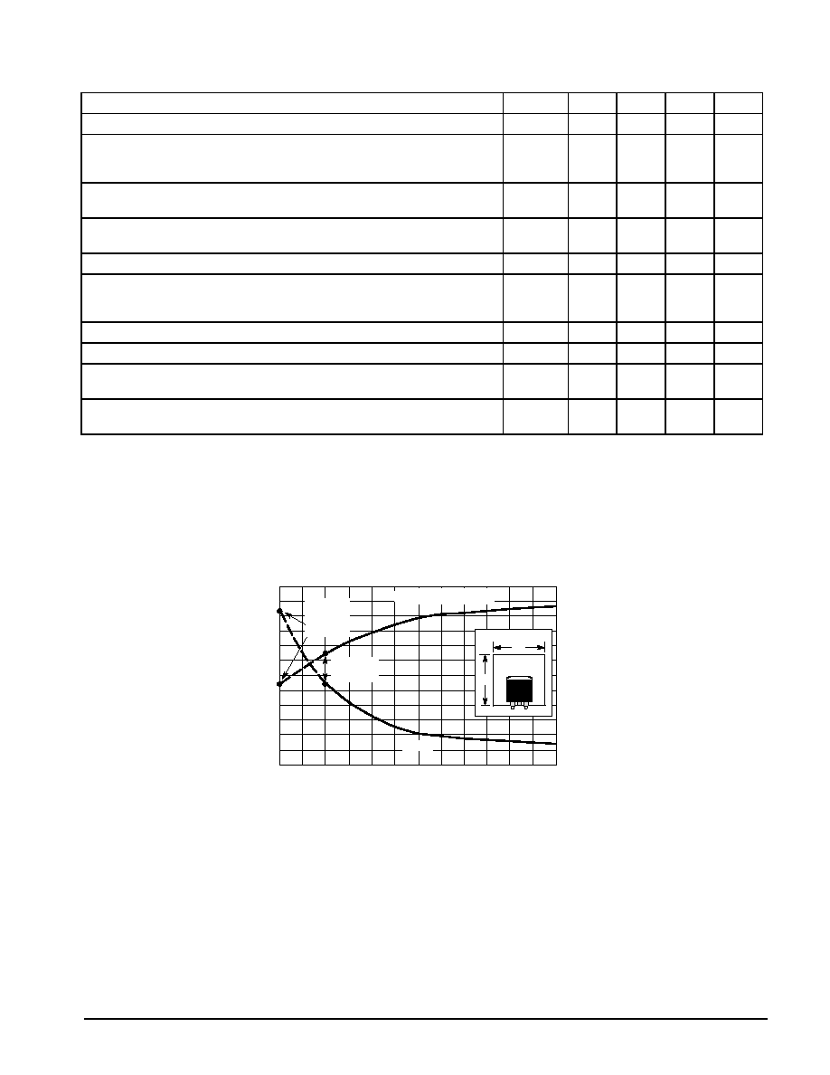
R
,
THERMAL
RESIST
ANCE
JA
JUNCTION-T
O-AIR ( C/W)
∞
P D
, MAXIMUM POWER DISSIP
A
TION (W)
Figure 1. DPAK Thermal Resistance and Maximum
Power Dissipation versus P.C.B. Copper Length
40
50
60
70
80
90
100
0
10
20
30
25
15
5.0
L, LENGTH OF COPPER (mm)
Minimum
Size Pad
L
Free Air
Mounted
Vertically
R
JA
2.0 oz. Copper
L
ŒŒŒŒ
ŒŒŒŒ
ŒŒŒŒ
0
0.4
0.8
1.2
1.6
2.0
2.4
PD(max) for TA = 50
∞
C
MC79M00
5
MOTOROLA ANALOG IC DEVICE DATA
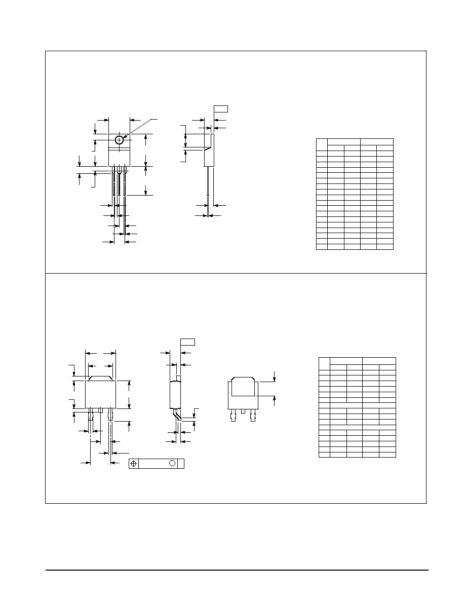
T SUFFIX
PLASTIC PACKAGE
CASE 221A≠06
ISSUE Y
OUTLINE DIMENSIONS
DT SUFFIX
PLASTIC PACKAGE
CASE 369A≠13
(DPAK)
ISSUE Y
NOTES:
1. DIMENSIONING AND TOLERANCING PER ANSI
Y14.5M, 1982.
2. CONTROLLING DIMENSION: INCH.
3. DIMENSION Z DEFINES A ZONE WHERE ALL
BODY AND LEAD IRREGULARITIES ARE
ALLOWED.
DIM
MIN
MAX
MIN
MAX
MILLIMETERS
INCHES
A
0.570
0.620
14.48
15.75
B
0.380
0.405
9.66
10.28
C
0.160
0.190
4.07
4.82
D
0.025
0.035
0.64
0.88
F
0.142
0.147
3.61
3.73
G
0.095
0.105
2.42
2.66
H
0.110
0.155
2.80
3.93
J
0.018
0.025
0.46
0.64
K
0.500
0.562
12.70
14.27
L
0.045
0.060
1.15
1.52
N
0.190
0.210
4.83
5.33
Q
0.100
0.120
2.54
3.04
R
0.080
0.110
2.04
2.79
S
0.045
0.055
1.15
1.39
T
0.235
0.255
5.97
6.47
U
0.000
0.050
0.00
1.27
V
0.045
≠≠≠
1.15
≠≠≠
Z
≠≠≠
0.080
≠≠≠
2.04
B
Q
H
Z
L
V
G
N
A
K
F
1
2 3
4
D
SEATING
PLANE
≠T≠
C
S
T
U
R
J
D
A
K
B
R
V
S
F
L
G
2 PL
M
0.13 (0.005)
T
E
C
U
J
H
≠T≠
SEATING
PLANE
Z
DIM
MIN
MAX
MIN
MAX
MILLIMETERS
INCHES
A
0.235
0.250
5.97
6.35
B
0.250
0.265
6.35
6.73
C
0.086
0.094
2.19
2.38
D
0.027
0.035
0.69
0.88
E
0.033
0.040
0.84
1.01
F
0.037
0.047
0.94
1.19
G
0.180 BSC
4.58 BSC
H
0.034
0.040
0.87
1.01
J
0.018
0.023
0.46
0.58
K
0.102
0.114
2.60
2.89
L
0.090 BSC
2.29 BSC
R
0.175
0.215
4.45
5.46
S
0.020
0.050
0.51
1.27
U
0.020
≠≠≠
0.51
≠≠≠
V
0.030
0.050
0.77
1.27
Z
0.138
≠≠≠
3.51
≠≠≠
NOTES:
1. DIMENSIONING AND TOLERANCING PER ANSI
Y14.5M, 1982.
2. CONTROLLING DIMENSION: INCH.
1
2
3
4