 | –≠–ª–µ–∫—Ç—Ä–æ–Ω–Ω—ã–π –∫–æ–º–ø–æ–Ω–µ–Ω—Ç: MCR703A | –°–∫–∞—á–∞—Ç—å:  PDF PDF  ZIP ZIP |

1
Motorola Thyristor Device Data
Silicon Controlled Rectifiers
Reverse Blocking Triode Thyristors
. . . PNPN devices designed for high volume, low cost consumer applications such as
temperature, light and speed control; process and remote control; and warning
systems where reliability of operation is critical.
∑
Small Size
∑
Passivated Die Surface for Reliability and Uniformity
∑
Low Level Triggering and Holding Characteristics
∑
Recommend Electrical Replacement for C106
∑
Available in Two Package Styles:
Surface Mount Leadforms -- Case 369A
Miniature Plastic Package -- Straight Leads -- Case 369
ORDERING INFORMATION
∑
To Obtain "DPAK" in Surface Mount Leadform (Case 369A):
Shipped in Sleeves -- No Suffix, i.e., MCR706A
Shipped in 16 mm Tape and Reel -- Add "RL" Suffix to Device Number, i.e.,
MCR706ARL
∑
To Obtain "DPAK" in Straight Lead Version:
Shipped in Sleeves -- Add `1' Suffix to Device Number, i.e., MCR706A1
MAXIMUM RATINGS
(TJ = 25
∞
C unless otherwise noted.)
Characteristic
Symbol
Value
Unit
Peak Repetitive Forward and Reverse Blocking Voltage
(1)
(1/2 Sine Wave)
(RGK = 1000 Ohms,
MCR703A1, MCR703A
TC = ≠40 to +110
∞
C)
MCR704A1, MCR704A
MCR706A1, MCR706A
MCR708A1, MCR708A
VDRM
or
VRRM
100
200
400
600
Volts
Peak Non-repetitive Reverse Blocking Voltage
(1/2 Sine Wave, RGK = 1000 Ohms,
TC = ≠40 to +110
∞
C)
MCR703A1, MCR703A
MCR704A1, MCR704A
MCR706A1, MCR706A
MCR708A1, MCR708A
VRSM
150
250
450
650
Volts
Average On-State Current
(TC = ≠40 to +90
∞
C)
(TC = +100
∞
C)
IT(AV)
2.6
1.6
Amps
Surge On-State Current (1/2 Sine Wave, 60 Hz, TC =
+90
∞
C)
(1/2 Sine Wave, 1.5 ms TC =
+90
∞
C)
ITSM
25
35
Amps
Circuit Fusing (t = 8.3 ms)
I2t
2.6
A2s
Peak Gate Power (Pulse Width = 10
µ
s, TC = 90
∞
C)
PGM
0.5
Watt
Average Gate Power (t = 8.3 ms, TC = 90
∞
C)
PG(AV)
0.1
Watt
Peak Forward Gate Current
IGM
0.2
Amp
Peak Reverse Gate Voltage
VRGM
6
Volts
Operating Junction Temperature Range
TJ
≠40 to +110
∞
C
Storage Temperature Range
Tstg
≠40 to +150
∞
C
1. VDRM and VRRM for all types can be applied on a continuous basis. Ratings apply for zero or
negative gate voltage; however, positive gate voltage shall not be applied concurrent with
negative potential on the anode. Blocking voltages shall not be tested with a constant current
source such that the voltage ratings of the devices are exceeded.
Preferred devices are Motorola recommended choices for future use and best overall value.
Order this document
by MCR703A/D
MOTOROLA
SEMICONDUCTOR TECHNICAL DATA
©
Motorola, Inc. 1995
REV 1
MCR703A
thru
MCR708A
CASE 369A
STYLE 5
SCRs
4.0 AMPERES RMS
100 thru 600 VOLTS
CASE 369
STYLE 5
A
A
K
G
K
A
A
G
Figure 1. Minimum Pad
Sizes for
Surface Mounting
*Motorola preferred devices
K
G
A
0.165
4.191
0.243
6.172
0.190
4.826
inches
mm
0.063
1.6
0.100
2.54
0.1
18
3.0
*
MCR703A thru MCR708A
2
Motorola Thyristor Device Data
THERMAL CHARACTERISTICS
Characteristic
Symbol
Min
Max
Unit
Thermal Resistance, Junction to Case
R
JC
--
8.33
∞
C/W
Thermal Resistance, Junction to Ambient (Case 369A-04)(1)
R
JA
--
80
∞
C/W
Thermal Resistance, Junction to Ambient (Case 369-03)(2)
R
JA
--
85
∞
C/W
ELECTRICAL CHARACTERISTICS
(TC = 25
∞
C and RGK = 1000 ohms unless otherwise noted.)
Characteristic
Symbol
Min
Typ
Max
Unit
Peak Forward or Reverse Blocking Current
(VAK = Rated VDRM or VRRM) TC = 25
∞
C
TC = 110
∞
C
IDRM, IRRM
--
--
--
10
200
µ
A
Peak Forward "On" Voltage
(ITM = 8.2 A Peak, Pulse Width = 1 to 2 ms, 2% Duty Cycle)
VTM
--
--
2.2
Volts
Gate Trigger Current (Continuous dc)(3)
(VAK = 12 Vdc, RL = 24 Ohms)
(VAK = 12 Vdc, RL = 24 Ohms, TC = ≠40
∞
C)
IGT
--
--
25
--
75
300
µ
A
Gate Trigger Voltage (Continuous dc)
(Source Voltage = 12 V, RS = 50 Ohms)
(VAK = 12 Vdc, RL = 24 Ohms, TC = ≠40
∞
C)
VGT
--
--
1
Volts
Gate Non-Trigger Voltage
(VAK = Rated VDRM, RL = 100 Ohms, TC = 110
∞
C)
VGD
0.2
--
--
Volts
Holding Current
(VAK = 12 Vdc, IGT = 2 mA)
TC = 25
∞
C
(Initiating On-State Current = 200 mA) TC = ≠40
∞
C
IH
--
--
--
--
5
10
mA
Total Turn-On Time
(Source Voltage = 12 V, RS = 6 k Ohms)
(ITM = 8.2 A, IGT = 2 mA, Rated VDRM)
(Rise Time = 20 ns, Pulse Width = 10
µ
s)
tgt
--
2
--
µ
s
Forward Voltage Application Rate
(VD = Rated VDRM, Exponential Waveform, TC = 110
∞
C)
dv/dt
--
10
--
V/
µ
s
1. Case 369A-04 when surface mounted on minimum pad sizes recommended.
2. Case 369-03 standing in free air.
3. RGK current not included in measurement.
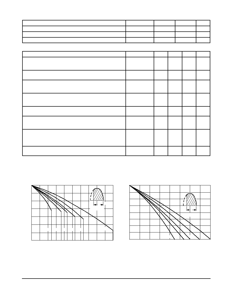
Figure 2. Maximum Case Temperature
Figure 3. Maximum Ambient Temperature
f = 60 Hz
3.6
0
0.4
0.8
1.2
1.6
2
2.4
2.8
106
3.2
82
86
90
98
102
94
120
∞
= 30
∞
110
4
180
∞
IT(AV), AVERAGE FORWARD CURRENT (AMP)
60
∞
0
0.8
0
f = 60 Hz
60
∞
90
∞
180
∞
dc
90
∞
90
0
0.1
0.2
0.3
0.4
0.6
0.5
30
50
70
110
0.7
IT(AV), AVERAGE FORWARD CURRENT (AMP)
dc
= 30
∞
T
, MAXIMUM
ALLOW
ABLE CASE
TEMPERA
TURE ( C)
C
∞
T
, MAXIMUM
ALLOW
ABLE
AMBIENT
A
TEMPERA
TURE ( C)
∞
MCR703A thru MCR708A
3
Motorola Thyristor Device Data
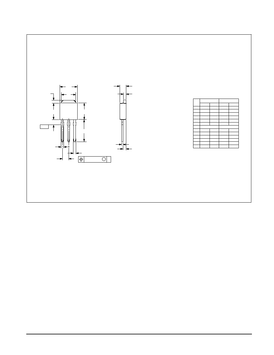
PACKAGE DIMENSIONS
CASE 369
NOTES:
1. DIMENSIONING AND TOLERANCING PER ANSI
Y14.5M, 1982.
2. CONTROLLING DIMENSION: INCH.
STYLE 5:
PIN 1. GATE
2. ANODE
3. CATHODE
4. ANODE
1
2
3
4
V
S
A
K
≠T≠
SEATING
PLANE
R
B
F
G
D
3 PL
M
0.13 (0.005)
T
C
E
J
H
DIM
MIN
MAX
MIN
MAX
MILLIMETERS
INCHES
A
0.235
0.250
5.97
6.35
B
0.250
0.265
6.35
6.73
C
0.086
0.094
2.19
2.38
D
0.027
0.035
0.69
0.88
E
0.033
0.040
0.84
1.01
F
0.037
0.047
0.94
1.19
G
0.090 BSC
2.29 BSC
H
0.034
0.040
0.87
1.01
J
0.018
0.023
0.46
0.58
K
0.350
0.380
8.89
9.65
R
0.175
0.215
4.45
5.46
S
0.050
0.090
1.27
2.28
V
0.030
0.050
0.77
1.27
MCR703A thru MCR708A
4
Motorola Thyristor Device Data
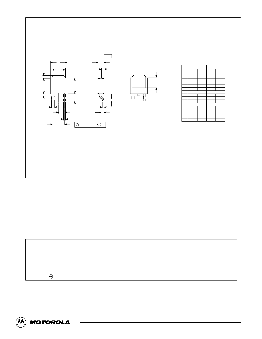
CASE 369A
STYLE 5:
PIN 1. GATE
2. ANODE
3. CATHODE
4. ANODE
D
A
K
B
R
V
S
F
L
G
2 PL
M
0.13 (0.005)
T
E
C
U
J
H
≠T≠
SEATING
PLANE
Z
DIM
MIN
MAX
MIN
MAX
MILLIMETERS
INCHES
A
0.235
0.250
5.97
6.35
B
0.250
0.265
6.35
6.73
C
0.086
0.094
2.19
2.38
D
0.027
0.035
0.69
0.88
E
0.033
0.040
0.84
1.01
F
0.037
0.047
0.94
1.19
G
0.180 BSC
4.58 BSC
H
0.034
0.040
0.87
1.01
J
0.018
0.023
0.46
0.58
K
0.102
0.114
2.60
2.89
L
0.090 BSC
2.29 BSC
R
0.175
0.215
4.45
5.46
S
0.020
0.050
0.51
1.27
U
0.020
≠≠≠
0.51
≠≠≠
V
0.030
0.050
0.77
1.27
Z
0.138
≠≠≠
3.51
≠≠≠
NOTES:
1. DIMENSIONING AND TOLERANCING PER ANSI
Y14.5M, 1982.
2. CONTROLLING DIMENSION: INCH.
1
2
3
4
Motorola reserves the right to make changes without further notice to any products herein. Motorola makes no warranty, representation or guarantee regarding
the suitability of its products for any particular purpose, nor does Motorola assume any liability arising out of the application or use of any product or circuit, and
specifically disclaims any and all liability, including without limitation consequential or incidental damages. "Typical" parameters can and do vary in different
applications. All operating parameters, including "Typicals" must be validated for each customer application by customer's technical experts. Motorola does
not convey any license under its patent rights nor the rights of others. Motorola products are not designed, intended, or authorized for use as components in
systems intended for surgical implant into the body, or other applications intended to support or sustain life, or for any other application in which the failure of
the Motorola product could create a situation where personal injury or death may occur. Should Buyer purchase or use Motorola products for any such
unintended or unauthorized application, Buyer shall indemnify and hold Motorola and its officers, employees, subsidiaries, affiliates, and distributors harmless
against all claims, costs, damages, and expenses, and reasonable attorney fees arising out of, directly or indirectly, any claim of personal injury or death
associated with such unintended or unauthorized use, even if such claim alleges that Motorola was negligent regarding the design or manufacture of the part.
Motorola and
are registered trademarks of Motorola, Inc. Motorola, Inc. is an Equal Opportunity/Affirmative Action Employer.
Literature Distribution Centers:
USA: Motorola Literature Distribution; P.O. Box 20912; Phoenix, Arizona 85036.
EUROPE: Motorola Ltd.; European Literature Centre; 88 Tanners Drive, Blakelands, Milton Keynes, MK14 5BP, England.
JAPAN: Nippon Motorola Ltd.; 4-32-1, Nishi-Gotanda, Shinagawa-ku, Tokyo 141, Japan.
ASIA PACIFIC: Motorola Semiconductors H.K. Ltd.; Silicon Harbour Center, No. 2 Dai King Street, Tai Po Industrial Estate, Tai Po, N.T., Hong Kong.
MCR703A/D
*MCR703A/D*