 | –≠–ª–µ–∫—Ç—Ä–æ–Ω–Ω—ã–π –∫–æ–º–ø–æ–Ω–µ–Ω—Ç: MGP7N60ED | –°–∫–∞—á–∞—Ç—å:  PDF PDF  ZIP ZIP |
1
Motorola IGBT Device Data
Designer's
TM
Data Sheet
Insulated Gate Bipolar Transistor
with Anti-Parallel Diode
N≠Channel Enhancement≠Mode Silicon Gate
This Insulated Gate Bipolar Transistor (IGBT) is co≠packaged
with a soft recovery ultra≠fast rectifier and uses an advanced
termination scheme to provide an enhanced and reliable high
voltage≠blocking capability. Its new 600 V IGBT technology is
specifically suited for applications requiring both a high tempera-
ture short circuit capability and a low VCE(on). It also provides fast
switching characteristics and results in efficient operation at high
frequencies. Co≠packaged IGBTs save space, reduce assembly
time and cost. This new E≠series introduces an energy efficient,
ESD protected, and short circuit rugged device.
∑
Industry Standard TO≠220 Package
∑
High Speed: Eoff = 70
m
J/A typical at 125
∞
C
∑
High Voltage Short Circuit Capability ≠ 10
m
s minimum at 125
∞
C, 400 V
∑
Low On≠Voltage 2.0 V typical at 5.0 A, 125
∞
C
∑
Soft Recovery Free Wheeling Diode
is Included in the Package
∑
Robust High Voltage Termination
∑
ESD Protection Gate≠Emitter Zener Diodes
MAXIMUM RATINGS
(TJ = 25
∞
C unless otherwise noted)
Rating
Symbol
Value
Unit
Collector≠Emitter Voltage
VCES
600
Vdc
Collector≠Gate Voltage (RGE = 1.0 M
)
VCGR
600
Vdc
Gate≠Emitter Voltage -- Continuous
VGE
±
20
Vdc
Collector Current -- Continuous @ TC = 25
∞
C
-- Continuous @ TC = 90
∞
C
-- Repetitive Pulsed Current (1)
IC25
IC90
ICM
10
7.0
14
Adc
Apk
Total Power Dissipation @ TC = 25
∞
C
Derate above 25
∞
C
PD
81
0.65
Watts
W/
∞
C
Operating and Storage Junction Temperature Range
TJ, Tstg
≠ 55 to 150
∞
C
Short Circuit Withstand Time
(VCC = 400 Vdc, VGE = 15 Vdc, TJ = 125
∞
C, RG = 20
)
tsc
10
m
s
Thermal Resistance -- Junction to Case ≠ IGBT
-- Junction to Case ≠ Diode
-- Junction to Ambient
R
JC
R
JC
R
JA
1.5
2.7
65
∞
C/W
Maximum Lead Temperature for Soldering Purposes, 1/8
from case for 5 seconds
TL
260
∞
C
Mounting Torque, 6≠32 or M3 screw
10 lbf
S
in (1.13 N
S
m)
(1) Pulse width is limited by maximum junction temperature. Repetitive rating.
Designer's Data for "Worst Case" Conditions -- The Designer's Data Sheet permits the design of most circuits entirely from the information presented. SOA Limit
curves -- representing boundaries on device characteristics -- are given to facilitate "worst case" design.
Designer's
TM
is a trademark of Motorola, Inc.
REV 1
Order this document
by MGP7N60ED/D
MOTOROLA
SEMICONDUCTOR TECHNICAL DATA
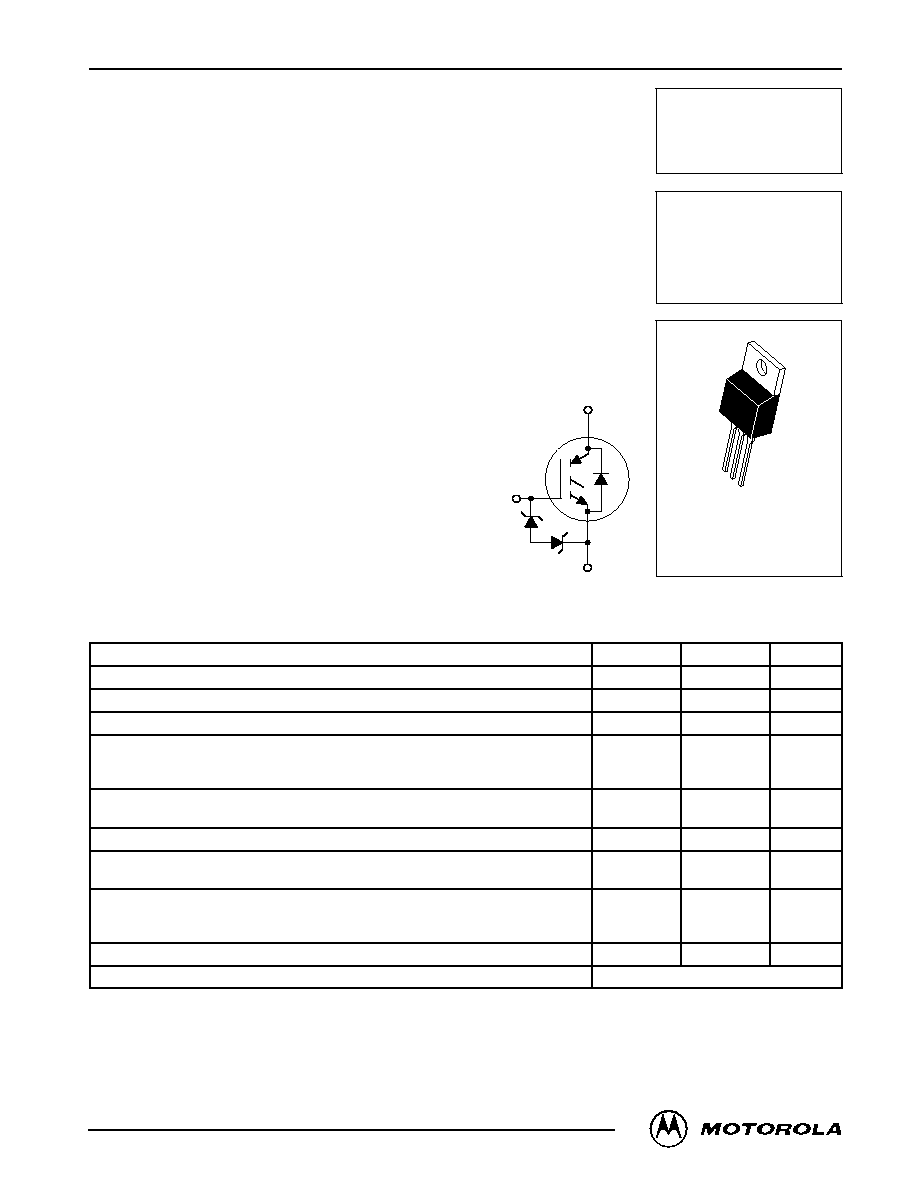
MGP7N60ED
IGBT & DIODE IN TO≠220
7.0 A @ 90
∞
C
10 A @ 25
∞
C
600 VOLTS
SHORT CIRCUIT RATED
LOW ON≠VOLTAGE
CASE 221A≠09
STYLE 9
TO≠220AB
C
E
G
G
C
E
©
Motorola, Inc. 1998

MGP7N60ED
2
Motorola IGBT Device Data
ELECTRICAL CHARACTERISTICS
(TJ = 25
∞
C unless otherwise noted)
Characteristic
Symbol
Min
Typ
Max
Unit
OFF CHARACTERISTICS
Collector≠to≠Emitter Breakdown Voltage
(VGE = 0 Vdc, IC = 25
µ
Adc)
Temperature Coefficient (Positive)
V(BR)CES
600
--
--
870
--
--
Vdc
mV/
∞
C
Zero Gate Voltage Collector Current
(VCE = 600 Vdc, VGE = 0 Vdc)
(VCE = 600 Vdc, VGE = 0 Vdc, TJ = 125
∞
C)
ICES
--
--
--
--
10
200
µ
Adc
Gate≠Body Leakage Current (VGE =
±
20 Vdc, VCE = 0 Vdc)
IGES
--
--
50
m
Adc
ON CHARACTERISTICS (1)
Collector≠to≠Emitter On≠State Voltage
(VGE = 15 Vdc, IC = 2.5 Adc)
(VGE = 15 Vdc, IC = 2.5 Adc, TJ = 125
∞
C)
(VGE = 15 Vdc, IC = 5.0 Adc)
VCE(on)
--
--
--
1.6
1.5
2.0
1.9
--
2.4
Vdc
Gate Threshold Voltage
(VCE = VGE, IC = 1.0 mAdc)
Threshold Temperature Coefficient (Negative)
VGE(th)
4.0
--
6.0
10
8.0
--
Vdc
mV/
∞
C
Forward Transconductance (VCE = 10 Vdc, IC = 5.0 Adc)
gfe
--
2.5
--
Mhos
DYNAMIC CHARACTERISTICS
Input Capacitance
(V
25 Vdc V
0 Vdc
Cies
--
610
--
pF
Output Capacitance
(VCE = 25 Vdc, VGE = 0 Vdc,
f = 1.0 MHz)
Coes
--
60
--
Transfer Capacitance
f = 1.0 MHz)
Cres
--
10
--
SWITCHING CHARACTERISTICS (1)
Turn≠On Delay Time
(V
360 Vd
I
5 0 Ad
td(on)
--
22
--
ns
Rise Time
(V
360 Vd
I
5 0 Ad
tr
--
24
--
Turn≠Off Delay Time
(VCC = 360 Vdc, IC = 5.0 Adc,
V
15 Vd
L
300 H
td(off)
--
64
--
Fall Time
VGE = 15 Vdc, L = 300
m
H,
RG = 20
)
tf
--
196
--
Turn≠Off Switching Loss
RG = 20
)
Energy losses include "tail"
Eoff
--
200
340
m
J
Turn≠On Switching Loss
Eon
--
71
--
Total Switching Loss
Ets
--
271
--
Turn≠On Delay Time
(V
360 Vd
I
5 0 Ad
td(on)
--
31
--
ns
Rise Time
(V
360 Vd
I
5 0 Ad
tr
--
24
--
Turn≠Off Delay Time
(VCC = 360 Vdc, IC = 5.0 Adc,
V
15 Vd
L
300 H
td(off)
--
195
--
Fall Time
VGE = 15 Vdc, L = 300
m
H,
RG = 20
,
TJ = 125
∞
C)
tf
--
220
--
Turn≠Off Switching Loss
RG = 20
,
TJ = 125 C)
Energy losses include "tail"
Eoff
--
350
--
m
J
Turn≠On Switching Loss
Eon
--
135
--
Total Switching Loss
Ets
--
485
--
Gate Charge
(V
360 Vdc I
5 0 Adc
QT
--
27.2
--
nC
(VCC = 360 Vdc, IC = 5.0 Adc,
VGE = 15 Vdc)
Q1
--
7.0
--
VGE = 15 Vdc)
Q2
--
13.7
--
(1) Pulse Test: Pulse Width
300
µ
s, Duty Cycle
2%.

MGP7N60ED
3
Motorola IGBT Device Data
DIODE CHARACTERISTICS
Diode Forward Voltage Drop
(IEC = 2.3 Adc)
(IEC = 2.3 Adc, TJ = 125
∞
C)
(IEC = 4.6 Adc)
VFEC
--
--
--
1.7
1.3
2.0
--
--
2.3
Vdc
Reverse Recovery Time
(I
4 6 Ad
trr
--
40
--
ns
(IF = 4.6 Adc,
VR = 360 Vdc
ta
--
17
--
VR = 360 Vdc,
dIF/dt = 200 A/
m
s)
tb
--
23
--
Reverse Recovery Stored Charge
F
m
)
QRR
--
60
--
nC
Reverse Recovery Time
(IF = 4 6 Adc
trr
--
105
--
ns
(IF = 4.6 Adc,
VR = 360 Vdc,
ta
--
36
--
R
,
dIF/dt = 200 A/
m
s,
TJ = 125
∞
C)
tb
--
69
--
Reverse Recovery Stored Charge
TJ = 125
∞
C)
QRR
--
247
--
nC
INTERNAL PACKAGE INDUCTANCE
Internal Emitter Inductance
(Measured from the emitter lead 0.25
from package to emitter bond pad)
LE
--
7.5
--
nH
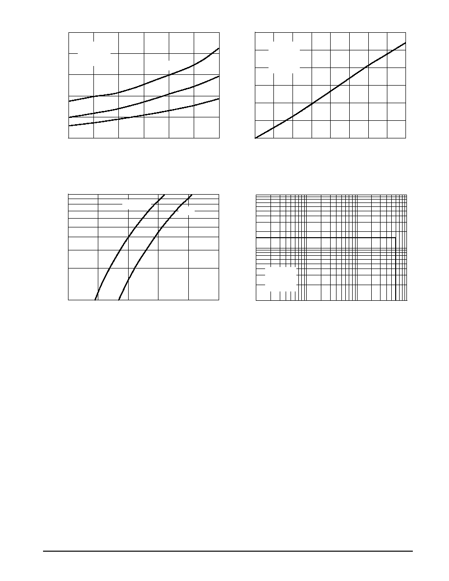
Figure 1. Output Characteristics
Figure 2. Output Characteristics
Figure 3. Transfer Characteristics
Figure 4. Collector≠To≠Emitter Saturation
Voltage versus Junction Temperature
8
0
VCE, COLLECTOR≠TO≠EMITTER VOLTAGE (VOLTS)
15
20
10
I C
, COLLECT
OR
CURRENT
(AMPS)
5
0
3
1
2
4
5
6
7
8
0
VCE, COLLECTOR≠TO≠EMITTER VOLTAGE (VOLTS)
15
20
10
I C
, COLLECT
OR
CURRENT
(AMPS)
5
0
3
1
2
4
5
6
7
TJ = 25
∞
C
VGE = 10 V
12.5 V
15 V
17.5 V
20 V
TJ = 125
∞
C
VGE = 10 V
12.5 V
15 V
17.5 V
20 V
10
12
5
VGE, GATE≠TO≠EMITTER VOLTAGE (VOLTS)
12
8
6
4
2
0
TJ, JUNCTION TEMPERATURE (
∞
C)
≠25
≠50
2.2
1.8
1.6
1.4
1.2
1.0
0
11
V
CE(on)
, COLLECT
OR≠T
O≠EMITTER ON≠ST
A
T
E
6
7
8
9
25
50
75
100
125
150
I C
, COLLECT
OR
CURRENT
(AMPS)
13
10
2.0
IC = 5.0 A
3.75 A
2.5 A
TJ = 125
∞
C
25
∞
C
VOL
T
AGE (VOL
TS)
VCE = 100 V
5
m
S PULSE WIDTH
VGE = 15 V
80
m
S PULSE WIDTH

MGP7N60ED
4
Motorola IGBT Device Data
Figure 5. Capacitance Variation
Figure 6. Gate≠To≠Emitter Voltage versus
Total Charge
Figure 7. Total Energy Losses versus
Gate Resistance
Figure 8. Total Energy Losses versus
Junction Temperature
45
5
RG, GATE RESISTANCE (OHMS)
0.50
0.45
0.40
TJ, JUNCTION TEMPERATURE (
∞
C)
150
0.2
0
,
T
O
T
A
L
ENERGY
LOSSES (mJ)
0.20
15
25
0
25
0.4
35
50
75
100
125
TJ = 125
∞
C
VDD = 360 V
VGE = 15 V
IC = 5.0 A
3.75 A
2.5 A
VCC = 360 V
VGE = 15 V
RG = 20
W
IC = 5.0 A
0.25
E
TS
Figure 9. Total Energy Losses versus
Collector Current
Figure 10. Turn≠Off Losses versus
Gate Resistance
7
8
0
IC, COLLECTOR CURRENT (AMPS)
0.4
0
2
0.6
0.2
TJ = 125
∞
C
VDD = 360 V
VGE = 15 V
RG = 20
W
4
5
,
T
O
T
A
L
ENERGY
LOSSES (mJ)
E
TS
,
T
O
T
A
L
ENERGY
LOSSES (mJ)
E
TS
0.15
0.55
0.60
0.6
0.3
0.1
0.5
0.5
0.1
0.7
0.3
0.8
10
0
VCE, COLLECTOR≠TO≠EMITTER VOLTAGE (VOLTS)
1200
800
600
400
200
0
Qg, TOTAL GATE CHARGE (nC)
5
30
0
20
16
12
4
0
5
C, CAP
ACIT
ANCE
(pF)
15
25
20
1000
10
15
35
20
25
8
V
, GA
TE≠T
O≠EMITTER
VOL
T
AGE
(VOL
TS)
GE
TJ = 25
∞
C
IC = 5.0 A
Q1
Q2
QT
VGE = 0 V
TJ = 25
∞
C
Cies
Coes
Cres
50
10
GATE RESISTANCE (OHMS)
0.4
0.5
0.3
0.1
0
25
15
20
30
35
40
45
0.2
VCC = 360 V
VGE = 15 V
TJ = 125
∞
C
IC = 5.0 A
3.75 A
2.5 A
,
TURN≠OFF
ENERGY
LOSSES (mJ)
E
of
f
0.30
0.35
3.75 A
2.5 A
1
3
6
MGP7N60ED
5
Motorola IGBT Device Data
Figure 11. Turn≠Off Losses versus
Junction Temperature
Figure 12. Turn≠Off Losses versus
Collector Current
Figure 13. Forward Characteristics
versus Current
Figure 14. Reverse Biased Safe
Operating Area
VFM, FORWARD VOLTAGE DROP (VOLTS)
0.5
10
1
I F
, INST
ANT
ANEOUS
FOR
W
ARD
1
2
2.5
TJ = 125
∞
C
25
∞
C
1.5
CURRENT
(AMPS)
3
150
0
TJ, JUNCTION TEMPERATURE (
∞
C)
0.3
0.5
0.2
0.1
0
50
25
75
100
125
0.4
VCC = 360 V
VGE = 15 V
RG = 20
W
IC = 5.0 A
3.75 A
2.5 A
,
TURN≠OFF
ENERGY
LOSSES (mJ)
E
of
f
5
7
0
IC, COLLECTOR CURRENT (AMPS)
0.6
0.4
0.3
0.2
0.1
0
6
1
2
3
4
,
TURN≠OFF
ENERGY
LOSSES (mJ)
8
0.5
VCC = 360 V
VGE = 15 V
RG = 20
W
TJ = 125
∞
C
E
of
f
VCE, COLLECTOR≠TO≠EMITTER VOLTAGE (VOLTS)
1
100
10
1
I C
, COLLECT
OR
CURRENT
(AMPS)
10
100
1000
VGE = 15 V
RGE = 20
W
TJ = 125
∞
C