 | –≠–ª–µ–∫—Ç—Ä–æ–Ω–Ω—ã–π –∫–æ–º–ø–æ–Ω–µ–Ω—Ç: MGS05N60D | –°–∫–∞—á–∞—Ç—å:  PDF PDF  ZIP ZIP |
1
Motorola Power Products Division Technical Data
Designer's
TM
Data Sheet
Insulated Gate Bipolar Transistor
N≠Channel Enhancement≠Mode Silicon Gate
This IGBT contains a built≠in free wheeling diode and a gate
protection zener. Fast switching characteristics result in efficient
operation at higher frequencies.
∑
Built≠In Free Wheeling Diode
∑
Built≠In Gate Protection Zener Diode
∑
Industry Standard Package (TO92 -- 1.0 Watt)
∑
High Speed Eoff: Typical 6.5
m
J @ IC = 0.3 A; TC = 125
∞
C and
dV/dt = 1000 V/
m
s
∑
Robust High Voltage Termination
∑
Robust Turn≠Off SOA
MAXIMUM RATINGS
(TC = 25
∞
C unless otherwise noted)
Parameters
Symbol
Value
Unit
Collector≠Emitter Voltage
VCES
600
Vdc
Collector≠Gate Voltage (RGE = 1.0 M
)
VCGR
600
Vdc
Gate≠Emitter Voltage -- Continuous
VGES
±
15
Vdc
Collector Current -- Continuous @ TC = 25
∞
C
-- Continuous @ TC = 90
∞
C
-- Repetitive Pulsed Current (1)
IC25
IC90
ICM
0.5
0.3
2.0
Adc
Total Power Dissipation @ TC = 25
∞
C
PD
1.0
Watt
Operating and Storage Junction Temperature Range
TJ, Tstg
≠ 55 to 150
∞
C
THERMAL CHARACTERISTICS
Thermal Resistance -- Junction to Case ≠ IGBT
-- Junction to Ambient
R
JC
R
JA
25
125
∞
C/W
Maximum Lead Temperature for Soldering Purposes, 1/8
from case for 5 seconds
TL
260
∞
C
UNCLAMPED DRAIN≠TO≠SOURCE AVALANCHE CHARACTERISTICS
(TC
150
∞
C)
Single Pulse Drain≠to≠Source Avalanche
Energy ≠ Starting @ TC = 25
∞
C
Energy ≠ Starting
@ TC = 125
∞
C
VCE = 100 V, VGE = 15 V, Peak IL = 2.0 A, L = 3.0 mH, RG = 25
W
EAS
125
40
mJ
(1) Pulse width is limited by maximum junction temperature repetitive rating.
Designer's Data for "Worst Case" Conditions -- The Designer's Data Sheet permits the design of most circuits entirely from the information presented. SOA Limit
curves -- representing boundaries on device characteristics -- are given to facilitate "worst case" design.
Designer's is a trademark of Motorola, Inc.
Order this document
by MGS05N60D/D
MOTOROLA
SEMICONDUCTOR TECHNICAL DATA
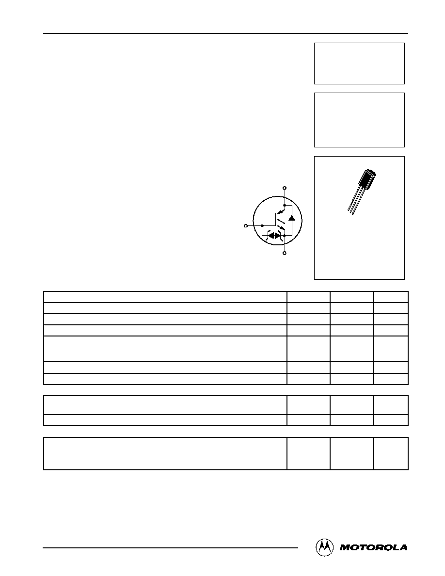
MGS05N60D
POWERLUX
IGBT
0.5 A @ 25
∞
C
600 V
CASE 029≠05
TO≠226AE
TO92 (1.0 WATT)
E
C
G
C
E
G
©
Motorola, Inc. 1997

MGS05N60D
2
Motorola Power Products Division Technical Data
ELECTRICAL CHARACTERISTICS
(TC = 25
∞
C unless otherwise noted)
Characteristic
Symbol
Min
Typ
Max
Unit
OFF CHARACTERISTICS
Collector≠to≠Emitter Breakdown Voltage
(VGE = 0 Vdc, IC = 250
µ
Adc)
Temperature Coefficient (Positive)
BVCES
600
--
680
0.7
--
--
Vdc
V/
∞
C
Zero Gate Voltage Collector Current
(VCE = 600 Vdc, VGE = 0 Vdc, TC = 25
∞
C)
(VCE = 600 Vdc, VGE = 0 Vdc, TC = 125
∞
C)
ICES
ICES
--
--
0.1
5.0
5.0
50
µ
Adc
Gate≠Body Leakage Current (VGE =
±
15 Vdc, VCE = 0 Vdc)
IGES
--
10
100
m
Adc
ON CHARACTERISTICS
Collector≠to≠Emitter On≠State Voltage
(VGE = 15 Vdc, IC = 0.3 Adc, TC = 25
∞
C)
(VGE = 15 Vdc, IC = 0.3 Adc, TC = 125
∞
C)
VCE(on)
--
--
1.6
1.5
2.0
--
Vdc
Gate Threshold Voltage
(VCE = VGE, IC = 250
m
Adc)
Threshold Temperature Coefficient (Negative)
VGE(th)
3.5
--
--
6.0
6.0
--
Vdc
mV/
∞
C
Forward Transconductance (VCE = 10 Vdc, IC = 0.5 Adc)
gfe
0.3
0.42
--
Mhos
DYNAMIC CHARACTERISTICS
Input Capacitance
(V
20 Vdc V
0 Vdc
Cies
--
75
100
pF
Output Capacitance
(VCE = 20 Vdc, VGE = 0 Vdc,
f = 1.0 MHz)
Coes
--
11
20
Transfer Capacitance
f = 1.0 MHz)
Cres
--
1.6
5.0
DIODE CHARACTERISTICS
Diode Forward Voltage Drop
(IEC = 0.3 Adc, TC = 25
∞
C)
(IEC = 0.3 Adc, TC = 125
∞
C)
(IEC = 0.1 Adc, TC = 25
∞
C)
(IEC = 0.1 Adc, TC = 125
∞
C)
VFEC
--
--
--
--
5.0
5.2
2.3
2.3
6.0
--
3.0
--
Vdc
Reverse Recovery Time @ TC = 25
∞
C
IF = 0.4 Adc, VR = 300 Vdc, dIF/dt = 10 A/
m
s
trr
--
150
--
ns
Reverse Recovery Stored Charge
IF = 0.4 Adc, VR = 300 Vdc, dIF/dt = 10 A/
m
s
QRR
--
35
--
m
C
SWITCHING CHARACTERISTICS (1)
Turn≠Off Delay Time
(VCC = 300 Vdc, IC = 0.4 Adc,
V
15 Vd
L
3 0
H R
25
td(off)
--
28
--
ns
Fall Time
VGE = 15 Vdc, L = 3.0 mH, RG = 25
,
TC = 25
∞
C, dV/dt = 1000 V/
m
s)
tf
--
150
--
Turn≠Off Switching Loss
TC = 25 C, dV/dt = 1000 V/
m
s)
Energy losses include "tail"
Eoff
--
3.25
4.25
m
J
Turn≠Off Delay Time
(VCC = 300 Vdc, IC = 0.4 Adc,
V
15 Vd
L
3 0
H R
25
td(off)
--
21
--
ns
Fall Time
VGE = 15 Vdc, L = 3.0 mH, RG = 25
,
TC = 125
∞
C, dV/dt = 1000 V/
m
s)
tf
--
280
--
Turn≠Off Switching Loss
TC = 125 C, dV/dt = 1000 V/
m
s)
Energy losses include "tail"
Eoff
--
8.0
10
m
J
Gate Charge
(VCC = 300 Vdc, IC = 0.3 Adc,
VGE = 15 Vdc)
QT
--
6.4
--
nC
(1) Pulse Test: Pulse Width
300
µ
s, Duty Cycle
2%.
MGS05N60D
3
Motorola Power Products Division Technical Data
Figure 1. Saturation Characteristics
Figure 2. Saturation Characteristics
Figure 3. Saturation Characteristics
Figure 4. Collector≠To≠Emitter Saturation
Voltage versus Case Temperature
Figure 5. Diode Forward Voltage
Figure 6. Diode Forward Voltage versus Case
Temperature
1.0
VCE, COLLECTOR≠TO≠EMITTER VOLTAGE (VOLTS)
2.5
2.0
1.5
1.0
VCE, COLLECTOR≠TO≠EMITTER VOLTAGE (VOLTS)
6.0
0
1.5
0.5
0
TC, CASE TEMPERATURE (
∞
C)
0
≠25
2.0
1.8
1.7
1.6
1.5
1.4
25
0.5
1.5
0
IF, COLLECTOR CURRENT (AMPS)
22
12
7.0
2.0
TC, CASE TEMPERATURE (
∞
C)
50
125
10
8.0
6.0
2.0
0
100
1.0
I CE
, COLLECT
OR≠EMITTER
CURRENT
(A)
V
CE
, COLLECT
OR≠T
O≠EMITTER VOL
T
AGE (V)
0.5
0
2.0
3.0
1.0
2.0
3.0
4.0
5.0
1.0
2.0
2.5
50
75
100
125
150
, EMITTER≠T
O≠COLLECT
OR VOL
T
AGE (V)
V
FEC
2.0
17
25
75
150
4.0
V
FEC
, COLLECT
OR≠T
O≠EMITTER VOL
T
AGE (V)
4.0
I C
, COLLECT
OR≠EMITTER
CURRENT
(A)
1.0
VCE, COLLECTOR≠TO≠EMITTER VOLTAGE (VOLTS)
2.5
2.0
1.5
1.0
I C
, COLLECT
OR≠EMITTER
CURRENT
(A)
0.5
0
2.0
3.0
4.0
1.9
TC = 25
∞
C
VGE = 15 V
12.5 V
10 V
8.0 V
TC = 150
∞
C
VGE = 15 V
12.5 V
10 V
8.0 V
TC = ≠20
∞
C
VGE = 15 V
12.5 V
10 V
8.0 V
IC = 700 m
VG = 15 V
IC = 500 mA
IC = 300 mA
TC = 150
∞
C
≠20
∞
C
25
∞
C
IC = 500 m
IC = 300 mA
IC = 100 mA

MGS05N60D
4
Motorola Power Products Division Technical Data
Figure 7. Capacitance Variation
Figure 8. Gate≠To≠Emitter Voltage versus
Total Charge
Figure 9. Total Switching Losses versus
Collector≠To≠Emitter Current
Figure 10. Total Switching Losses versus
Case Temperature
Figure 11. Minimum Turn≠Off
Safe Operating Area
20
25
0
COLLECTOR≠TO≠EMITTER VOLTAGE (VOLTS)
150
100
50
QG, TOTAL GATE CHARGE (nC)
6.0
0
10
5.0
0
2.0
0
IC, COLLECTOR≠TO≠EMITTER CURRENT (AMPS)
60
40
30
20
10
0
TC, CASE TEMPERATURE (
∞
C)
50
25
20
15
10
5.0
0
1.5
100
300
0
VCE, COLLECTOR≠TO≠EMITTER VOLTAGE (VOLTS)
2.5
2.0
1.5
1.0
0.5
0
200
C, CAP
ACIT
ANCE
(pF)
V
,
T
O
T
A
L
SWITCHING
ENERGY
LOSSES ( J)
0
10
5.0
15
7.0
1.0
2.0
3.0
4.0
5.0
15
m
0.5
1.0
75
100
150
, COLLECT
OR≠EMITTER
CURRENT
(A)
I CE
400
600
500
, GA
TE≠T
O≠EMITTER
VOL
T
AGE
(V)
GE
50
E
of
f
125
,
T
O
T
A
L
SWITCHING
ENERGY
LOSSES ( J)
m
E
of
f
VCE = 300 V
VGE = 15 V
IC = 0.3 A
TC = 25
∞
C
TC = 25
∞
C
Cies
Coes
Cres
L = 3.0 mH
VCC = 300 V
VGE = 15 V
RG = 25
W
dV/dt = 1.0 kV/
m
s
125
∞
C
25
∞
C
L = 3.0 mH
VCC = 300 V
VGE = 15 V
RG = 25
W
dV/dt = 1.0 kV/
m
s
0.7 A
0.3 A
TC = 125
∞
C
VGE = 15 V
RG = 25
W
L = 3.0 mH

MGS05N60D
5
Motorola Power Products Division Technical Data
t, TIME (ms)
r(t), TRANSIENT
THERMAL
RESIST
ANCE (NORMALIZED)
1.0
0.1
0.01
D = 0.5
SINGLE PULSE
1.0E≠05
1.0E≠04
1.0E≠03
1.0E≠02
1.0E≠01
1.0E+00
1.0E+01
0.2
0.1
0.05
0.02
0.01
1.0E+02
1.0E+03
0.001
R
JC(t) = r(t) R
JC
R
JC = 25
∞
C/W MAX
D CURVES APPLY FOR POWER
PULSE TRAIN SHOWN
READ TIME AT t1
TJ(pk) ≠ TC = P(pk) R
JC(t)
P(pk)
t1
t2
DUTY CYCLE, D = t1/t2
Figure 12. Typical Thermal Response
(R
q
JC(t))