MHVIC2115NR2
1
RF Device Data
Freescale Semiconductor
RF LDMOS Wideband Integrated
Power Amplifier
The MHVIC2115NR2 wideband integrated circuit is designed for base station
applications. It uses Freescale's newest High Voltage (26 to 28 Volts) LDMOS
IC technology and integrates a multi-stage structure. Its wideband On-Chip
matching design makes it usable from 1600 to 2600 MHz. The linearity
performances cover W-CDMA modulation formats.
Final Application
∑ Typical W-CDMA Performance: -45 dBc ACPR, 2110-2170 MHz, V
DD
=
27 Volts, I
DQ1
= 56 mA, I
DQ2
= 61 mA, I
DQ3
= 117 mA, P
out
= 34 dBm,
3GPP Test Model 1, Measured in 1.0 MHz BW @ 4 MHz offset, 64 DTCH
Power Gain -- 30 dB
PAE = 16%
Driver Application
∑ Typical W-CDMA Performance: -53 dBc ACPR, 2110-2170 MHz, V
DD
=
26 Volts, I
DQ1
= 96 mA, I
DQ2
= 204 mA, I
DQ3
= 111 mA, P
out
= 23 dBm,
3GPP Test Model 1, Measured in 3.84 MHz BW @ 5 MHz offset, 64 DTCH
Power Gain -- 34 dB
∑ Gain Flatness = 0.3 dB from 2110-2170 MHz
∑ P1dB = 15 Watts, Gain Flatness = 0.2 dB from 2110-2170 MHz
∑ Capable of Handling 3:1 VSWR, @ 26 Vdc, 2140 MHz, 15
Watts CW
Output Power
Features
∑ Characterized with Series Equivalent Large-Signal Impedance Parameters
∑ On-Chip Matching (50
Ohm Input, DC Blocked, >5 Ohm Output)
∑ Integrated Temperature Compensation with Enable/Disable Function
∑ Integrated ESD Protection
∑ RoHS Compliant
∑ In Tape and Reel. R2 Suffix = 1,500 Units per 16 mm, 13 inch Reel.
Table 1. Maximum Ratings
Rating
Symbol
Value
Unit
Drain-Source Voltage
V
DSS
-0.5, +65
Vdc
Gate-Source Voltage
V
GS
-0.5, +15
Vdc
Storage Temperature Range
T
stg
- 65 to +150
∞C
Operating Junction Temperature
T
J
150
∞C
16
15
14
13
12
11
10
1
2
3
4
5
6
7
8
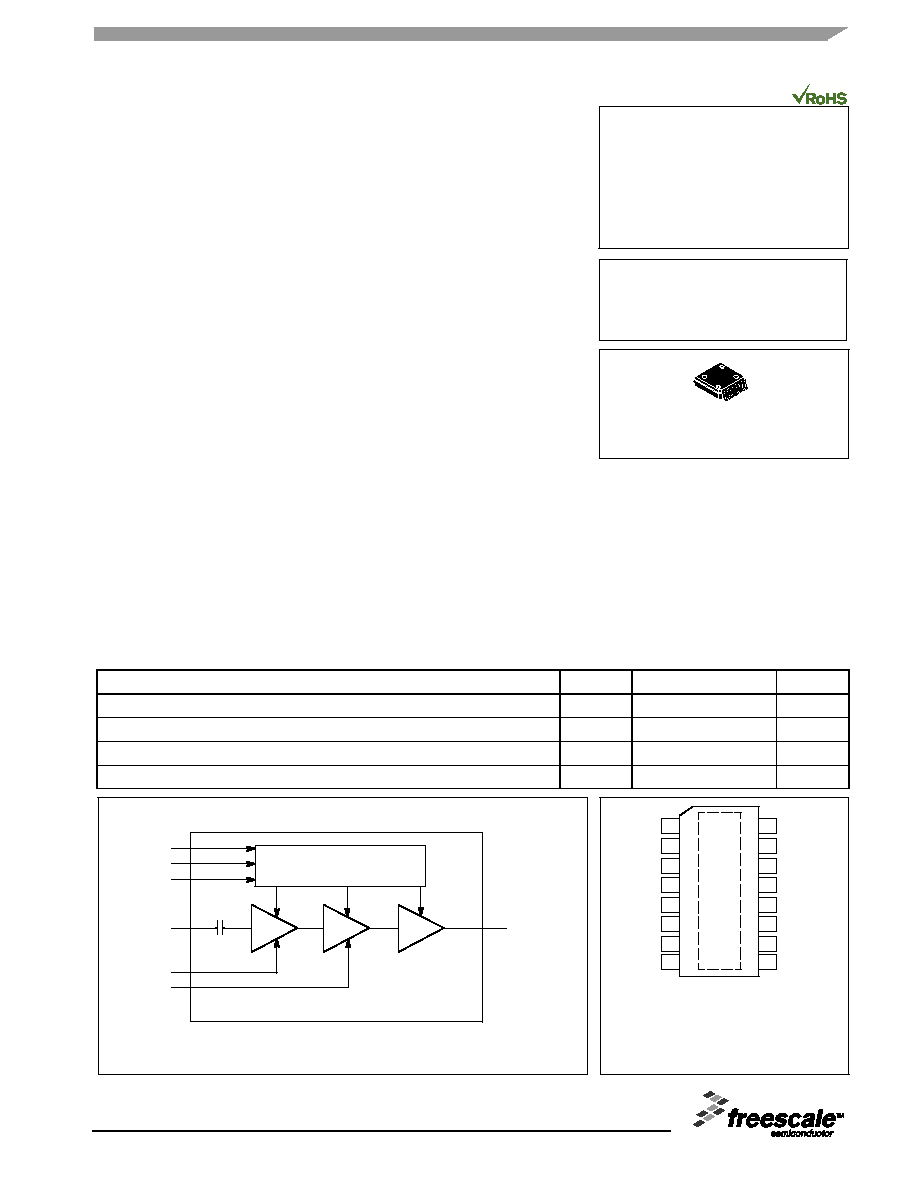
(Top View)
9
N.C.
V
GS3
V
GS2
V
GS1
RF
in
V
DS1
V
DS2
N.C.
V
DS3
/RF
out
V
DS3
/RF
out
V
DS3
/RF
out
V
DS3
/RF
out
V
DS3
/RF
out
V
DS3
/RF
out
N.C.
RF
in
Quiescent Current
Temperature Compensation
3 Stages I
C
V
DS1
RF
in
I
C
V
GS3
V
DS3
/RF
out
V
GS2
V
GS1
V
DS2
Note: Exposed backside flag is source
terminal for transistors.
Figure 1.
Block Diagram
Figure 2. Pin Connections
Document Number: MHVIC2115NR2
Rev. 5, 5/2006
Freescale Semiconductor
Technical Data
MHVIC2115NR2
CASE 978-03
PFP-16
2170 MHz, 26 V, 23/34 dBm
W-CDMA
RF LDMOS WIDEBAND
INTEGRATED POWER AMPLIFIER
16
1
© Freescale Semiconductor, Inc., 2006. All rights reserved.
2
RF Device Data
Freescale Semiconductor
MHVIC2115NR2
Table 2. Thermal Characteristics
Characteristic
Symbol
Value
Unit
Thermal Resistance, Junction to Case
Driver Application
Stage 1, 26 Vdc, I
DQ
= 96 mA
(P
out
= +0.2 W CW)
Stage 2, 26 Vdc, I
DQ
= 204 mA
Stage 3, 26 Vdc, I
DQ
= 111 mA
Output Application
Stage 1, 27 Vdc, I
DQ
= 56 mA
(P
out
= +2.5 W CW)
Stage 2, 27 Vdc, I
DQ
= 61 mA
Stage 3, 27 Vdc, I
DQ
= 117 mA
R
JC
3.5
2.7
∞C/W
Table 3. ESD Protection Characteristics
Test Conditions
Class
Human Body Model
1 (Minimum)
Machine Model
M1 (Minimum)
Charge Device Model
C2 (Minimum)
Table 4. Moisture Sensitivity Level
Test Methodology
Rating
Package Peak Temperature
Unit
Per JESD 22-A113, IPC/JEDEC J-STD-020
3
260
∞C
Table 5. Electrical Characteristics
(T
C
= 25∞C unless otherwise noted)
Characteristic
Symbol
Min
Typ
Max
Unit
W-CDMA Characteristics (In Freescale Test Fixture, 50 ohm system) V
DD
= 26 Vdc, I
DQ1
= 96 mA, I
DQ2
= 204 mA, I
DQ3
= 111 mA,
P
out
= 23 dBm, 2110-2170 MHz
Power Gain
G
ps
31
34
--
dB
Gain Flatness
G
F
--
0.3
0.5
dB
Input Return Loss
IRL
--
-12
-10
dB
Group Delay
--
--
1.7
--
ns
Phase Linearity
--
--
0.2
--
∞
1-Carrier W-CDMA Conditions: Adjacent Channel Power Ratio
@ P
out
= 23 dBm, 5 MHz Offset
ACPR
--
-53
-50
dBc
1-Carrier W-CDMA Conditions: Adjacent Channel Power Ratio
@ P
out
= 28 dBm, 5 MHz Offset
ACPR
--
-50
--
dBc
W-CDMA Characteristics (In Freescale Test Fixture, 50 ohm system) V
DD
= 27 Vdc, I
DQ1
= 56 mA, I
DQ2
= 61 mA, I
DQ3
= 117 mA,
P
out
= 34 dBm, 2110-2170 MHz
Power Gain
G
ps
--
30
--
dB
Gain Flatness
G
F
--
0.2
--
dB
Input Return Loss
IRL
--
-12
--
dB
Power Added Efficiency
PAE
--
16
--
%
1-Carrier W-CDMA Conditions: Adjacent Channel Power Ratio
@ P
out
= 34 dBm, 4 MHz Offset
ACPR
--
-45
--
dBc

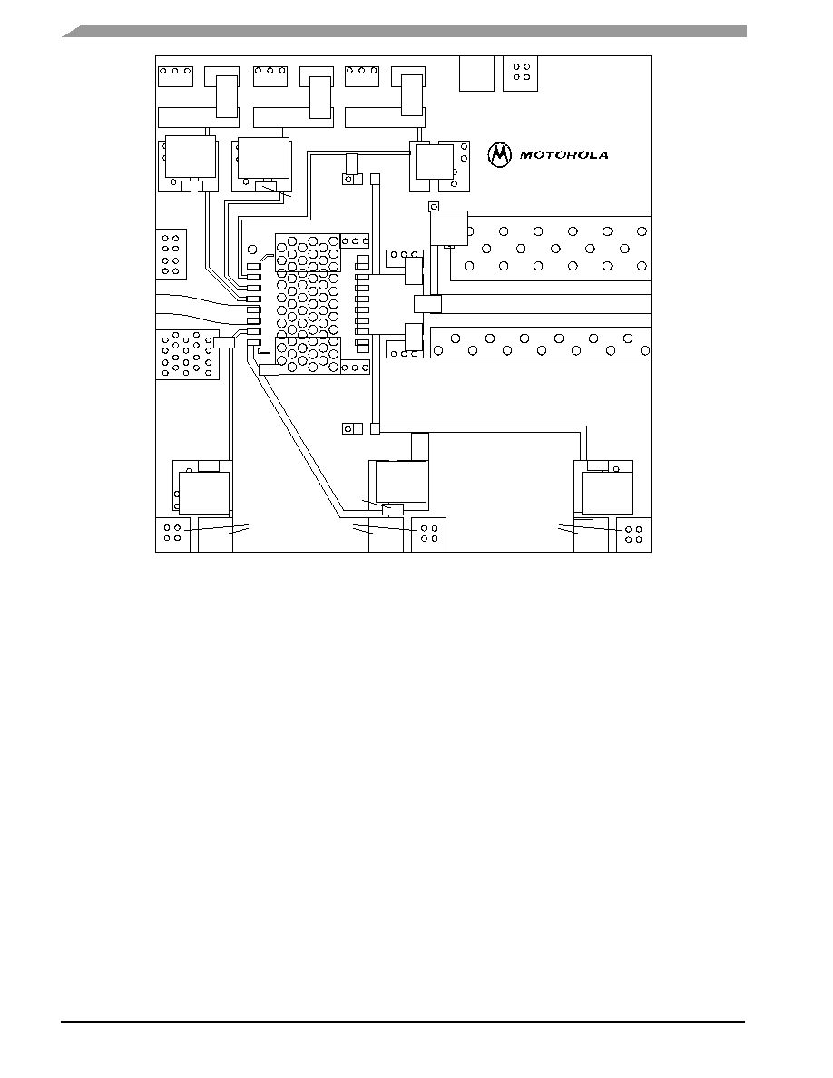
MHVIC2115NR2
3
RF Device Data
Freescale Semiconductor
C1, C5, C8, C12, C14, C19 1 mF SMT Tantalum Chip Capacitors
C2, C3, C4, C7, C11, C18
0.01 mF Chip Capacitors (0805C103K5RACTR)
C6, C10, C17
6.8 pF Chip Capacitors, ACCU-P (AVX 08051J6R8BBT)
C9, C15, C16
1.8 pF Chip Capacitors, ACCU-P (AVX 08051J1R8BBT)
C13, C20, C21 330 mF Electrolytic Capacitors
(MCR35V337M10X16)
R1, R2, R3
1 kW Chip Resistors (0805)
PCB
Arlon, 0.020,, e
r
= 2.55
Figure 3. MHVIC2115NR2 Demo Board Schematic
C19
RF
OUTPUT
C9
C15
16
15
14
13
12
11
10
9
1
2
3
4
5
6
7
8
C16
C17
V
D3
C20
C18
V
D2
C13
V
D1
RF
INPUT
R3
C2
C1
V
bias3
R1
C4
C14
V
bias1
R2
C3
C5
V
bias2
+
C8
+
C7
C6
C12
+
C11
C10
C21
+
+
+
+
+
+
Quiescent Current
Temperature Compensation
4
RF Device Data
Freescale Semiconductor
MHVIC2115NR2
Rev 1
MHVIC2115R2
V
DD3
C7
V
DD2
V
DD1
R1
R2
R3
C1
C2
C3
C4
C6
C5
C10
C9
C11
C14
C15
C16
C13
C18
C20
C17
C21
V
GS
Figure 4. MHVIC2115NR2 Demo Board Component Layout
C19
C12
C8
V
G1
V
G2
V
G3
V
bias1
V
bias2
V
bias3
Freescale has begun the transition of marking Printed Circuit Boards (PCBs) with the Freescale Semiconductor
signature/logo. PCBs may have either Motorola or Freescale markings during the transition period. These changes will have
no impact on form, fit or function of the current product.

MHVIC2115NR2
5
RF Device Data
Freescale Semiconductor
TYPICAL CHARACTERISTICS
3000
-20
50
1000
-35
0
S21
f, FEQUENCY (MHz)
Figure 5. Broadband Frequency Response
S21 (dB)
S1
1 (dB)
S11
40
-5
30
-10
20
-15
10
-20
0
-25
-10
-30
2800
2600
2400
2200
2000
1800
1600
1400
1200
V
DD
= 27 Vdc, P
out
= 23 dBm CW
I
DQ1
= 96 mA, I
DQ2
= 204 mA, I
DQ3
= 111 mA
2180
0
1.8
2100
f, FREQUENCY (MHz)
Figure 6. Delay versus Frequency
DELA
Y
, (nSEC)
T
C
= 85
_C
1.6
1.4
1.2
1
0.8
0.6
0.4
0.2
2110
2120
2130
2140
2150
2160
2170
V
DD
= 27 Vdc, P
out
= 23 dBm CW
I
DQ1
= 96 mA, I
DQ2
= 204 mA, I
DQ3
= 111 mA
25
_C
-30
_C
2180
2100
2110
2120
2130
2140
2150
2160
2170
30
40
f, FREQUENCY (MHz)
Figure 7. Power Gain versus Frequency
G
ps
, POWER GAIN (dB)
39
38
37
36
35
34
33
32
31
25
_C
85
_C
V
DD
= 27 Vdc, P
out
= 23 dBm CW
I
DQ1
= 96 mA, I
DQ2
= 204 mA, I
DQ3
= 111 mA
T
C
= -30
_C
2180
2100
2110
2120
2130
2140
2150
2160
2170
0
20
f, FREQUENCY, (MHz)
Figure 8. Input Return Loss versus Frequency
INPUT
RETURN LOSS (dB)
IRL,
15
10
5
V
DD
= 27 Vdc, P
out
= 23 dBm CW
I
DQ1
= 96 mA, I
DQ2
= 204 mA, I
DQ3
= 111 mA
25
_C
-30
_C
T
C
= 85
_C
30
40
20
P
out
, OUTPUT POWER (dBm)
Figure 9. Power Gain versus Output Power
G
ps
, POWER GAIN (dB)
25
_C
85
_C
T
C
= -30
_C
25
30
35
40
45
39
38
37
36
35
34
33
32
31
40
70
20
-30
_C
85
_C
T
C
= 25
_C
25
30
35
40
45
65
60
55
50
45
P
out
, OUTPUT POWER (dBm)
Figure 10. S21 Phase versus Output Power
S21 PHASE(
_
)
V
DD
= 27 Vdc, f = 2140 MHz
I
DQ1
= 96 mA, I
DQ2
= 204 mA, I
DQ3
= 111 mA
V
DD
= 27 Vdc, f = 2140 MHz
I
DQ1
= 96 mA, I
DQ2
= 204 mA, I
DQ3
= 111 mA