 | ÐлекÑÑоннÑй компоненÑ: MPS6601 | СкаÑаÑÑ:  PDF PDF  ZIP ZIP |
Äîêóìåíòàöèÿ è îïèñàíèÿ www.docs.chipfind.ru
1
Motorola SmallSignal Transistors, FETs and Diodes Device Data
Amplifier Transistors
MAXIMUM RATINGS
Rating
Symbol
Value
Unit
Collector Emitter Voltage
MPS6601/6651
MPS6602/6652
VCEO
25
40
Vdc
Collector Base Voltage
MPS6601/6651
MPS6602/6652
VCBO
25
30
Vdc
Emitter Base Voltage
VEBO
4.0
Vdc
Collector Current -- Continuous
IC
1000
mAdc
Total Device Dissipation @ TA = 25
°
C
Derate above 25
°
C
PD
625
5.0
mW
mW/
°
C
Total Device Dissipation @ TC = 25
°
C
Derate above 25
°
C
PD
1.5
12
Watts
mW/
°
C
Operating and Storage Junction
Temperature Range
TJ, Tstg
55 to
+150
°
C
THERMAL CHARACTERISTICS
Characteristic
Symbol
Max
Unit
Thermal Resistance, Junction to Ambient
R
q
JA
(1)
200
°
C/W
Thermal Resistance, Junction to Case
R
q
JC
83.3
°
C/W
ELECTRICAL CHARACTERISTICS
(TA = 25
°
C unless otherwise noted)
Characteristic
Symbol
Min
Max
Unit
OFF CHARACTERISTICS
Collector Emitter Breakdown Voltage
(IC = 1.0 mAdc, IB = 0)
MPS6601/6651
MPS6602/6652
V(BR)CEO
25
40
--
--
Vdc
Collector Base Breakdown Voltage
(IC = 100
µ
Adc, IE = 0)
MPS6601/6651
MPS6602/6652
V(BR)CBO
25
40
--
--
Vdc
Emitter Base Breakdown Voltage
(IE = 10
µ
Adc, IC = 0)
V(BR)EBO
4.0
--
Vdc
Collector Cutoff Current
(VCE = 25 Vdc, IB = 0)
MPS6601/6651
(VCE = 30 Vdc, IB = 0)
MPS6602/6652
ICES
--
--
0.1
0.1
µ
Adc
Collector Cutoff Current
(VCB = 25 Vdc, IE = 0)
MPS6601/6651
(VCB = 30 Vdc, IE = 0)
MPS6602/6652
ICBO
--
--
0.1
0.1
µ
Adc
1. R
q
JA is measured with the device soldered into a typical printed circuit board.
Preferred devices are Motorola recommended choices for future use and best overall value.
Order this document
by MPS6601/D
MOTOROLA
SEMICONDUCTOR TECHNICAL DATA
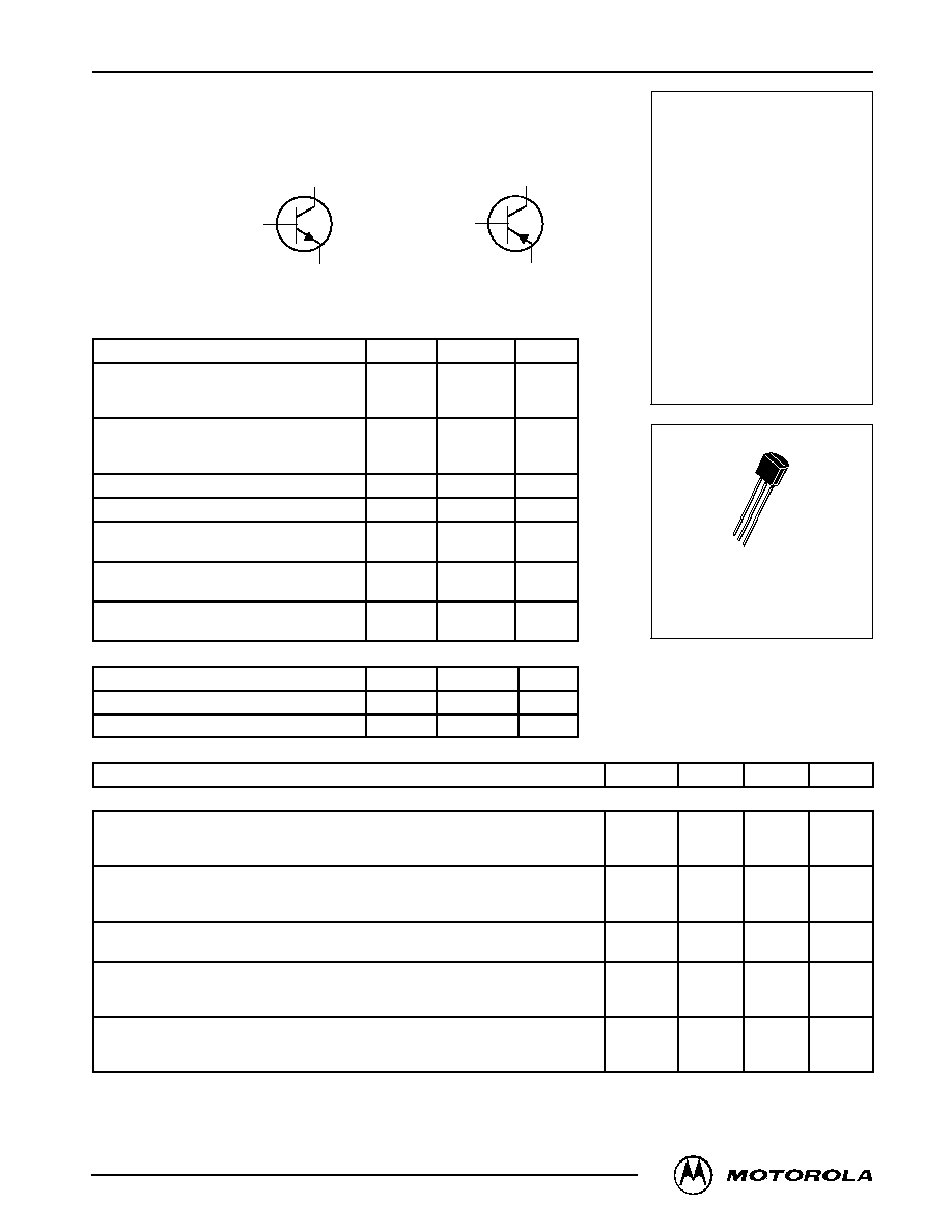
NPN
MPS6601
MPS6602
PNP
MPS6651
MPS6652
*Motorola Preferred Device
*
CASE 2904, STYLE 1
TO92 (TO226AA)
1
2
3
*
Voltage and current are negative
for PNP transistors
©
Motorola, Inc. 1996
COLLECTOR
3
2
BASE
1
EMITTER
COLLECTOR
3
2
BASE
1
EMITTER
NPN
PNP
NPN MPS6601 MPS6602 PNP MPS6651 MPS6652
2
Motorola SmallSignal Transistors, FETs and Diodes Device Data
ELECTRICAL CHARACTERISTICS
(TA = 25
°
C unless otherwise noted) (Continued)
Characteristic
Symbol
Min
Max
Unit
ON CHARACTERISTICS
DC Current Gain
(IC = 100 mAdc, VCE = 1.0 Vdc)
(IC = 500 mAdc, VCE = 1.0 Vdc)
(IC = 1000 mAdc, VCE = 1.0 Vdc)
hFE
50
50
30
--
--
--
--
Collector Emitter Saturation Voltage
(IC = 1000 mAdc, IB = 100 mAdc)
VCE(sat)
--
0.6
Vdc
BaseEmitter On Voltage
(IC = 500 mAdc, VCE = 1.0 Vdc)
VBE(on)
--
1.2
Vdc
SMALL SIGNAL CHARACTERISTICS
Current Gain -- Bandwidth Product
(IC = 50 mAdc, VCE = 10 Vdc, f = 100 MHz)
fT
100
--
MHz
Output Capacitance
(VCB = 10 Vdc, IE = 0, f = 1.0 MHz)
Cobo
--
30
pF
SWITCHING CHARACTERISTICS
Delay Time
(VCC = 40 Vdc, IC = 500 mAdc,
IB1 = 50 mAdc,
tp
w
300 ns Duty Cycle)
td
--
25
ns
Rise Time
(VCC = 40 Vdc, IC = 500 mAdc,
IB1 = 50 mAdc,
tp
w
300 ns Duty Cycle)
tr
--
30
ns
Storage Time
IB1 = 50 mAdc,
tp
w
300 ns Duty Cycle)
ts
--
250
ns
Fall Time
p
w
300 ns Duty Cycle)
tf
--
50
ns
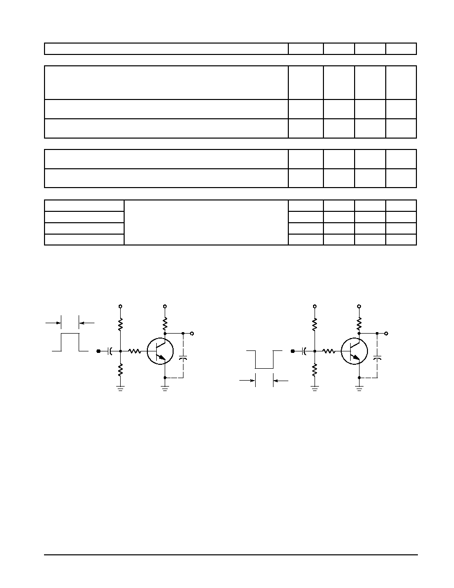
Figure 1. Switching Time Test Circuits
OUTPUT
TURNON TIME
1.0 V
VCC
+40
V
RL
* CS
t
6.0 pF
RB
100
100
Vin
5.0
m
F
tr = 3.0 ns
0
+10
V
5.0
m
s
OUTPUT
TURNOFF TIME
+VBB
VCC
+40
V
RL
* CS
t
6.0 pF
RB
100
100
Vin
5.0
m
F
tr = 3.0 ns
5.0
m
s
* Total Shunt Capacitance of Test Jig and Connectors
For PNP Test Circuits, Reverse All Voltage Polarities
NPN MPS6601 MPS6602 PNP MPS6651 MPS6652
3
Motorola SmallSignal Transistors, FETs and Diodes Device Data
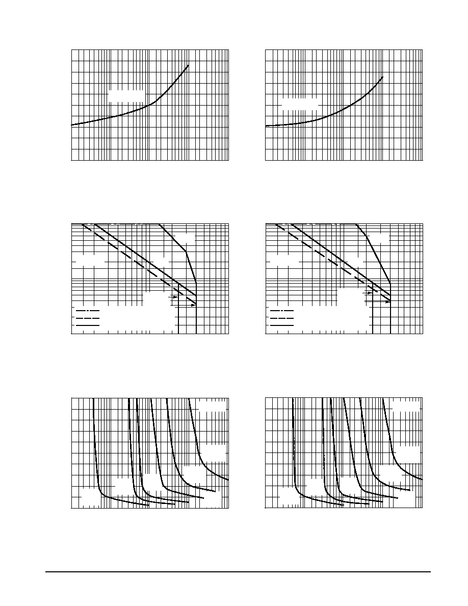
Figure 2. MPS6601/6602 DC Current Gain
Figure 3. MPS6651/6652 DC Current Gain
Figure 4. Current Gain Bandwidth Product
Figure 5. Current Gain Bandwidth Product
Figure 6. On Voltages
Figure 7. On Voltages
100
1000
10
IC, COLLECTOR CURRENT (mA)
300
200
100
70
50
30
IC, COLLECTOR CURRENT (mA)
100
1000
10
200
100
70
50
20
100
1000
10
IC, COLLECTOR CURRENT (mA)
300
200
100
70
50
30
IC, COLLECTOR CURRENT (mA)
100
1000
10
300
200
100
70
50
30
200
200
10
1000
1.0
IC, COLLECTOR CURRENT (mA)
1.0
0.8
0.6
0.4
0.2
0
IC, COLLECTOR CURRENT (mA)
10
1000
1.0
1.0
0.8
0.6
0.4
0.2
0
100
100
TJ = 25
°
C
TJ = 25
°
C
VCE = 1.0 V
TJ = 25
°
C
VCE = 1.0 V
TJ = 25
°
C
VCE = 10 V
TJ = 25
°
C
f = 30 MHz
VCE = 10 V
TJ = 25
°
C
f = 30 MHz
f T
, CURRENT
GAIN BANDWIDTH PRODUCT
(MHz)
V
, VOL
T
AGE (VOL
TS)
V
, VOL
T
AGE (VOL
TS)
NPN
PNP
VBE(SAT) @ IC/IB = 10
VCE(SAT) @ IC/IB = 10
VBE(ON) @ VCE = 1.0 V
VBE(SAT) @ IC/IB = 10
VCE(SAT) @ IC/IB = 10
VBE(ON) @ VCE = 1.0 V
f T
, CURRENT
GAIN BANDWIDTH PRODUCT
(MHz)
FE
h , CURRENT
GAIN
h , CURRENT
GAIN
FE
NPN MPS6601 MPS6602 PNP MPS6651 MPS6652
4
Motorola SmallSignal Transistors, FETs and Diodes Device Data
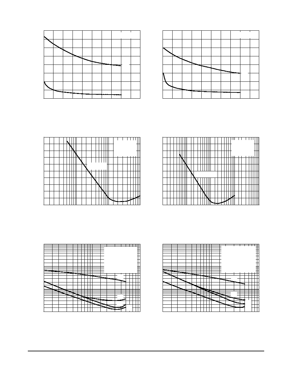
Figure 8. Capacitance
Figure 9. Capacitance
Figure 10. MPS6601/6602 Noise Figure
Figure 11. MPS6651/6652 Noise Figure
Figure 12. MPS6601/6602 Switching Times
Figure 13. MPS6651/6652 Switching Times
10
25
Cob
VR, REVERSE VOLTAGE (VOLTS)
80
60
40
20
0
VR, REVERSE VOLTAGE (VOLTS)
160
120
80
40
0
100
10 k
10
Rs, SOURCE RESISTANCE (OHMS)
10
8.0
6.0
4.0
2.0
0
Rs, SOURCE RESISTANCE (OHMS)
1 k
10
10
8.0
6.0
4.0
2.0
0
10 k
1 k
20
1000
10
IC, COLLECTOR CURRENT (mA)
200
100
50
20
10
IC, COLLECTOR CURRENT (mA)
20
1000
10
500
200
100
50
20
10
100
100
TJ = 25
°
C
VCE = 5.0 V
f = 1.0 kHz
TA = 25
°
C
C, CAP
ACIT
ANCE (pF)
NF
, NOISE FIGURE (dB)
NF
, NOISE FIGURE (dB)
t,
TIME (NS)
t,
TIME (NS)
NPN
PNP
5.0
15
20
2.0
5.0
Cib
1.0
3.0
4.0
10
25
Cob
5.0
15
20
Cib
2.0
5.0
1.0
3.0
4.0
TJ = 25
°
C
C, CAP
ACIT
ANCE (pF)
IC = 100
m
A
100
VCE = 5.0 V
f = 1.0 kHz
TA = 25
°
C
IC = 100
m
A
50
200
500
1 k
500
3 k
10 k
5 k
td @ VBE(off) = 0.5 V
VCC = 40 V
IC/IB = 10
IB1 = IB2
TJ = 25
°
C
ts
tf
tr
td
td @ VBE(off) = 0.5 V
VCC = 40 V
IC/IB = 10
IB1 = IB2
TJ = 25
°
C
ts
tf
tr
td
50
200
500
1 k
3 k
5 k
10 k
Cib
Cob
Cib
Cob
NPN MPS6601 MPS6602 PNP MPS6651 MPS6652
5
Motorola SmallSignal Transistors, FETs and Diodes Device Data
Figure 14. BaseEmitter Temperature
Coefficient
Figure 15. BaseEmitter Temperature
Coefficient
Figure 16. Safe Operating Area
Figure 17. Safe Operating Area
Figure 18. MPS6601/6602 Saturation Region
Figure 19. MPS6651/6652 Saturation Region
100
1000
1.0
IC, COLLECTOR CURRENT (mA)
0.8
1.2
1.6
2.0
2.4
2.8
IC, COLLECTOR CURRENT (mA)
100
1000
1.0
1.2
1.6
2.0
2.4
2.8
10
1.0
VCE, COLLECTOREMITTER VOLTAGE
500
200
100
50
20
10
VCE, COLLECTOREMITTER VOLTAGE
10
40
1.0
500
200
100
50
20
10
20
20
0.1
10
0.01
IB, BASE CURRENT (mA)
1.0
0.8
0.6
0.4
0.2
0
IB, BASE CURRENT (mA)
0.1
100
0.01
1.0
0.8
0.6
0.4
0.2
0
1.0
1.0
TJ = 25
°
C
R
VB
,
TEMPERA
TURE COEFFICIENT
(mV/ C)
I C
, COLLECT
OR CURRENT
(mA)
NPN
PNP
10
R
q
VB for VBE
q
°
R
VB
,
TEMPERA
TURE COEFFICIENT
(mV/ C)
q
°
10
0.8
R
q
VB for VBE
2.0
5.0
1 k
2.0
5.0
40
1 k
I C
, COLLECT
OR CURRENT
(mA)
10
100
IC =
100 mA
IC =
50 mA
IC =
250 mA
IC =
500 mA
IC =
1000 mA
IC =
10 mA
TJ = 25
°
C
IC =
100 mA
IC =
50 mA
IC =
250 mA
IC =
500 mA
IC =
1000 mA
IC =
10 mA
1.0 MS
1.0 s
TC = 25
°
C
MPS6601
CURRENT LIMIT
THERMAL LIMIT
SECOND BREAKDOWN LIMIT
MPS6602
1.0 MS
1.0 s
TC = 25
°
C
MPS6651
CURRENT LIMIT
THERMAL LIMIT
SECOND BREAKDOWN LIMIT
MPS6652
, COLLECT
OR VOL
T
AGE (VOL
TS)
V
CE
, COLLECT
OR VOL
T
AGE (VOL
TS)
V
CE
NPN MPS6601 MPS6602 PNP MPS6651 MPS6652
6
Motorola SmallSignal Transistors, FETs and Diodes Device Data
Figure 20. Thermal Response
t, TIME (SECONDS)
0.001
0.002
0.005
0.01
0.02
0.05
0.1
0.2
0.5
1.0
2.0
5.0
10
20
50
100
0.03
0.02
0.1
0.07
0.05
0.01
0.3
0.2
1.0
0.7
0.5
r(t), NORMALIZED EFFECTIVE
TRANSIENT
THERMAL
RESIST
ANCE
R
JC(t) = (t)
JC
R
JC = 100
°
C/W MAX
R
JA(t)d = r(t)
JA
R
JA = 357
°
C/W MAX
D CURVES APPLY FOR
POWER PULSE TRAIN
SHOWN READ TIME AT t1
TJ(pk) TC = P(pk)
JC(t)
t1
t2
DUTY CYCLE, D = t1/t2
P(pk)
D = 0.5
0.2
0.1
0.05
0.02
0.01
SINGLE PULSE
SINGLE PULSE
NPN MPS6601 MPS6602 PNP MPS6651 MPS6652
7
Motorola SmallSignal Transistors, FETs and Diodes Device Data
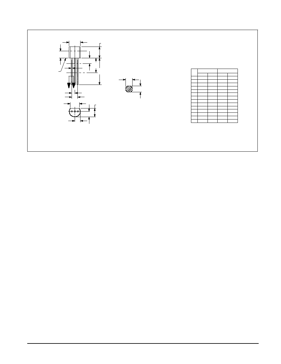
PACKAGE DIMENSIONS
NOTES:
1. DIMENSIONING AND TOLERANCING PER ANSI
Y14.5M, 1982.
2. CONTROLLING DIMENSION: INCH.
3. CONTOUR OF PACKAGE BEYOND DIMENSION R
IS UNCONTROLLED.
4. DIMENSION F APPLIES BETWEEN P AND L.
DIMENSION D AND J APPLY BETWEEN L AND K
MINIMUM. LEAD DIMENSION IS UNCONTROLLED
IN P AND BEYOND DIMENSION K MINIMUM.
R
A
P
J
L
F
B
K
G
H
SECTION XX
C
V
D
N
N
X X
SEATING
PLANE
DIM
MIN
MAX
MIN
MAX
MILLIMETERS
INCHES
A
0.175
0.205
4.45
5.20
B
0.170
0.210
4.32
5.33
C
0.125
0.165
3.18
4.19
D
0.016
0.022
0.41
0.55
F
0.016
0.019
0.41
0.48
G
0.045
0.055
1.15
1.39
H
0.095
0.105
2.42
2.66
J
0.015
0.020
0.39
0.50
K
0.500
12.70
L
0.250
6.35
N
0.080
0.105
2.04
2.66
P
0.100
2.54
R
0.115
2.93
V
0.135
3.43
1
STYLE 1:
PIN 1. EMITTER
2. BASE
3. COLLECTOR
CASE 02904
(TO226AA)
ISSUE AD

NPN MPS6601 MPS6602 PNP MPS6651 MPS6652
8
Motorola SmallSignal Transistors, FETs and Diodes Device Data
Motorola reserves the right to make changes without further notice to any products herein. Motorola makes no warranty, representation or guarantee regarding
the suitability of its products for any particular purpose, nor does Motorola assume any liability arising out of the application or use of any product or circuit, and
specifically disclaims any and all liability, including without limitation consequential or incidental damages. "Typical" parameters which may be provided in Motorola
data sheets and/or specifications can and do vary in different applications and actual performance may vary over time. All operating parameters, including "Typicals"
must be validated for each customer application by customer's technical experts. Motorola does not convey any license under its patent rights nor the rights of
others. Motorola products are not designed, intended, or authorized for use as components in systems intended for surgical implant into the body, or other
applications intended to support or sustain life, or for any other application in which the failure of the Motorola product could create a situation where personal injury
or death may occur. Should Buyer purchase or use Motorola products for any such unintended or unauthorized application, Buyer shall indemnify and hold Motorola
and its officers, employees, subsidiaries, affiliates, and distributors harmless against all claims, costs, damages, and expenses, and reasonable attorney fees
arising out of, directly or indirectly, any claim of personal injury or death associated with such unintended or unauthorized use, even if such claim alleges that
Motorola was negligent regarding the design or manufacture of the part. Motorola and are registered trademarks of Motorola, Inc. Motorola, Inc. is an Equal
Opportunity/Affirmative Action Employer.
How to reach us:
USA / EUROPE / Locations Not Listed: Motorola Literature Distribution;
JAPAN: Nippon Motorola Ltd.; TatsumiSPDJLDC, 6F SeibuButsuryuCenter,
P.O. Box 20912; Phoenix, Arizona 85036. 18004412447 or 6023035454
3142 Tatsumi KotoKu, Tokyo 135, Japan. 038135218315
MFAX: RMFAX0@email.sps.mot.com TOUCHTONE 6022446609
ASIA/PACIFIC: Motorola Semiconductors H.K. Ltd.; 8B Tai Ping Industrial Park,
INTERNET: http://DesignNET.com
51 Ting Kok Road, Tai Po, N.T., Hong Kong. 85226629298
MPS6601/D
*MPS6601/D*