 | –≠–ª–µ–∫—Ç—Ä–æ–Ω–Ω—ã–π –∫–æ–º–ø–æ–Ω–µ–Ω—Ç: MRF1150MA | –°–∫–∞—á–∞—Ç—å:  PDF PDF  ZIP ZIP |
1
MRF1150MA MRF1150MB
MOTOROLA RF DEVICE DATA
The RF Line
Microwave Pulse
Power Transistors
Designed for Class B and C common base amplifier applications in short
pulse TACAN, IFF, and DME transmitters.
∑
Guaranteed Performance @ 1090 MHz, 50 Vdc
Output Power = 150 Watts Peak
Minimum Gain = 7.8 dB
∑
100% Tested for Load Mismatch at All Phase Angles with 10:1 VSWR
∑
Industry Standard Package
∑
Nitride Passivated
∑
Gold Metallized, Emitter Ballasted for Long Life and Resistance to Metal
Migration
∑
Internal Input Matching for Broadband Operation
∑
Circuit board photomaster available upon request by contacting
RF Tactical Marketing in Phoenix, AZ.
MAXIMUM RATINGS
Rating
Symbol
Value
Unit
Collector≠Base Voltage
VCBO
70
Vdc
Emitter≠Base Voltage
VEBO
4.0
Vdc
Collector Current -- Peak (1)
IC
12
Adc
Total Device Dissipation @ TC = 25
∞
C (1) (2)
Derate above 25
∞
C
PD
583
3.33
Watts
W/
∞
C
Storage Temperature Range
Tstg
≠ 65 to +150
∞
C
THERMAL CHARACTERISTICS
Characteristic
Symbol
Max
Unit
Thermal Resistance, Junction to Case (3)
R
JC
0.3
∞
C/W
ELECTRICAL CHARACTERISTICS
(TC = 25
∞
C unless otherwise noted)
Characteristic
Symbol
Min
Typ
Max
Unit
OFF CHARACTERISTICS
Collector≠Emitter Breakdown Voltage
(IC = 50 mAdc, VBE = 0)
V(BR)CES
70
--
--
Vdc
Collector≠Base Breakdown Voltage
(IC = 50 mAdc, IE = 0)
V(BR)CBO
70
--
--
Vdc
Emitter≠Base Breakdown Voltage
(IE = 5.0 mAdc, IC = 0)
V(BR)EBO
4.0
--
--
Vdc
Collector Cutoff Current
(VCB = 50 Vdc, IE = 0)
ICBO
--
--
10
mAdc
ON CHARACTERISTICS
DC Current Gain (4)
(IC = 5.0 Adc, VCE = 5.0 Vdc)
hFE
10
30
--
--
NOTES:
(continued)
1. Pulse Width = 10
µ
s, Duty Cycle = 1%.
2. These devices are designed for RF operation. The total device dissipation rating applies only when the device is operated as RF amplifiers.
3. Thermal Resistance is determined under specified RF operating conditions by infrared measurement techniques.
4. 80
µ
s Pulse on Tektronix 576 or equivalent.
Order this document
by MRF1150MA/D
MOTOROLA
SEMICONDUCTOR TECHNICAL DATA
MRF1150MA
MRF1150MB
150 W PEAK, 960 ≠ 1215 MHz
MICROWAVE POWER
TRANSISTORS
NPN SILICON
CASE 332≠04, STYLE 1
(MRF1150MA)
CASE 332A≠03, STYLE 1
(MRF1150MB)
©
Motorola, Inc. 1997
REV 8
MRF1150MA MRF1150MB
2
MOTOROLA RF DEVICE DATA
ELECTRICAL CHARACTERISTICS -- continued
(TC = 25
∞
C unless otherwise noted)
Characteristic
Symbol
Min
Typ
Max
Unit
DYNAMIC CHARACTERISTICS
Output Capacitance
(VCB = 50 Vdc, IE = 0, f = 1.0 MHz)
Cob
--
25
32
pF
FUNCTIONAL TESTS
(Pulse Width = 10
µ
s, Duty Cycle = 1.0%)
Common≠Base Amplifier Power Gain
(VCC = 50 Vdc, Pout = 150 W pk, f = 1090 MHz)
GPB
7.8
9.8
--
dB
Collector Efficiency
(VCC = 50 Vdc, Pout = 150 W pk, f = 1090 MHz)
35
40
--
%
Load Mismatch
(VCC = 50 Vdc, Pout = 150 W pk, f = 1090 MHz,
VSWR = 10:1 All Phase Angles)
No Degradation in Power Output
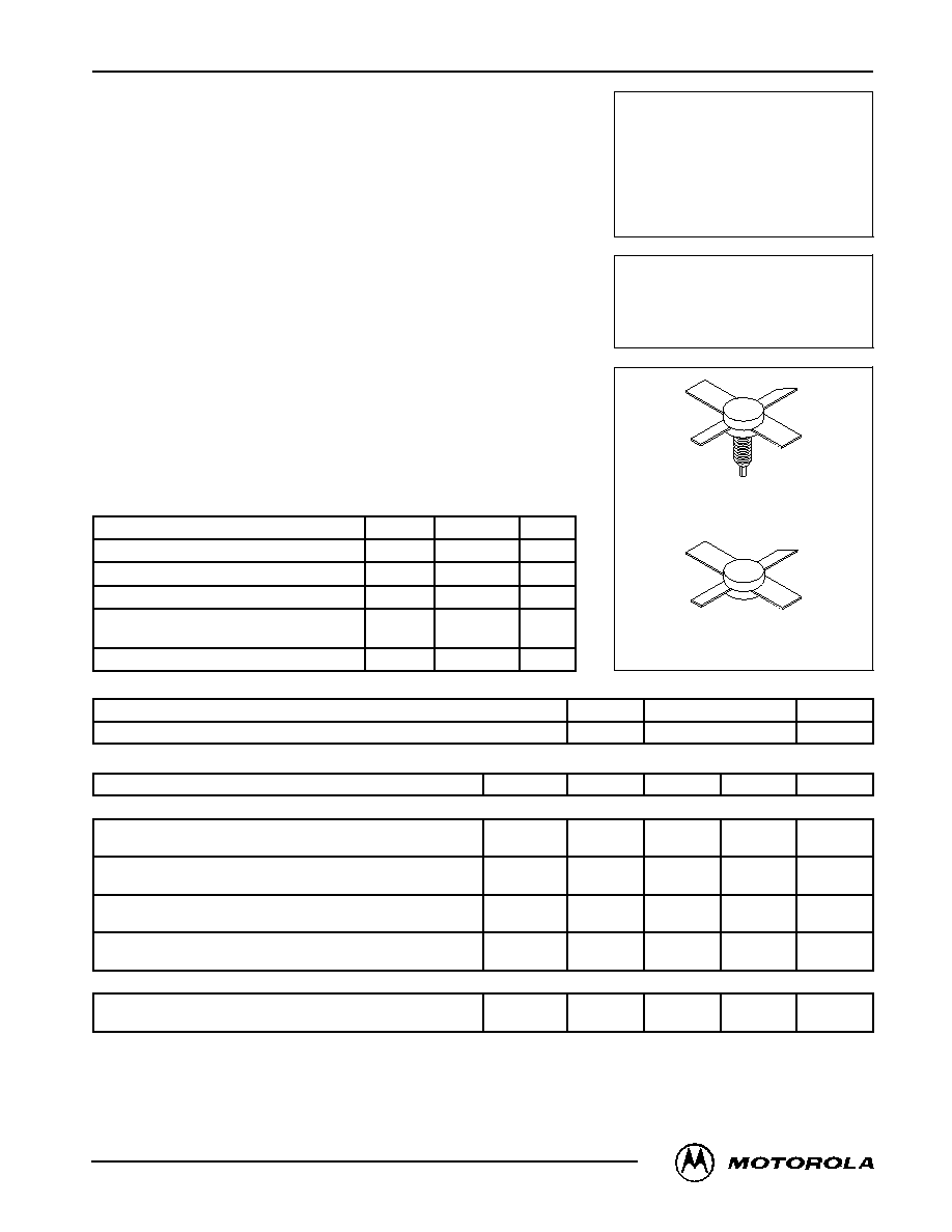
Figure 1. 1090 MHz Test Circuit
C1, C2 -- 220 pF Chip Capacitor, 100≠mil ATC
C3 -- 0.1
µ
F/100 V
C4 -- 47
µ
F/75 V Electrolytic
L1, L2 -- 3 Turns #18 AWG, 1/8
ID
Z1 ≠ Z10 -- Distributed Microstrip Elements -- See Photomaster
Board Material -- 0.031
Thick Teflon≠Fiberglass,
r = 2.5
RF
OUTPUT
DUT
RF
INPUT
VCC = 50 Vdc
C2
C3
C4
L1
Z1
Z2
Z3
Z4
Z5
Z6
Z7
Z8
Z9
C2
≠
+
+
Z10
L2
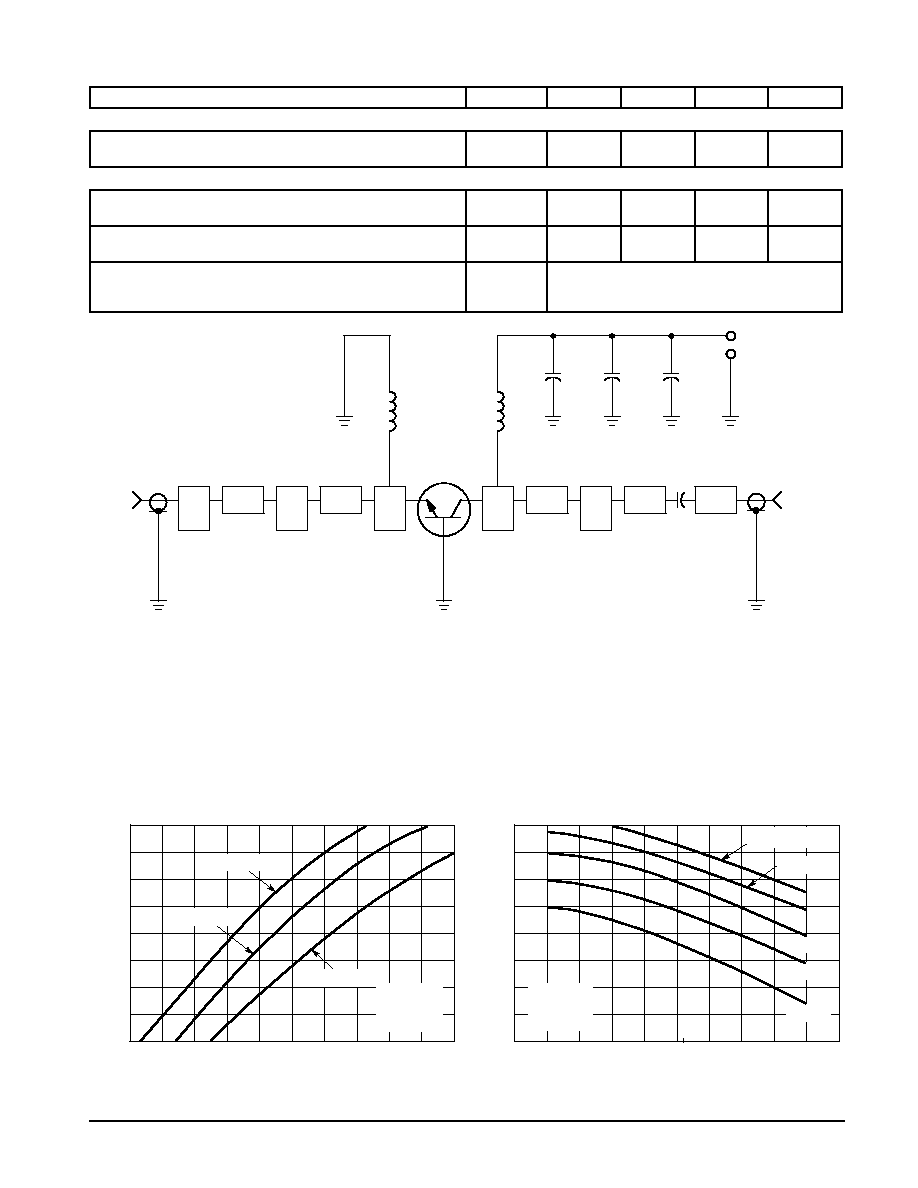
Figure 2. Output Power versus Input Power
Figure 3. Output Power versus Frequency
200
150
100
50
0
5
10
15
20
25
0
Pin, INPUT POWER (WATTS pk)
P
, OUTPUT
POWER
(W
A
TTS pk)
out
f, FREQUENCY (MHz)
P
, OUTPUT
POWER
(W
A
TTS pk)
out
VCC = 50 V
tp = 10
µ
s
D = 1%
Pin = 20 W pk
VCC = 50 V
tp = 10
µ
s
D = 1%
f = 960 MHz
1090 MHz
1215 MHz
200
150
100
50
0
960
1090
1215
17.5 W pk
12.5 W pk
10 W pk
15 W pk

3
MRF1150MA MRF1150MB
MOTOROLA RF DEVICE DATA
Figure 4. Output Power versus Supply Voltage
Figure 5. Power Gain versus Frequency
Figure 6. Series Equivalent Input/Output Impedance
f
MHz
Zin
Ohms
ZOL*
Ohms
960
1090
1215
1.5 + j9.6
5.0 + j7.5
2.4 + j5.6
2.6 + j4.1
2.7 + j4.6
2.8 + j5.3
Pout = 150 W pk VCC = 50 V
tp = 10
µ
s
D = 1%
G
PB
, POWER GAIN (dB)
f = 1090 MHz
tp = 10
µ
s
D = 1%
Po = 150 W pk
VCC = 50 V
tp = 10
µ
s
D = 1%
20
10
20
30
40
50
0
VCC, SUPPLY VOLTAGE (VOLTS)
P
, OUTPUT
POWER
(W
A
TTS pk)
out
14
12
10
8
6
4
960
1090
1215
f, FREQUENCY (MHz)
5
15
25
35
45
Pin = 20 W pk
17.5 W pk
12.5 W pk
15 W pk
10 W pk
200
150
100
50
ZOL* = Conjugate of the optimum load
ZOL* =
impedance into which the device
ZOL* =
output operates at a given output
ZOL* =
power, voltage, and frequency.
Zin
f = 960 MHz
1215
ZOL*
1090
0
5.0
10
f = 960 MHz
1215
1090
15
5.0
10
15
Figure 7. Typical Pulse Performance
Pout = 150 W pk
VCC = 50 V
tp = 10
µ
s
D = 1%
SCALE
2
µ
s/DIV
MRF1150MA MRF1150MB
4
MOTOROLA RF DEVICE DATA
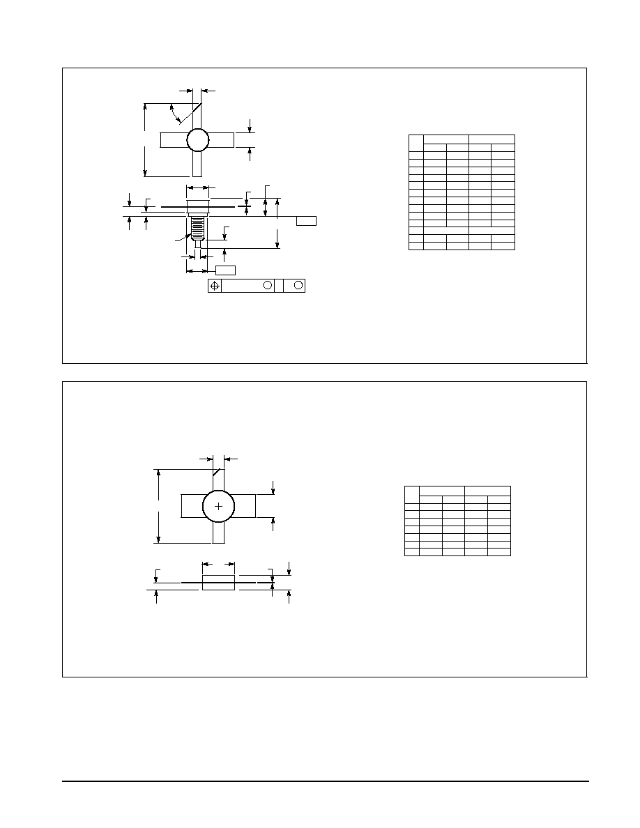
PACKAGE DIMENSIONS
CASE 332≠04
ISSUE D
(MRF1150MA)
NOTES:
1. DIMENSION K APPLIES TWO PLACES.
2. DIMENSIONING AND TOLERANCING PER ANSI
Y14.5M, 1973.
STYLE 1:
PIN 1. BASE
2. EMITTER
3. BASE
4. COLLECTOR
SEATING
PLANE
≠T≠
K
M
L
D
A
4
1
3
2
8≠32 UNC 2A
F
H
E
U
C
N
≠B≠
J
M
0.76 (0.030)
B
M
T
DIM
MIN
MAX
MIN
MAX
INCHES
MILLIMETERS
A
6.86
7.62
0.270
0.300
B
6.10
6.60
0.240
0.260
C
16.26
16.76
0.640
0.660
D
4.95
5.21
0.195
0.205
E
1.40
1.65
0.055
0.065
F
2.67
4.32
0.105
0.170
H
1.40
1.65
0.055
0.065
J
0.08
0.18
0.003
0.007
K
15.24
≠≠≠
0.600
≠≠≠
L
2.41
2.67
0.095
0.105
M
45 NOM
45 NOM
N
4.97
6.22
0.180
0.245
U
2.92
3.68
0.115
0.145
_
_
CASE 332A≠03
ISSUE D
(MRF1150MB)
NOTES:
1. DIMENSIONING AND TOLERANCING PER ANSI
Y14.5M, 1982.
2. CONTROLLING DIMENSION: INCH.
STYLE 1:
PIN 1. BASE
2. EMITTER
3. BASE
4. COLLECTOR
K
F
D
SEATING
1
4
3
2
PLANE
H
A
J
C
DIM
MIN
MAX
MIN
MAX
MILLIMETERS
INCHES
A
0.270
0.290
6.86
7.36
C
0.115
0.135
2.93
3.42
D
0.195
0.205
4.96
5.20
F
0.095
0.105
2.42
2.66
H
0.050
0.070
1.27
1.77
J
0.003
0.007
0.08
0.17
K
0.600
≠≠≠
15.24
≠≠≠

5
MRF1150MA MRF1150MB
MOTOROLA RF DEVICE DATA
Motorola reserves the right to make changes without further notice to any products herein. Motorola makes no warranty, representation or guarantee regarding
the suitability of its products for any particular purpose, nor does Motorola assume any liability arising out of the application or use of any product or circuit, and
specifically disclaims any and all liability, including without limitation consequential or incidental damages. "Typical" parameters which may be provided in Motorola
data sheets and/or specifications can and do vary in different applications and actual performance may vary over time. All operating parameters, including "Typicals"
must be validated for each customer application by customer's technical experts. Motorola does not convey any license under its patent rights nor the rights of
others. Motorola products are not designed, intended, or authorized for use as components in systems intended for surgical implant into the body, or other
applications intended to support or sustain life, or for any other application in which the failure of the Motorola product could create a situation where personal injury
or death may occur. Should Buyer purchase or use Motorola products for any such unintended or unauthorized application, Buyer shall indemnify and hold Motorola
and its officers, employees, subsidiaries, affiliates, and distributors harmless against all claims, costs, damages, and expenses, and reasonable attorney fees
arising out of, directly or indirectly, any claim of personal injury or death associated with such unintended or unauthorized use, even if such claim alleges that
Motorola was negligent regarding the design or manufacture of the part. Motorola and are registered trademarks of Motorola, Inc. Motorola, Inc. is an Equal
Opportunity/Affirmative Action Employer.
Mfax is a trademark of Motorola, Inc.
How to reach us:
USA / EUROPE / Locations Not Listed: Motorola Literature Distribution;
JAPAN: Nippon Motorola Ltd.: SPD, Strategic Planning Office, 4≠32≠1,
P.O. Box 5405, Denver, Colorado 80217. 303≠675≠2140 or 1≠800≠441≠2447
Nishi≠Gotanda, Shinagawa≠ku, Tokyo 141, Japan. 81≠3≠5487≠8488
Mfax
TM
: RMFAX0@email.sps.mot.com ≠ TOUCHTONE 602≠244≠6609
ASIA/PACIFIC: Motorola Semiconductors H.K. Ltd.; 8B Tai Ping Industrial Park,
≠ US & Canada ONLY 1≠800≠774≠1848
51 Ting Kok Road, Tai Po, N.T., Hong Kong. 852≠26629298
INTERNET: http://motorola.com/sps
MRF1150MA/D