1
MRF18030BR3 MRF18030BSR3
MOTOROLA RF DEVICE DATA
The RF MOSFET Line
RF Power Field Effect Transistors
N≠Channel Enhancement≠Mode Lateral MOSFETs
Designed for GSM and EDGE base station applications with frequencies
from 1.8 to 2.0 GHz. Suitable for FM, TDMA, CDMA and multicarrier amplifier
applications. Specified for GSM 1930 ≠ 1990 MHz.
∑ Typical GSM Performance:
Power Gain ≠ 14 dB (Typ) @ 30 Watts
Efficiency ≠ 50% (Typ) @ 30 Watts
∑ Internally Matched, Controlled Q, for Ease of Use
∑ High Gain, High Efficiency and High Linearity
∑ Integrated ESD Protection
∑ Designed for Maximum Gain and Insertion Phase Flatness
∑ Capable of Handling 5:1 VSWR, @ 26 Vdc, 30 W CW Output Power
∑ Excellent Thermal Stability
∑ Available in Tape and Reel. R3 Suffix = 250 Units per 32 mm,
13 inch Reel.
MAXIMUM RATINGS
Rating
Symbol
Value
Unit
Drain≠Source Voltage
V
DSS
65
Vdc
Gate≠Source Voltage
V
GS
+15, ≠0.5
Vdc
Total Device Dissipation @ T
C
= 25
∞C
Derate above 25
∞C
P
D
83.3
0.48
Watts
W/
∞C
Storage Temperature Range
T
stg
≠65 to +200
∞C
Operating Junction Temperature
T
J
200
∞C
ESD PROTECTION CHARACTERISTICS
Test Conditions
Class
Human Body Model
2 (Minimum)
Machine Model
M3 (Minimum)
THERMAL CHARACTERISTICS
Characteristic
Symbol
Max
Unit
Thermal Resistance, Junction to Case
R
JC
2.1
∞C/W
NOTE ≠ CAUTION ≠ MOS devices are susceptible to damage from electrostatic charge. Reasonable precautions in handling and
packaging MOS devices should be observed.
Order this document
by MRF18030B/D
MOTOROLA
SEMICONDUCTOR TECHNICAL DATA
MRF18030BR3
MRF18030BSR3
GSM/GSM EDGE 1.93 ≠ 1.99 GHz,
30 W, 26 V
LATERAL N≠CHANNEL
RF POWER MOSFETs
CASE 465E≠03, STYLE 1
NI≠400
MRF18030BR3
CASE 465F≠03, STYLE 1
NI≠400S
MRF18030BSR3
Motorola, Inc. 2002
REV 2

MRF18030BR3 MRF18030BSR3
2
MOTOROLA RF DEVICE DATA
ELECTRICAL CHARACTERISTICS
(T
C
= 25
∞C, 50 ohm system unless otherwise noted)
Characteristic
Symbol
Min
Typ
Max
Unit
OFF CHARACTERISTICS
Drain≠Source Breakdown Voltage
(V
GS
= 0 Vdc, I
D
= 20
µAdc)
V
(BR)DSS
65
--
--
Vdc
Zero Gate Voltage Drain Current
(V
DS
= 26 Vdc, V
GS
= 0 Vdc)
I
DSS
--
--
1
µAdc
Gate≠Source Leakage Current
(V
GS
= 5 Vdc, V
DS
= 0 Vdc)
I
GSS
--
--
1
µAdc
ON CHARACTERISTICS
Gate Threshold Voltage
(V
DS
= 10 Vdc, I
D
= 100
µAdc)
V
GS(th)
2
3
4
Vdc
Gate Quiescent Voltage
(V
DS
= 26 Vdc, I
D
= 250 mAdc)
V
GS(Q)
2
3.9
4.5
Vdc
Drain≠Source On≠Voltage
(V
GS
= 10 Vdc, I
D
= 1 Adc)
V
DS(on)
--
0.29
0.4
Vdc
Forward Transconductance
(V
DS
= 10 Vdc, I
D
= 1 Adc)
g
fs
--
2
--
S
DYNAMIC CHARACTERISTICS
Reverse Transfer Capacitance (1)
(V
DS
= 26 Vdc
± 30 mV(rms)ac @ 1 MHz, V
GS
= 0 Vdc)
C
rss
--
1.3
--
pF
FUNCTIONAL TESTS (In Motorola Test Fixture) (2)
Output Power, 1 dB Compression Point
(V
DD
= 26 Vdc, I
DQ
= 250 mA, f = 1930 ≠ 1990 MHz)
P1dB
27
30
--
Watts
Common≠Source Amplifier Power Gain @ 30 W
(V
DD
= 26 Vdc, I
DQ
= 250 mA, f = 1930 ≠ 1990 MHz)
G
ps
13
14
--
dB
Drain Efficiency @ 30 W
(V
DD
= 26 Vdc, I
DQ
= 250 mA, f = 1930 ≠ 1990 MHz)
46.5
50
--
%
Input Return Loss @ 30 W
(V
DD
= 26 Vdc, I
DQ
= 250 mA, f = 1930 ≠ 1990 MHz)
IRL
--
≠12
≠9
dB
Output Mismatch Stress @ 30 W
(V
DD
= 26 Vdc, I
DQ
= 250 mA, f1 = 1930 ≠ 1990 MHz,
VSWR = 5:1, All Phase Angles at Frequency of Tests)
No Degradation In Output Power
Before and After Test
(1) Part is internally matched both on input and output.
(2) Device specifications obtained on a Production Test Fixture.
3
MRF18030BR3 MRF18030BSR3
MOTOROLA RF DEVICE DATA
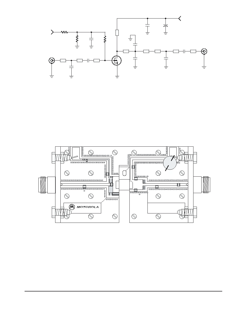
C1
1.8 pF, 100B Chip Capacitor
C2
0.8 pF, 100B Chip Capacitor
C3
0.8 pF, 100B Chip Capacitor
C4, C5
1.2 pF, 100B Chip Capacitors
C6, C7, C8
8.2 pF, 100B Chip Capacitors
C9
220
mF, 63 V Electrolytic Capacitor
R1
1.0 k
, 1/8 W Chip Resistor (0805)
R2, R3
10 k
, 1/8 W Chip Resistors (0805)
Z1
0.496
x 0.087 Microstrip
Z2
1.022
x 0.087 Microstrip
Z3
0.257
x 0.633 Microstrip
Z4
0.189
x 0.394 Microstrip
Z5
0.335
x 0.394 Microstrip
Z6
0.616
x 0.087 Microstrip
Z7
0.845
x 0.087 Microstrip
Z8
0.366
x 0.087 Microstrip
Z9
0.500 x 0.087 Microstrip
Figure 1. 1930 ≠ 1990 MHz Test Fixture Schematic
Figure 2. 1930 ≠ 1990 MHz Test Fixture Component Layout
RF
INPUT
RF
OUTPUT
Z1
V
GG
C2
C6
Z3
DUT
V
DD
Z4
Z5
C1
Z7
R2
C7
R1
C9
C8
+
Z2
R3
Z9
Z8
C3
C5
C4
Z6
VBIAS
Ground
Ground
VSUPPLY
R2
MRF18030B
(bias)
(supply)
R3
C7
R1
C2
C1
C8
C4
C5
C3
C6
C9
CUT
OUT
AREA
MRF18030BR3 MRF18030BSR3
4
MOTOROLA RF DEVICE DATA
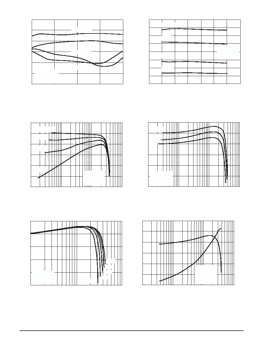
Figure 3. Wideband Gain and IRL at 30 W and
15 W Output Power
Figure 4. Output Power versus Frequency
Figure 5. Power Gain versus Output Power
Figure 6. Power Gain versus Output Power
Figure 7. Power Gain versus Output Power
Figure 8. Power Gain and Efficiency versus
Output Power
INPUT
RETURN LOSS (dB)
IRL,
10
1850
-30
IRL @ 30 W
G
ps
@ 15 W
V
DD
= 26 Vdc
I
DQ
= 250 mA
T = 25_C
f, FREQUENCY (MHz)
G
ps
, POWER GAIN (dB)
G
ps
@ 30 W
IRL @ 15 W
11
-25
12
-20
13
-15
14
-10
15
-5
16
0
1900
1950
2000
2050
f, FREQUENCY (MHz)
2020
0
40
1880
P
in
= 2 W
V
DD
= 26 Vdc
I
DQ
= 250 mA
T = 25_C
1 W
0.5 W
0.25 W
5
10
15
20
25
30
35
1900
1920
1940
1960
1980
2000
P out
, OUTPUT
POWER (W
A
TTS)
100
16
0.1
P
out
, OUTPUT POWER (WATTS)
G
ps
, POWER GAIN (dB)
I
DQ
= 400 mA
300 mA
V
DD
= 26 Vdc
f = 1960 MHz
T = 25_C
200 mA
100 mA
15
14
13
12
11
10
1
10
85_C
100
15
0.1
T = 25_C
V
DD
= 26 Vdc
I
DQ
= 250 mA
f = 1960 MHz
P
out
, OUTPUT POWER (WATTS)
G
ps
, POWER GAIN (dB)
55_C
14
13
12
11
10
9
1
10
0
100
16
0.1
G
ps
h
V
DD
= 26 Vdc
I
DQ
= 250 mA
f = 1960 MHz
T = 25_C
P
out
, OUTPUT POWER (WATTS)
G
ps
, POWER GAIN (dB)
15
14
13
12
11
10
50
40
30
20
10
60
1
10
,
DRAIN EFFICIENCY
(
%
)
100
15
V
DD
= 22 V
24 V
I
DQ
= 250 mA
f = 1960 MHz
T = 25_C
P
out
, OUTPUT POWER (WATTS)
G
ps
, POWER GAIN (dB)
28 V
30 V
30 V
14
13
12
11
10
1
10
26 V

5
MRF18030BR3 MRF18030BSR3
MOTOROLA RF DEVICE DATA
Figure 9. Series Equivalent Input and Output Impedance
f
MHz
Z
in
Z
OL
*
1710
1785
1805
2.92 + j8.24
4.15 + j10.38
3.84 + j9.75
4.18 + j9.06
4.59 + j9.46
4.98 + j9.06
Z
in
= Complex conjugate of the source impedance.
Z
OL
* = Complex conjugate of the optimum load
impedance at a given power, voltage,
bias current and frequency.
Note: Z
OL
* was chosen based on tradeoffs between gain,
output power, and drain efficiency.
V
DD
= 26 V, I
DQ
= 250 mA, P
out
= 30 W (CW)
Zin
Z OL*
Input
Matching
Network
Device
Under Test
Output
Matching
Network
Z
in
f = 2110 MHz
f = 1710 MHz
1840
1880
1960
4.04 + j10.22
6.20 + j12.29
6.12 + j12.29
6.10 + j7.63
5.83 + j6.89
5.55 + j6.33
1990
2110
15.19 + j11.85
8.61 + j12.10
5.93 + j6.66
3.82 + j5.33
f = 1710 MHz
Z
OL
*
f = 2110 MHz
Z
o
= 25