 | –≠–ª–µ–∫—Ç—Ä–æ–Ω–Ω—ã–π –∫–æ–º–ø–æ–Ω–µ–Ω—Ç: MRF18085B | –°–∫–∞—á–∞—Ç—å:  PDF PDF  ZIP ZIP |

1
MRF18085BR3 MRF18085BLSR3
MOTOROLA RF DEVICE DATA
The RF MOSFET Line
RF Power Field Effect Transistors
N-Channel Enhancement-Mode Lateral MOSFETs
Designed for GSM and GSM EDGE base station applications with
frequencies from 1.9 to 2.0 GHz. Suitable for TDMA, CDMA, and multicarrier
amplifier applications.
∑ GSM and GSM EDGE Performance, Full Frequency Band (1930 - 1990
MHz)
Power Gain - 12.5 dB (Typ) @ 85 Watts CW
Efficiency - 50% (Typ) @ 85 Watts CW
∑ Internally Matched, Controlled Q, for Ease of Use
∑ High Gain, High Efficiency, and High Linearity
∑ Integrated ESD Protection
∑ Designed for Maximum Gain and Insertion Phase Flatness
∑ Capable of Handling 5:1 VSWR, @ 26 Vdc, @ P1dB Output Power,
@ f = 1930 MHz
∑ Excellent Thermal Stability
∑ Characterized with Series Equivalent Large-Signal Impedance Parameters
∑ Available with Low Gold Plating Thickness on Leads. L Suffix Indicates
40µ Nominal.
∑ In Tape and Reel. R3 Suffix = 250 Units per 56 mm, 13 inch Reel.
MAXIMUM RATINGS
Rating
Symbol
Value
Unit
Drain-Source Voltage
V
DSS
65
Vdc
Gate-Source Voltage
V
GS
-0.5, +15
Vdc
Total Device Dissipation @ T
C
= 25∞C
Derate above 25∞C
P
D
273
1.56
Watts
W/∞C
Storage Temperature Range
T
stg
- 65 to +150
∞C
Operating Junction Temperature
T
J
200
∞C
THERMAL CHARACTERISTICS
Characteristic
Symbol
Value (1)
Unit
Thermal Resistance, Junction to Case
R
JC
0.79
∞C/W
ESD PROTECTION CHARACTERISTICS
Test Conditions
Class
Human Body Model
1 (Minimum)
Machine Model
M3 (Minimum)
(1) Refer to AN1955/D, Thermal Measurement Methodology of RF Power Amplifiers. Go to http://www.motorola.com/semiconductors/rf.
Select Documentation/Application Notes - AN1955.
NOTE - CAUTION - MOS devices are susceptible to damage from electrostatic charge. Reasonable precautions in handling and
packaging MOS devices should be observed.
Order this document
by MRF18085B/D
MOTOROLA
SEMICONDUCTOR TECHNICAL DATA
MRF18085BR3
MRF18085BLSR3
GSM/GSM EDGE
1.9 - 1.99 GHz, 85 W, 26 V
LATERAL N-CHANNEL
RF POWER MOSFETs
CASE 465-06, STYLE 1
NI-780
MRF18085BR3
CASE 465A-06, STYLE 1
NI-780S
MRF18085BLSR3
Motorola, Inc. 2004
REV 3
F
r
e
e
s
c
a
l
e
S
e
m
i
c
o
n
d
u
c
t
o
r
,
I
Freescale Semiconductor, Inc.
For More Information On This Product,
Go to: www.freescale.com
n
c
.
.
.

MRF18085BR3 MRF18085BLSR3
2
MOTOROLA RF DEVICE DATA
ELECTRICAL CHARACTERISTICS
(T
C
= 25∞C unless otherwise noted)
Characteristic
Symbol
Min
Typ
Max
Unit
OFF CHARACTERISTICS
Drain-Source Breakdown Voltage
(V
GS
= 0 Vdc, I
D
= 100 µAdc)
V
(BR)DSS
65
--
--
Vdc
Zero Gate Voltage Drain Current
(V
DS
= 26 Vdc, V
GS
= 0 Vdc)
I
DSS
--
--
10
µAdc
Gate-Source Leakage Current
(V
GS
= 5 Vdc, V
DS
= 0 Vdc)
I
GSS
--
--
1
µAdc
ON CHARACTERISTICS
Gate Threshold Voltage
(V
DS
= 10 Vdc, I
D
= 200 µAdc)
V
GS(th)
2
--
4
Vdc
Gate Quiescent Voltage
(V
DS
= 26 Vdc, I
D
= 600 mAdc)
V
GS(Q)
2.5
3.9
4.5
Vdc
Drain-Source On-Voltage
(V
GS
= 10 Vdc, I
D
= 2 Adc)
V
DS(on)
--
0.18
0.21
Vdc
Forward Transconductance
(V
DS
= 10 Vdc, I
D
= 2 Adc)
g
fs
--
6.0
--
S
DYNAMIC CHARACTERISTICS
Reverse Transfer Capacitance (1)
(V
DS
= 26 Vdc, V
GS
= 0, f = 1 MHz)
C
rss
--
3.6
--
pF
FUNCTIONAL TESTS (In Motorola Test Fixture, 50 ohm system)
Common-Source Amplifier Power Gain @ 85 W
(V
DD
= 26 Vdc, I
DQ
= 800 mA, f = 1930 - 1990 MHz)
G
ps
11.5
12.5
--
dB
Drain Efficiency @ 85 W
(V
DD
= 26 Vdc, I
DQ
= 800 mA, f = 1930 - 1990 MHz)
46
50
--
%
Input Return Loss @ 85 W
(V
DD
= 26 Vdc, I
DQ
= 800 mA, f = 1930 - 1990 MHz)
IRL
--
-12
-9
dB
P1 dB Output Power
(V
DD
= 26 Vdc, I
DQ
= 800 mA, f = 1930 - 1990 MHz)
P1dB
80
90
--
Watts
Output Mismatch Stress @ P1dB
(V
DD
= 26 Vdc, I
DQ
= 600 mA, f = 1930 MHz,
VSWR = 5:1, All Phase Angles at Frequency of Tests)
No Degradation In Output Power
Before and After Test
(1) Part is internally matched both on input and output.
F
r
e
e
s
c
a
l
e
S
e
m
i
c
o
n
d
u
c
t
o
r
,
I
Freescale Semiconductor, Inc.
For More Information On This Product,
Go to: www.freescale.com
n
c
.
.
.

3
MRF18085BR3 MRF18085BLSR3
MOTOROLA RF DEVICE DATA
V
BIAS
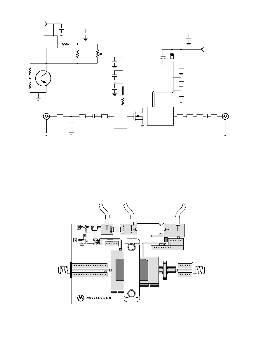
C1, C10
1.0 nF Chip Capacitors, B Case, ATC
C2
10 mF, 35 V Tantalum Capacitor
C3, C6
10 pF Chip Capacitors, B Case, ATC
C4
3.3 pF Chip Capacitor, B Case, ATC
C5
4.7 pF Chip Capacitor, B Case, ATC
C7, C8
100 nF Chip Capacitors, ACCU-P (1206)
C9
3.9 pF Chip Capacitor, B Case, ATC
C11
470 mF, 63 V Electrolytic Capacitor
R1, R2
1.0 kW Chip Resistors (0805)
R3
2 x 18 kW Chip Resistor (1206)
Z1
1.654 x 0.082 Microstrip
Z2
0.207 x 0.082 Microstrip
Z3
0.362 x 1.260 Microstrip
Z4
0.583 x 0.669 Microstrip
Z5
0.449 x 0.179 Microstrip
Z6
0.877 x 0.082 Microstrip
Z7
0.326 x 0.082 Microstrip
PCB
0.030 Glass Teflon
(e
r
= 2.55)
Figure 1. 1.93 - 1.99 GHz Test Fixture Schematic
Figure 2. 1.93 - 1.99 GHz Test Fixture Component Layout
Ground
Ground
A1
A2
C11
MRF18085B
VBIAS
VSUPPLY
C2
R1
R2
C1
R3
C8
C9
C4
C5
C3
C7
C10
C6
RF
INPUT
RF
OUTPUT
Z1
C5
C6
C8
Z3
DUT
Z5
Z6
Z7
C1
R3
C11
C10
+
Z2
R1
C2
C7
V
SUPPLY
R2
+
C4
C9
Z4
C3
Rev 0
F
r
e
e
s
c
a
l
e
S
e
m
i
c
o
n
d
u
c
t
o
r
,
I
Freescale Semiconductor, Inc.
For More Information On This Product,
Go to: www.freescale.com
n
c
.
.
.
MRF18085BR3 MRF18085BLSR3
4
MOTOROLA RF DEVICE DATA
C10
V
SUPPLY
C2
C1
R1
R2
R5
R3
R4
Z5
ŒŒŒ
ŒŒŒ
ŒŒŒ
T1
T2
C5
Z4
RF
INPUT
RF
OUTPUT
Z2
C7
Z9
+
Figure 3. 1.93 - 1.99 GHz GSM EDGE Optimized Demo Board Schematic
Figure 4. 1.93 - 1.99 GHz GSM EDGE Optimized Demo Board Component Layout
B1
Short RF Ferrite Bead, #27 430119447
C1, C2
1 mF Chip Capacitors, ACCU-P (0805)
C3, C4
1 nF Chip Capacitors, ACCU-P (0805)
C5
10 pF Chip Capacitor, ACCU-P (0805)
C7
1.5 pF Chip Capacitor, ACCU-P (0805)
C8
8.2 pF Chip Capacitor, ACCU-P (0805)
C9
1.0 pF Chip Capacitor, ACCU-P (0805)
C10
100 mF, 63 V Electrolytic Capacitor
C11, C12
10 nF Chip Capacitors (0805)
C13
10 mF, 35 V Tantalum Capacitor
C14
8.2 pF Chip Capacitor, ACCU-P (0805)
R1
10 Chip Resistor (0805)
R2
1 k Chip Resistor (0805)
R3
1.2 k Chip Resistor (0805)
R4
2.2 k Chip Resistor (0805)
R5
5 k Chip Resistor (0805)
R6, R7
9 Chip Resistors (1206) (18 x 18 )
T1
Voltage Regulator, Micro-8, Motorola #LP2951
T2
NPN Bipolar Transistor, SOT-23, Motorola #BC847
Z1 - Z9
Printed Transmission Lines
Substrate
0.5 mm Rogers 4350 (e
r
= 3.53)
C3
C4
Z3
Z1
C9
C11
C8
Z8
Z7
Z6
C13
V
BIAS
C14
R6
D
C11
C4
C5
C8
C7
C9
C13
C14
C3
C2
R5
T2
R4
R3
R2
C1
R1
T1
R6
C10
+
V
Ground
SUPPLY
MRF18085
VBIAS
B1
+
C12
R7
B1
C12
F
r
e
e
s
c
a
l
e
S
e
m
i
c
o
n
d
u
c
t
o
r
,
I
Freescale Semiconductor, Inc.
For More Information On This Product,
Go to: www.freescale.com
n
c
.
.
.
5
MRF18085BR3 MRF18085BLSR3
MOTOROLA RF DEVICE DATA
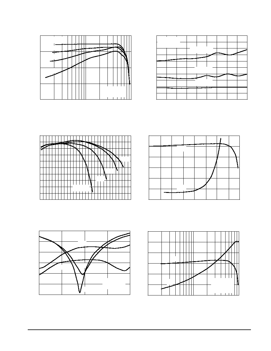
TYPICAL CHARACTERISTICS
(Performed on a GSM EDGE Optimized Demo Board)
Figure 5. Power Gain versus Output Power
P
out
, OUTPUT POWER (WATTS)
10
Figure 6. Error Vector Magnitude versus
Frequency
0
f, FREQUENCY (GHz)
5
1.5
G
ps
, POWER GAIN (dB)
1.91
EVM, ERROR VECT
OR
MAGNITUDE
(%)
Figure 7. Power Gain versus Output Power
14
P
out
, OUTPUT POWER (WATTS)
9
Figure 8. EVM and Gain versus Output Power
P
out
, OUTPUT POWER (dBm) AVG.
1
0
34
36
6
10
0.5
100
2.5
1.98
1.95
11
, DRAIN EFFICIENCY
(%)
0
20
Figure 9. Power Gain and IRL
versus Frequency
14
f, FREQUENCY (GHz)
11
1.85
13.5
2.05
1.95
1.90
2.00
10
13
14
1.97
40
38
50
14
13
11
9
8
11
12
1.94
1.96
3.5
60
80
12
13
3
2
4
5
10
G
ps
, POWER GAIN (dB)
-30
-15
-25
-20
-5
-10
12
11.5
1
1.93
1.99
1.92
4.5
100
2
1
3
4
2.0
Figure 10. Power Gain and Efficiency
versus Output Power
16
P
out
, OUTPUT POWER (WATTS)
10
14
10
1
100
G
ps
, POWER GAIN (dB)
60
30
10
0
20
50
40
12
EVM, ERROR VECT
OR
MAGNITUDE
(%)
G
ps
, POWER GAIN (dB)
42
44
46
48
15
13
11
12.5
13
V
DD
= 26 Vdc
f = 1.96 GHz
600 mA
400 mA
800 mA
I
DQ
= 1000 mA
P
out
= 38 W Avg.
28 W Avg.
19 W Avg.
V
DD
= 26 Vdc
I
DQ
= 800 mA
24 V
V
DD
= 20 V
32 V
28 V
G
ps
EVM
V
DD
= 26 Vdc
I
DQ
= 800 mA
30 W
30 W
80 W
80 W
h
G
ps
9.5
10.5
11.5
12.5
13.5
G
ps
, POWER GAIN (dB)
40
12
-35
V
DD
= 26 Vdc
I
DQ
= 800 mA
f = 1.96 GHz
F
r
e
e
s
c
a
l
e
S
e
m
i
c
o
n
d
u
c
t
o
r
,
I
Freescale Semiconductor, Inc.
For More Information On This Product,
Go to: www.freescale.com
n
c
.
.
.