
1
MRF19045R3 MRF19045SR3
MOTOROLA RF DEVICE DATA
The RF MOSFET Line
RF Power Field Effect Transistors
N≠Channel Enhancement≠Mode Lateral MOSFETs
Designed for PCN and PCS base station applications with frequencies from
1 . 9 t o 2 . 0 G H z . S u i t a b l e f o r T D M A , C D M A a n d m u l t i c a r r i e r a m p l i f i e r
applications.
∑ Typical CDMA Performance @ 1960 MHz, 26 Volts, I
DQ
= 550 mA
Multi≠carrier CDMA Pilot, Sync, Paging, Traffic Codes 8 Through 13
Output Power -- 9.5 Watts Avg.
Power Gain -- 14.9 dB
Efficiency -- 23.5%
Adjacent Channel Power --
885 kHz: ≠50 dBc @ 30 kHz BW
IM3 -- ≠37 dBc
∑ 100% Tested Under 2≠Carrier N≠CDMA
∑ Internally Matched, Controlled Q, for Ease of Use
∑ High Gain, High Efficiency and High Linearity
∑ Integrated ESD Protection
∑ Designed for Maximum Gain and Insertion Phase Flatness
∑ Capable of Handling 5:1 VSWR, @ 26 Vdc, 1.93 GHz, 45 Watts CW
Output Power
∑ Excellent Thermal Stability
∑ Characterized with Series Equivalent Large≠Signal Impedance Parameters
∑ In Tape and Reel. R3 Suffix = 250 Units per 32 mm, 13 Inch Reel.
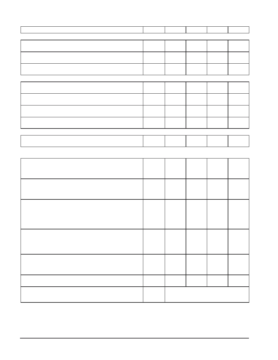
MAXIMUM RATINGS
Rating
Symbol
Value
Unit
Drain≠Source Voltage
V
DSS
65
Vdc
Gate≠Source Voltage
V
GS
≠0.5, +15
Vdc
Total Device Dissipation @ T
C
= 25
∞C
Derate above 25
∞C
P
D
105
0.60
Watts
W/
∞C
Storage Temperature Range
T
stg
≠65 to +200
∞C
Operating Junction Temperature
T
J
200
∞C
ESD PROTECTION CHARACTERISTICS
Test Conditions
Class
Human Body Model
2 (Minimum)
Machine Model
M3 (Minimum)
THERMAL CHARACTERISTICS
Characteristic
Symbol
Max
Unit
Thermal Resistance, Junction to Case
R
JC
1.65
∞C/W
NOTE ≠ CAUTION ≠ MOS devices are susceptible to damage from electrostatic charge. Reasonable precautions in handling and
packaging MOS devices should be observed.
Order this document
by MRF19045/D
MOTOROLA
SEMICONDUCTOR TECHNICAL DATA
MRF19045R3
MRF19045SR3
1990 MHz, 45 W, 26 V
LATERAL N≠CHANNEL
RF POWER MOSFETs
CASE 465E≠03, STYLE 1
NI≠400
MRF19045R3
CASE 465F≠03, STYLE 1
NI≠400S
MRF19045SR3
Motorola, Inc. 2002
REV 3
MRF19045R3 MRF19045SR3
2
MOTOROLA RF DEVICE DATA
ELECTRICAL CHARACTERISTICS
(T
C
= 25
∞C unless otherwise noted)
Characteristic
Symbol
Min
Typ
Max
Unit
OFF CHARACTERISTICS
Drain≠Source Breakdown Voltage
(V
GS
= 0 Vdc, I
D
= 100
µAdc)
V
(BR)DSS
65
--
--
Vdc
Zero Gate Voltage Drain Current
(V
DS
= 26 Vdc, V
GS
= 0 Vdc)
I
DSS
--
--
10
µAdc
Gate≠Source Leakage Current
(V
GS
= 5 Vdc, V
DS
= 0 Vdc)
I
GSS
--
--
1
µAdc
ON CHARACTERISTICS (DC)
Gate Threshold Voltage
(V
DS
= 10 Vdc, I
D
= 100
µAdc)
V
GS(th)
2
--
4
Vdc
Gate Quiescent Voltage
(V
DS
= 26 Vdc, I
D
= 550 mAdc)
V
GS(Q)
3
3.8
5
Vdc
Drain≠Source On≠Voltage
(V
GS
= 10 Vdc, I
D
= 1 Adc)
V
DS(on)
--
0.19
0.21
Vdc
Forward Transconductance
(V
DS
= 10 Vdc, I
D
= 2 Adc)
g
fs
--
4.2
--
S
DYNAMIC CHARACTERISTICS
Reverse Transfer Capacitance (1)
(V
DS
= 26 Vdc, V
GS
= 0, f = 1.0 MHz)
C
rss
--
1.8
--
pF
FUNCTIONAL TESTS (In Motorola Test Fixture, 50 ohm system) 2≠carrier N≠CDMA, 1.2288 MHz Channel Bandwidth, IM3 measured in
1.2288 MHz Integrated Bandwidth. ACPR measured in 30 kHz Integrated Bandwidth.
Common≠Source Amplifier Power Gain
(V
DD
= 26 Vdc, P
out
= 9.5 W Avg, 2≠Carrier N≠CDMA,
I
DQ
= 550 mA, f1 = 1930 MHz, f2 = 1932.5 MHz and f1 =1987.5 MHz,
f2 = 1990 MHz)
G
ps
13
14.5
--
dB
Drain Efficiency
(V
DD
= 26 Vdc, P
out
= 9.5 W Avg, 2≠Carrier N≠CDMA,
I
DQ
= 550 mA, f1 = 1930 MHz, f2 = 1932.5 MHz and f1 =1987.5 MHz,
f2 = 1990 MHz)
21
23.5
--
%
3rd Order Intermodulation Distortion
(V
DD
= 26 Vdc, P
out
= 9.5 W Avg, 2≠Carrier N≠CDMA,
I
DQ
= 550 mA, f1 = 1930 MHz, f2 = 1932.5 MHz and f1 =1987.5 MHz,
f2 = 1990 MHz; IM3 Measured in a 1.2288 MHz Integrated Bandwidth
Centered at f1 ≠2.5 Mhz and f2 +2.5 MHz, Referenced to the Carrier
Channel Power)
IM3
--
≠37
≠35
dBc
Adjacent Channel Power Ratio
(V
DD
= 26 Vdc, P
out
= 9.5 W Avg, 2≠carrier N≠CDMA, I
DQ
= 550 mA,
f1 = 1930 MHz, f2 = 1932.5 MHz and f1 = 1987.5 MHz,
f2 = 1990 MHz; ACPR measured in a 30 kHz Integrated Bandwith
Centered at f1 ≠885 kHz and f2 +885 kHz)
ACPR
--
≠51
≠45
dBc
Input Return Loss
(V
DD
= 26 Vdc, P
out
= 9.5 W Avg, 2≠Carrier N≠CDMA,
I
DQ
= 550 mA, f1 = 1930 MHz, f2 = 1932.5 MHz and f1 =1987.5 MHz,
f2 = 1990 MHz)
IRL
--
≠16
≠9
dB
P
out
, 1 dB Compression Point
(V
DD
= 26 Vdc, I
DQ
= 550 mA, f = 1990 MHz)
P1dB
--
45
--
W
Output Mismatch Stress
(V
DD
= 26 Vdc, P
out
= 45 W CW, I
DQ
= 550 mA,
f = 1930 MHz, VSWR = 5:1, All Phase Angles at Frequency of Tests)
No Degradation In Output Power
Before and After Test
(1) Part is internally matched both on input and output.

3
MRF19045R3 MRF19045SR3
MOTOROLA RF DEVICE DATA
Figure 1. 1930 ≠ 1990 MHz 2-Carrier N-CDMA Test Circuit Schematic
RF
OUTPUT
Z3
Z4
C6
C1
R1
C3
+
C7
C5
C8
C2
Z6
Z7
V
DD
C12
C10
Z11
C9
Z8
C11
+
Z9
0.519
x 0.254 Microstrip
Z10
0.874
x 0.081 Microstrip
Z11
0.645
x 0.081 Microstrip
Board
3
x 5 Copper Clad PCB,
Arlon GX0300-55-22,
r
= 2.55
Printed Circuit
CMR Part Number 19045PC5.SKF
Board
Z1
1.336
x 0.081 Microstrip
Z2
0.693
x 0.081 Microstrip
Z3
1.033
x 0.047 Microstrip
Z4
0.468
x 0.047 Microstrip
Z5
0.271
x 0.460 Microstrip
Z6
0.263
x 0.930 Microstrip
Z7
1.165
x 0.047 Microstrip
Z8
0.216
x 0.047 Microstrip
NOTE: Z3, Z4, Z7, Z8 lengths and component placement tolerances are
±0.050.
Zx lengths are microstrip lengths between components, center-line to center-line.
All component and z-length tolerances are
±0.015, except as noted.
+
+
V
GG
RF
INPUT
Z1
Z2
Z5
W2
R4
+
Z9
Z10
C13
B2
R5
B2
W1
R3
B1
R2
C4
Table 1. 1930 ≠ 1990 MHz 2-Carrier N-CDMA Test Circuit Component Designations and Values
Designators
Description
B1, B2
0.120
x 0.333 x 0.100, Surface Mount Ferrite Beads, Fair Rite #2743019446
C1, C2
10
mF, 35 V Tantalum Surface Mount Chip Capacitors, Kemet #T495X106K035AS4394
C3, C11
0.1
mF Chip Capacitors, Kemet #CDR33BX104AKWS
C4, C8
24 pF Chip Capacitors, B Case, ATC #100B240JP500X
C5
470 pF Chip Capacitor, B Case, ATC #100B471JP200X
C6, C7
11 pF Chip Capacitors, B Case, ATC #100B110JP500X
C9, C10, C12
22
mF, 35 V Tantalum Surface Mount Chip Capacitors, Kemet #T491X226K035AS4394
C13
8.2 pF Chip Capacitor, B Case, ATC #100B8R2CP500X
R1
560 k
, 1/4 W Chip Resistor (0.08 x 0.13)
R2, R3, R4, R5
8.2
, 1/4 W Chip Resistors (0.08 x 0.13), Garrett Instruments #RM73B2B110JT
W1, W2
Solid Copper Buss Wire, 16 AWG
WS1, WS2
Beryllium Copper Wear Blocks (0.005
x 0.150 x 0.350) Nominal
Brass Banana Jack and Nut
Red Banana Jack and Nut
Green Banana Jack and Nut
Type "N" Jack Connectors, Omni-Spectra #3052-1648-10
4-40 Ph Head Screws, 0.125
long
4-40 Ph Head Screws, 0.312
long
4-40 Ph Head Screws, 0.625
long
4-40 Ph Rec. Hd. Screws, 0.625
long
MRF19045R3 MRF19045SR3
4
MOTOROLA RF DEVICE DATA
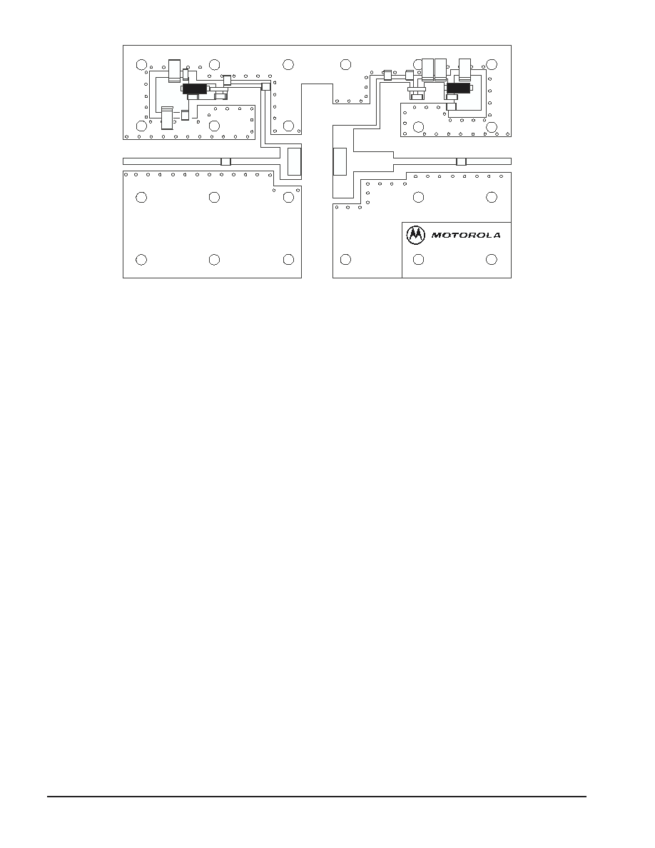
Figure 2. 1930 ≠ 1990 MHz 2-Carrier N-CDMA Test Circuit Component Layout
C1
C13
C12
W1
WS1
W2
B1
R1
R2
R3
R4
R5
B2
C2
C3
C4
C5
C6
C7 C8
C9 C10
MRF19045/S
Rev≠0
C11
WS2

5
MRF19045R3 MRF19045SR3
MOTOROLA RF DEVICE DATA
TYPICAL CHARACTERISTICS
5
10
15
20
25
30
35
1900
1930
1960
1990
2020
-60
-50
-40
-30
-20
-10
0
Figure 3. 2-Carrier N≠CDMA ACPR, IM3, Power Gain
and Drain Efficiency versus Output Power
Figure 4. 2-Carrier N-CDMA ACPR, IM3, Power Gain, IRL
and Drain Efficiency versus Output Power
Figure 5. 2-Carrier N-CDMA IM3
versus Output Power
P
out
, OUTPUT POWER (WATTS) (Avg. 2 Carrier N CDMA)
Figure 6. 2-Carrier N-CDMA ACPR
versus Output Power
13.5
ACPR,
ADJACENT
CHANNEL
POWER RA
TIO (dBc)
G
ps
, POWER GAIN (dB)
IM3,
THIRD ORDER
INTERMODULA
TION DIST
OR
TION (dBc)
, DRAIN EFFICIENCY
(%),
G
ps
, POWER GAIN (dB)
P
out
, OUTPUT POWER (WATTS) (Avg. 2 Carrier N CDMA)
IM3 (dBc),
ACPR (dBc)
0
5
10
15
20
25
30
35
40
1
2
3
4
5
6
7
8
9
10
11
12
-70
-65
-60
-55
-50
-45
-40
-35
-30
G
ps
ACPR
IM3
G
ps
ACPR
IM3
IRL
f, FREQUENCY (MHz)
IM3 (dBc),
ACPR (dBc),
IRL
(dB)
, DRAIN EFFICIENCY
(%),
G
ps
, POWER GAIN (dB)
-55
-50
-45
-40
-35
-30
0
1
9
10 11 12
350 mA
450 mA
700 mA
550 mA
V
DD
= 26 Vdc
I
DQ
= 550 mA
f1 = 1960 MHz, f2 = 1962.5 MHz
2
3
4
5
6
7
8
P
out
, OUTPUT POWER (WATTS) (Avg. 2 Carrier N CDMA)
0
1
9
10 11 12
2
3
4
5
6
7
8
-70
-55
-65
-60
-50
-45
Figure 7. 2-Carrier N-CDMA Power Gain
versus Output Power
P
out
, OUTPUT POWER (WATTS) (Avg. 2 Carrier N CDMA)
350 mA
450 mA
700 mA
550 mA
0
1
9
10 11 12
2
3
4
5
6
7
8
350 mA
450 mA
700 mA
550 mA
14.0
14.5
15.0
15.5
V
DD
= 26 Vdc
I
DQ
= 450 mA
f1 = 1960 MHz, f2 = 1960.1 MHz
1.2288 MHz Source Channel Bandwidth,
9 CH FWD Carrier
(9.8 dB Peak/Avg. Ratio @ 0.01%)
V
DD
= 26 Vdc, I
DQ
= 550 mA 2.5 MHz Carrier Spacing
9 CH FWD Carrier (9.8 dB Peak/Avg. Ratio @ 0.01%)
1.2288 MHz Source Channel Bandwidth
V
DD
= 26 Vdc
I
DQ
= 550 mA
f1 = 1960 MHz, f2 = 1962.5 MHz
1.2288 MHz Source Channel Bandwidth,
9 CH FWD Carrier
(9.8 dB Peak/Avg. Ratio @ 0.01%
Probability) (CCDF)
V
DD
= 26 Vdc, I
DQ
= 550 mA
f1 = 1960 MHz, f2 = 1962.5 MHz
1.2288 MHz Source Channel Bandwidth,
9 CH FWD Carrier
(9.8 dB Peak/Avg. Ratio @ 0.01% Probability) (CCDF)
Figure 8. CW Output Power, Power Gain and Drain
Efficiency versus Input Power
0
10
20
30
40
50
60
70
0.0
0.5
1.0
1.5
2.0
2.5
3.0
3.5
4.0
4.5
10
11
12
13
14
15
16
17
Gps
Pout
P1dB
P3dB
P
in
, INPUT POWER (WATTS CW)
, DRAIN EFFICIENCY
(%),
P
, OUTPUT
POWER (W
A
TTS CW)
out
G
ps
, POWER GAIN (dB)
V
DD
= 26 Vdc
I
DQ
= 550 mA
f = 1960 MHz