 | –≠–ª–µ–∫—Ç—Ä–æ–Ω–Ω—ã–π –∫–æ–º–ø–æ–Ω–µ–Ω—Ç: MRF21045 | –°–∫–∞—á–∞—Ç—å:  PDF PDF  ZIP ZIP |

1
MRF21045LR3 MRF21045LSR3
MOTOROLA RF DEVICE DATA
The RF MOSFET Line
RF Power Field Effect Transistors
N-Channel Enhancement-Mode Lateral MOSFETs
Designed for W-CDMA base station applications with frequencies from 2110
to 2170 MHz. Suitable for TDMA, CDMA and multicarrier amplifier applica-
tions. To be used in Class AB for PCN - PCS/cellular radio and WLL
applications.
∑ Typical 2-carrier W-CDMA Performance for V
DD
= 28 Volts, I
DQ
= 500 mA,
f1 = 2135 MHz, f2 = 2145 MHz, Channel Bandwidth = 3.84 MHz,
Adjacent Channels measured over 3.84 MHz Bandwidth at f1 -5 MHz
and f2 +5 MHz, Distortion Products measured over a 3.84 MHz Bandwidth
at f1 -10 MHz and f2 +10 MHz, Peak/Avg. = 8.3 dB @ 0.01% Probability
on CCDF.
Output Power -- 10 Watts Avg.
Efficiency -- 23.5%
Gain -- 15 dB
IM3 -- -37.5 dBc
ACPR -- -41 dBc
∑ Internally Matched, Controlled Q, for Ease of Use
∑ High Gain, High Efficiency and High Linearity
∑ Integrated ESD Protection
∑ Designed for Maximum Gain and Insertion Phase Flatness
∑ Capable of Handling 5:1 VSWR, @ 28 Vdc, 2170 MHz, 45 Watts CW
Output Power
∑ Excellent Thermal Stability
∑ Characterized with Series Equivalent Large-Signal Impedance Parameters
∑ Low Gold Plating Thickness on Leads, 40µ
Nominal.
∑ In Tape and Reel. R3 Suffix = 250 Units per 32 mm, 13 Inch Reel.
MAXIMUM RATINGS
Rating
Symbol
Value
Unit
Drain-Source Voltage
V
DSS
65
Vdc
Gate-Source Voltage
V
GS
-0.5, +15
Vdc
Total Device Dissipation @ T
C
= 25∞C
Derate above 25∞C
P
D
105
0.60
Watts
W/∞C
Storage Temperature Range
T
stg
- 65 to +150
∞C
Operating Junction Temperature
T
J
200
∞C
ESD PROTECTION CHARACTERISTICS
Test Conditions
Class
Human Body Model
1 (Minimum)
Machine Model
M2 (Minimum)
THERMAL CHARACTERISTICS
Characteristic
Symbol
Max
Unit
Thermal Resistance, Junction to Case
R
JC
1.65
∞C/W
NOTE - CAUTION - MOS devices are susceptible to damage from electrostatic charge. Reasonable precautions in handling and
packaging MOS devices should be observed.
Order this document
by MRF21045/D
MOTOROLA
SEMICONDUCTOR TECHNICAL DATA
MRF21045LR3
MRF21045LSR3
2170 MHz, 45 W, 28 V
LATERAL N-CHANNEL
RF POWER MOSFETs
CASE 465E-04, STYLE 1
NI-400
MRF21045LR3
CASE 465F-04, STYLE 1
NI-400S
MRF21045LSR3
Motorola, Inc. 2004
Rev. 9
F
r
e
e
s
c
a
l
e
S
e
m
i
c
o
n
d
u
c
t
o
r
,
I
Freescale Semiconductor, Inc.
For More Information On This Product,
Go to: www.freescale.com
n
c
.
.
.
MRF21045LR3 MRF21045LSR3
2
MOTOROLA RF DEVICE DATA
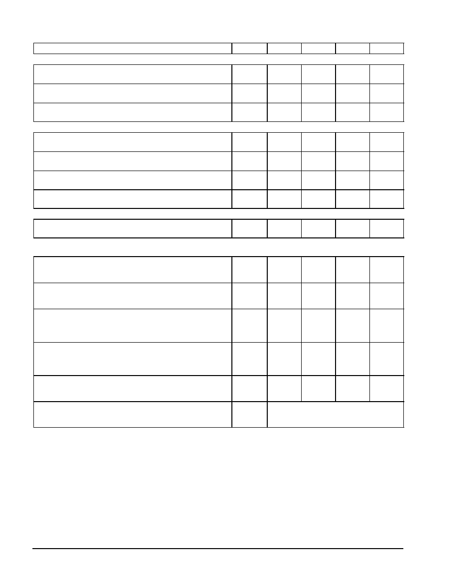
ELECTRICAL CHARACTERISTICS
(T
C
= 25∞C unless otherwise noted)
Characteristic
Symbol
Min
Typ
Max
Unit
OFF CHARACTERISTICS
Drain-Source Breakdown Voltage
(V
GS
= 0 Vdc, I
D
= 100 µAdc)
V
(BR)DSS
65
--
--
Vdc
Zero Gate Voltage Drain Current
(V
DS
= 28 Vdc, V
GS
= 0 Vdc)
I
DSS
--
--
10
µAdc
Gate-Source Leakage Current
(V
GS
= 5 Vdc, V
DS
= 0 Vdc)
I
GSS
--
--
1
µAdc
ON CHARACTERISTICS (DC)
Gate Threshold Voltage
(V
DS
= 10 Vdc, I
D
= 100 µAdc)
V
GS(th)
2
--
4
Vdc
Gate Quiescent Voltage
(V
DS
= 28 Vdc, I
D
= 500 mAdc)
V
GS(Q)
3
3.9
5
Vdc
Drain-Source On-Voltage
(V
GS
= 10 Vdc, I
D
= 1 Adc)
V
DS(on)
--
0.19
0.21
Vdc
Forward Transconductance
(V
DS
= 10 Vdc, I
D
= 1 Adc)
g
fs
--
3
--
S
DYNAMIC CHARACTERISTICS (1)
Reverse Transfer Capacitance
(V
DS
= 28 Vdc, V
GS
= 0, f = 1 MHz)
C
rss
--
1.8
--
pF
FUNCTIONAL TESTS (In Motorola Test Fixture, 50 ohm system) 2-carrier W-CDMA. Peak/Avg. ratio = 8.3 dB @ 0.01% Probability
on CCDF.
Common-Source Amplifier Power Gain
(V
DD
= 28 Vdc, P
out
= 10 W Avg., I
DQ
= 500 mA, f1 = 2112.5 MHz,
f2 = 2122.5 MHz and f1 = 2157.5 MHz, f2 = 2167.5 MHz)
G
ps
13.5
15
--
dB
Drain Efficiency
(V
DD
= 28 Vdc, P
out
= 10 W Avg., I
DQ
= 500 mA, f1 = 2112.5 MHz,
f2 = 2122.5 MHz and f1 = 2157.5 MHz, f2 = 2167.5 MHz)
21
23.5
--
%
Third Order Intermodulation Distortion
(V
DD
= 28 Vdc, P
out
= 10 W Avg., I
DQ
= 500 mA, f1 = 2112.5 MHz,
f2 = 2122.5 MHz and f1 = 2157.5 MHz, f2 = 2167.5 MHz; IM3
measured over 3.84 MHz Bandwidth at f1 -10 MHz and f2 +10 MHz.)
IM3
--
-37.5
-35
dBc
Adjacent Channel Power Ratio
(V
DD
= 28 Vdc, P
out
= 10 W Avg., I
DQ
= 500 mA, f1 = 2112.5 MHz,
f2 = 2122.5 MHz and f1 = 2157.5 MHz, f2 = 2167.5 MHz; ACPR
measured over 3.84 MHz Bandwidth at f1 -5 MHz and f2 +5 MHz.)
ACPR
--
-41
-38
dBc
Input Return Loss
(V
DD
= 28 Vdc, P
out
= 10 W Avg., I
DQ
= 500 mA, f1 = 2112.5 MHz,
f2 = 2122.5 MHz and f1 = 2157.5 MHz, f2 = 2167.5 MHz)
IRL
--
-12
-9
dB
Output Mismatch Stress
(V
DD
= 28 Vdc, P
out
= 45 W CW, I
DQ
= 500 mA, f = 2170 MHz
VSWR = 5:1, All Phase Angles at Frequency of Tests)
No Degradation In Output Power
Before and After Test
(1) Part is internally matched both on input and output.
F
r
e
e
s
c
a
l
e
S
e
m
i
c
o
n
d
u
c
t
o
r
,
I
Freescale Semiconductor, Inc.
For More Information On This Product,
Go to: www.freescale.com
n
c
.
.
.

3
MRF21045LR3 MRF21045LSR3
MOTOROLA RF DEVICE DATA
ELECTRICAL CHARACTERISTICS -- continued
(T
C
= 25∞C unless otherwise noted)
Characteristic
Unit
Max
Typ
Min
Symbol
FUNCTIONAL TESTS (In Motorola Test Fixture, 50 ohm system) -- continued
Two-Tone Common-Source Amplifier Power Gain
(V
DD
= 28 Vdc, P
out
= 45 W PEP, I
DQ
= 500 mA,
f1 = 2110 MHz, f2 = 2120 MHz and f1 = 2160 MHz, f2 = 2170 MHz)
G
ps
--
14.9
--
dB
Two-Tone Drain Efficiency
(V
DD
= 28 Vdc, P
out
= 45 W PEP, I
DQ
= 500 mA,
f1 = 2110 MHz, f2 = 2120 MHz and f1 = 2160 MHz, f2 = 2170 MHz)
--
36
--
%
Intermodulation Distortion
(V
DD
= 28 Vdc, P
out
= 45 W PEP, I
DQ
= 500 mA,
f1 = 2110 MHz, f2 = 2120 MHz and f1 = 2160 MHz, f2 = 2170 MHz)
IMD
--
-30
--
dBc
Two-Tone Input Return Loss
(V
DD
= 28 Vdc, P
out
= 45 W PEP, I
DQ
= 500 mA,
f1 = 2110 MHz, f2 = 2120 MHz and f1 = 2160 MHz, f2 = 2170 MHz)
IRL
--
-12
--
dB
P
out
, 1 dB Compression Point
(V
DD
= 28 Vdc, I
DQ
= 500 mA, f = 2170 MHz)
P1dB
--
50
--
W
F
r
e
e
s
c
a
l
e
S
e
m
i
c
o
n
d
u
c
t
o
r
,
I
Freescale Semiconductor, Inc.
For More Information On This Product,
Go to: www.freescale.com
n
c
.
.
.
MRF21045LR3 MRF21045LSR3
4
MOTOROLA RF DEVICE DATA
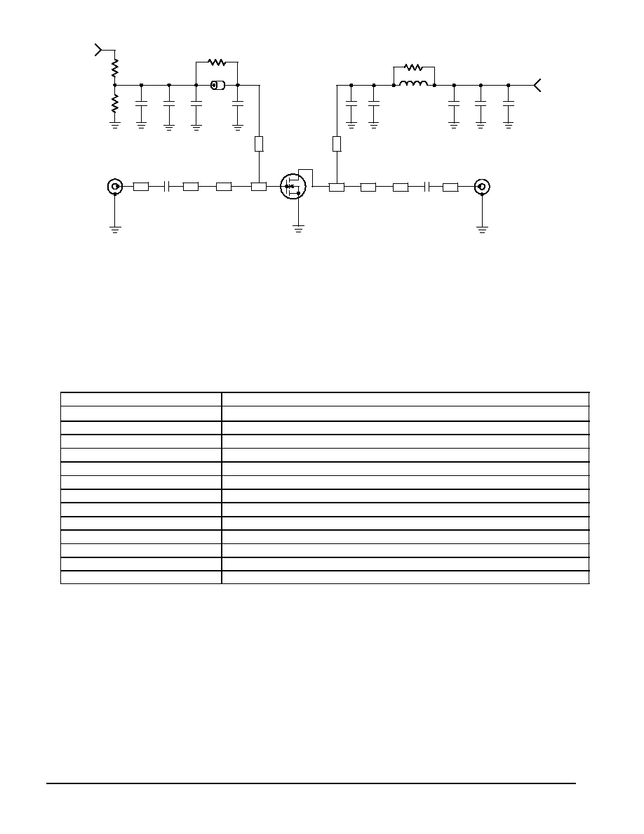
Figure 1. MRF21045LR3(LSR3) Test Circuit Schematic
RF
INPUT
RF
OUTPUT
Z1
Z2
V
GG
C1
C6
L1
DUT
V
DD
Z4
C8
Z9
C5
C7
Z6
Z7
R4
C4
Z5
+
C9
C3
C2
Z10
C10
C11
+
+
B1
R1
R2
R3
Board
0.030 Glass Teflon
,
Keene GX-0300-55-22,
r
= 2.55
PCB
Etched Circuit Boards
MRF21045 Rev. 3, CMR
Z1, Z9
0.750 x 0.084 Transmission Line
Z2
0.160 x 0.084 Transmission Line
Z3
1.195 x 0.176 Transmission Line
Z4
0.125 x 0.320 Transmission Line
Z5
1.100 x 0.045 Transmission Line
Z6
0.442 x 0.650 Transmission Line
Z7
0.490 x 0.140 Transmission Line
Z8
0.540 x 0.084 Transmission Line
Z10
0.825 x 0.055 Transmission Line
Z3
Z8
Table 1. MRF21045LR3(LSR3) Component Designations and Values
Designators
Description
B1
Short Ferrite Bead, Fair Rite, #2743019447
C1, C2, C6
43 pF Chip Capacitors, ATC #100B430JCA500X
C7
5.6 pF Chip Capacitor, ATC #100B5R6JCA500X
C3, C9
1000 pF Chip Capacitors, ATC #100B102JCA500X
C4, C10
0.1 mF Chip Capacitors, Kemet #CDR33BX104AKWS
C5
1.0 mF Tantalum Chip Capacitor, Kemet #T491C105M050
C8
10 mF Tantalum Chip Capacitor, Kemet #T495X106K035AS4394
C11
22 mF Tantalum Chip Capacitor, Kemet #T491X226K035AS4394
L1
1 Turn, #20 AWG, 0.100 ID, Motorola
N1, N2
Type N Flange Mounts, Omni Spectra #3052-1648-10
R1
1.0 k, 1/8 W Chip Resistor
R2
180 k, 1/8 W Chip Resistor
R3, R4
10 , 1/8 W Chip Resistors
F
r
e
e
s
c
a
l
e
S
e
m
i
c
o
n
d
u
c
t
o
r
,
I
Freescale Semiconductor, Inc.
For More Information On This Product,
Go to: www.freescale.com
n
c
.
.
.
5
MRF21045LR3 MRF21045LSR3
MOTOROLA RF DEVICE DATA
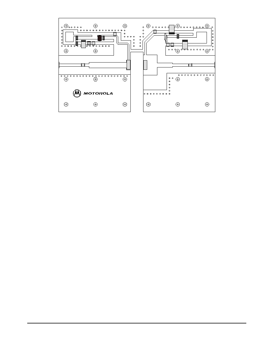
Figure 2. MRF21045LR3(LSR3) Test Circuit Component Layout
MRF21045
C1
WB1
WB2
C3
C5
C4
R2
R1
R3
B1
C2
C6
C8
C7
C11
L1
C9
R4
C10
F
r
e
e
s
c
a
l
e
S
e
m
i
c
o
n
d
u
c
t
o
r
,
I
Freescale Semiconductor, Inc.
For More Information On This Product,
Go to: www.freescale.com
n
c
.
.
.