 | –≠–ª–µ–∫—Ç—Ä–æ–Ω–Ω—ã–π –∫–æ–º–ø–æ–Ω–µ–Ω—Ç: MRF21090 | –°–∫–∞—á–∞—Ç—å:  PDF PDF  ZIP ZIP |
1
MRF21090R3 MRF21090SR3
MOTOROLA RF DEVICE DATA
The RF Sub-Micron MOSFET Line
RF Power Field Effect Transistors
N-Channel Enhancement-Mode Lateral MOSFETs
Designed for W-CDMA base station applications with frequencies from 2110
to 2170 MHz. Suitable for FM, TDMA, CDMA and multicarrier amplifier
applications.
∑ Typical W-CDMA Performance for 2140 MHz, 28 Volts
4.096 MHz BW @ 5 MHz offset, 1 PERCH 15 DTCH:
Output Power -- 11.5 Watts
Efficiency -- 16%
Gain -- 12.2 dB
ACPR -- -45 dBc
∑ Internally Matched, Controlled Q, for Ease of Use
∑ High Gain, High Efficiency and High Linearity
∑ Integrated ESD Protection
∑ Designed for Maximum Gain and Insertion Phase Flatness
∑ Capable of Handling 10:1 VSWR, @ 28 Vdc, 2110 MHz, 90 Watts CW
Output Power
∑ Excellent Thermal Stability
∑ Characterized with Series Equivalent Large-Signal Impedance Parameters
∑ In Tape and Reel. R3 Suffix = 250 Units per 56 mm, 13 inch Reel.
MAXIMUM RATINGS
Rating
Symbol
Value
Unit
Drain-Source Voltage
V
DSS
65
Vdc
Gate-Source Voltage
V
GS
+15, -0.5
Vdc
Total Device Dissipation @ T
C
= 25∞C
Derate above 25∞C
P
D
270
1.54
Watts
W/∞C
Storage Temperature Range
T
stg
- 65 to +150
∞C
Operating Junction Temperature
T
J
200
∞C
THERMAL CHARACTERISTICS
Characteristic
Symbol
Value
Unit
Thermal Resistance, Junction to Case
R
JC
0.65
∞C/W
NOTE - CAUTION - MOS devices are susceptible to damage from electrostatic charge. Reasonable precautions in handling and
packaging MOS devices should be observed.
Order this document
by MRF21090/D
MOTOROLA
SEMICONDUCTOR TECHNICAL DATA
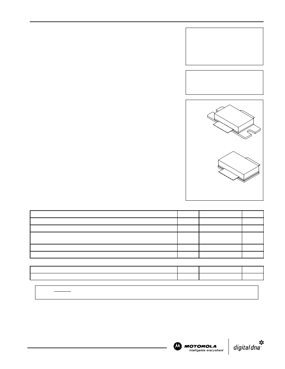
MRF21090R3
MRF21090SR3
2170 MHz, 90 W, 28 V
LATERAL N-CHANNEL
RF POWER MOSFETs
CASE 465C-02, STYLE 1
NI-880S
MRF21090SR3
CASE 465B-03, STYLE 1
NI-880
MRF21090R3
Motorola, Inc. 2004
REV 6
F
r
e
e
s
c
a
l
e
S
e
m
i
c
o
n
d
u
c
t
o
r
,
I
Freescale Semiconductor, Inc.
For More Information On This Product,
Go to: www.freescale.com
n
c
.
.
.
MRF21090R3 MRF21090SR3
2
MOTOROLA RF DEVICE DATA
ESD PROTECTION CHARACTERISTICS
Test Conditions
Class
Human Body Model
MRF21090R3
MRF21090SR3
2 (Minimum)
1 (Minimum)
Machine Model
MRF21090R3
MRF21090SR3
M3 (Minimum)
M4 (Minimum)
ELECTRICAL CHARACTERISTICS
(T
C
= 25∞C unless otherwise noted)
Characteristic
Symbol
Min
Typ
Max
Unit
OFF CHARACTERISTICS
Drain-Source Breakdown Voltage
(V
GS
= 0 Vdc, I
D
= 100 µAdc)
V
(BR)DSS
65
--
--
Vdc
Gate-Source Leakage Current
(V
GS
= 5 Vdc, V
DS
= 0 Vdc)
I
GSS
--
--
1
µAdc
Zero Gate Voltage Drain Leakage Current
(V
DS
= 28 Vdc, V
GS
= 0 Vdc)
I
DSS
--
--
10
µAdc
ON CHARACTERISTICS
Forward Transconductance
(V
DS
= 10 Vdc, I
D
= 3 Adc)
g
fs
--
7.2
--
S
Gate Threshold Voltage
(V
DS
= 10 V, I
D
= 300 µA)
V
GS(th)
2
3
4
Vdc
Gate Quiescent Voltage
(V
DS
= 28 V, I
D
= 750 mA)
V
GS(Q)
3
3.8
5
Vdc
Drain-Source On-Voltage
(V
GS
= 10 V, I
D
= 1 A)
V
DS(on)
--
0.1
0.6
Vdc
DYNAMIC CHARACTERISTICS
Reverse Transfer Capacitance (1)
(V
DS
= 28 Vdc, V
GS
= 0, f = 1 MHz)
C
rss
--
4.2
--
pF
FUNCTIONAL TESTS (In Motorola Test Fixture)
Common-Source Amplifier Power Gain
(V
DD
= 28 Vdc, P
out
= 90 W PEP, I
DQ
= 750 mA, f1 = 2110.0 MHz,
f2 = 2110.1 MHz and f1 = 2170.0 MHz, f2 = 2170.1 MHz)
G
ps
10
11.7
--
dB
Drain Efficiency
(V
DD
= 28 Vdc, P
out
= 90 W PEP, I
DQ
= 750 mA, f1 = 2110.0 MHz,
f2 = 2110.1 MHz and f1 = 2170.0 MHz, f2 = 2170.1 MHz)
30
33
--
%
Intermodulation Distortion
(V
DD
= 28 Vdc, P
out
= 90 W PEP, I
DQ
= 750 mA, f1 = 2110.0 MHz,
f2 = 2110.1 MHz and f1 = 2170.0 MHz, f2 = 2170.1 MHz)
IMD
--
-30
-27.5
dBc
Input Return Loss
(V
DD
= 28 Vdc, P
out
= 90 W PEP, I
DQ
= 750 mA, f1 = 2110.0 MHz,
f2 = 2110.1 MHz and f1 = 2170.0 MHz, f2 = 2170.1 MHz)
IRL
--
-12
-9.0
dB
Common-Source Amplifier Power Gain
(V
DD
= 28 Vdc, P
out
= 75 W CW, I
DQ
= 750 mA, f = 2170 MHz)
G
ps
--
11.7
--
dB
Drain Efficiency
(V
DD
= 28 Vdc, P
out
= 75 W CW, I
DQ
= 750 mA, f = 2170 MHz)
--
41
--
%
Output Mismatch Stress
(V
DD
= 28 Vdc, P
out
= 90 W CW, I
DQ
= 750 mA, f = 2110 MHz,
VSWR = 10:1, All Phase Angles at Frequency of Tests)
No Degradation In Output Power
Before and After Test
(1) Part is internally matched both on input and output.
F
r
e
e
s
c
a
l
e
S
e
m
i
c
o
n
d
u
c
t
o
r
,
I
Freescale Semiconductor, Inc.
For More Information On This Product,
Go to: www.freescale.com
n
c
.
.
.
3
MRF21090R3 MRF21090SR3
MOTOROLA RF DEVICE DATA
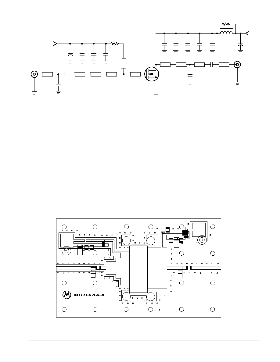
Figure 1. MRF21090R3(SR3) Test Circuit Schematic
B1
Ferrite Bead, Fair Rite #2743019447
C1, C13
470 µF, 50 V Electrolytic Capacitors
C2, C10
22 µF, 35 V Tantalum Surface Mount Chip
Capacitors, Kemet
C3, C9
20 nF Chip Capacitors, ATC #100B203MCA500X
C4, C8
5.1 pF Chip Capacitors, ATC #100B5R1CCA500X
C5, C12
0.4 - 2.5 pF Variable Capacitors, Johanson Gigatrim
C6
10 pF Chip Capacitor, ATC #100B100JCA500X
C7
1 mF, 35 V Tantalum Surface Mount Chip Capacitor,
Kemet
C11
1 nF Chip Capacitor, ATC #100B102JCA500X
C14
8.2 pF Chip Capacitor, ATC #100B8R2CCA500X
R1
13 , 1/4 W Chip Resistor,
Garret Instrument #RM73B2B130JT,
R2
12 , 1/4 W Chip Resistor,
Garret Instrument #RM73B2B120JT
Z1
30.7 x 2.09 mm Microstrip
Z2
5.99 x 2.09 mm Microstrip
Z3
7.55 x 9.89 mm Microstrip
Z4
3.77 x 15.71 mm Microstrip
Z5
6.89 x 26.17 mm Microstrip
Z6
14.93 x 32.05 mm Microstrip
V
V
RF INPUT
RF OUTPUT
R1
Z1
Z2
Z3
Z4
Z5
Z6
Z7
Z8
Z9
Z10
Z11
C7
C8
C9
C10
C11
C12
C14
C13
C6
R2
B1
DUT
C5
C1
C2
C3
C4
GG
DD
Z7
10.23 x 2.09 mm Microstrip
Z8
6.03 x 2.09 mm Microstrip
Z9
23.98 x 2.09 mm Microstrip
Z10
29.82 x 1.15 mm Microstrip
Z11
17.08 x 1.15 mm Microstrip
WS1, WS2
Beryllium Copper Wear Blocks 5 mils Thick
Brass Banana Jack and Nut
Red Banana Jack and Nut
Green Banana Jack and Nut
Type N Jack Connectors, 3052-1648-10,
Omni Specra
4-40 Head Screws 0.125 Long
4-40 Head Screws 0.188 Long
4-40 Head Screws 0.312 Long
4-40 Head Screws 0.438 Long
Endplates Brass Endplates for Copper Bedstead
Bedstead
Copper Bedstead/Heatsink
Insert
Copper Bedstead Insert
Raw PCB
0.030 Glass Teflon
, 2 oz Copper Clad
3 x 5 Arion
RF Circuit
3 x 5 Copper Clad PCB Teflon
,
MRF21090, CMR
+
+
+
+
+
Figure 2. MRF21090R3(SR3) Test Circuit Component Layout
C
U
T
O
U
T
Drain
Feed
C1
C2
C3 C4
C6
C5
C7 C8
C9
C10
C11
C12
C14
B1
R2
R1
C13
Bias
Gate
Feed
Bias
MRF21090
F
r
e
e
s
c
a
l
e
S
e
m
i
c
o
n
d
u
c
t
o
r
,
I
Freescale Semiconductor, Inc.
For More Information On This Product,
Go to: www.freescale.com
n
c
.
.
.

MRF21090R3 MRF21090SR3
4
MOTOROLA RF DEVICE DATA
TYPICAL PERFORMANCE (IN MOTOROLA TEST FIXTURE)
P
out
, OUTPUT POWER (WATTS) AVG.
f, FREQUENCY (MHz)
60
0
Figure 3. Class AB Broadband Circuit
Performance
2080
10
5
Figure 4. CDMA ACPR, Power Gain and Drain
Efficiency versus Output Power
20
0
30
20
15
20
30
40
V
DD
= 28 Vdc
P
out
= 90 W (PEP)
I
DQ
= 750 mA
Two-Tone Measurement
100 kHz Tone Spacing
Figure 5. Intermodulation Distortion versus
Output Power
Figure 6. Intermodulation Distortion Products
versus Output Power
10
25
P
out
, OUTPUT POWER (WATTS) PEP
-25
-55
1
-45
-40
-30
100
IMD, INTERMODULA
TION
DIST
ORTION
(dBc)
-50
-35
10
Figure 7. Power Gain versus Output Power
Figure 8. Power Gain and Intermodulation
Distortion versus Supply Voltage
P
out
, OUTPUT POWER (WATTS) PEP
15
10
1
12
14
100
G
ps
, POWER GAIN (dB)
11
13
V
DS
, DRAIN VOLTAGE (VOLTS)
11.8
11.0
11.4
11.6
34
20
22
28
10.8
11.2
10.6
10
32
24
26
30
2100
2120
2140
2160
2180
2200
50
-35
-30
-25
-20
-15
-10
-5
5.0
10
15
-70
-60
-50
-40
-30
-20
ADJACENT
CHANNEL
POWER RA
TIO
(
dB
)
V
DD
= 28 Vdc
f = 2140 MHz
Two-Tone Measurement
100 kHz Tone Spacing
P
out
, OUTPUT POWER (WATTS) PEP
-20
-80
1
-60
-50
-30
100
IMD, INTERMODULA
TION
DIST
ORTION
(dBc)
-70
-40
10
V
DD
= 28 Vdc
I
DQ
= 750 mA
f = 2140 MHz
Two-Tone Measurement
100 kHz Tone Spacing
G
ps
, POWER GAIN (dB)
IMD, INTERMODULA
TION
DIST
ORTION
(dBc)
-34
-32
-30
-28
-26
-24
-22
V
DD
= 28 Vdc
f = 2140 MHz
Two-Tone Measurement
100 kHz Tone Spacing
P
out
= 90 W (PEP)
I
DQ
= 750 mA
f = 2140 MHz
Two-Tone Measurement
100 kHz Tone Spacing
Fixture Tuned for 28 Volts
IRL
G
ps
IMD
ACPR
1000 mA
800 mA
1500 mA
500 mA
2000 mA
5th Order
7th Order
3rd Order
2000 mA
1500 mA
1000 mA
800 mA
500 mA
IMD
, DRAIN EFFICIENCY
(%),
G
ps
, POWER GAIN (dB
)
, DRAIN EFFICIENCY
(%),
G
ps
, POWER GAIN (dB
)
IRL,
INPUT
RETURN LOSS (dB)
IMD, INTERMODULA
TION
DIST
ORTION
(dBc)
G
ps
G
ps
V
DD
= 28 Vdc
I
DQ
= 1000 mA
f = 2140 MHz
Channel Spacing (Channel Bandwidth):
4.096 MHz (5 MHz)
F
r
e
e
s
c
a
l
e
S
e
m
i
c
o
n
d
u
c
t
o
r
,
I
Freescale Semiconductor, Inc.
For More Information On This Product,
Go to: www.freescale.com
n
c
.
.
.

5
MRF21090R3 MRF21090SR3
MOTOROLA RF DEVICE DATA
Figure 9. Series Equivalent Source and Load Impedance
f
MHz
Z
source
Z
load
2110
2140
2170
3.03 - j3.40
2.60 - j3.50
3.02 - j3.46
0.92 - j1.67
0.97 - j1.80
0.90 - j1.52
V
DD
= 28 V, I
DQ
= 750 mA, P
out
= 90 W (PEP)
2110 MHz
f = 2170 MHz
f = 2110 MHz
2170 MHz
Z
source
= Test circuit impedance as measured from
gate to ground.
Z
load
= Test circuit impedance as measured
from drain to ground.
Z source
Z load
Input
Matching
Network
Device
Under Test
Output
Matching
Network
Z
source
Z
load
Z
o
= 5
F
r
e
e
s
c
a
l
e
S
e
m
i
c
o
n
d
u
c
t
o
r
,
I
Freescale Semiconductor, Inc.
For More Information On This Product,
Go to: www.freescale.com
n
c
.
.
.