
5-393
FAST AND LS TTL DATA
QUAD BUS TRANSCEIVER
The SN54/ 74LS242 and SN54 / 74LS243 are Quad Bus Transmitters / Re-
ceivers designed for 4-line asynchronous 2-way data communications
between data buses.
∑
Hysteresis at Inputs to Improve Noise Immunity
∑
2-Way Asynchronous Data Bus Communication
∑
Input Clamp Diodes Limit High-Speed Termination Effects
LOGIC AND CONNECTION DIAGRAMS DIP (TOP VIEW)
14
13
12
11
10
9
1
2
3
4
5
6
8
7
VCC GBA NC
1B
2B
3B
4B
GBA
NC
1A
2A
3A
4A
GND
SN54 / 74LS242
SN54 / 74LS243
14
13
12
11
10
9
1
2
3
4
5
6
8
7
VCC GBA NC
1B
2B
3B
4B
GBA
NC
1A
2A
3A
4A
GND
NOTE:
The Flatpak version
has the same pinouts
(Connection Diagram) as
the Dual In-Line Package.
TRUTH TABLES
SN54 / 74LS242
INPUTS
OUTPUT
INPUTS
OUTPUT
GAB
D
OUTPUT
GAB
D
OUTPUT
L
L
H
L
X
(Z)
L
H
L
H
L
H
H
X
(Z)
H
H
L
SN54/74LS243
INPUTS
OUTPUT
INPUTS
OUTPUT
GAB
D
OUTPUT
GAB
D
OUTPUT
L
L
L
L
X
(Z)
L
H
H
H
L
H
H
X
(Z)
H
H
L
H = HIGH Voltage Level
L = LOW Voltage Level
X = Immaterial
Z = HIGH Impedance
SN54/74LS242
SN54/74LS243
QUAD BUS TRANSCEIVER
LOW POWER SCHOTTKY
ORDERING INFORMATION
SN54LSXXXJ
Ceramic
SN74LSXXXN
Plastic
SN74LSXXXDW SOIC
J SUFFIX
CERAMIC
CASE 632-08
N SUFFIX
PLASTIC
CASE 646-06
14
1
14
1
14
1
D SUFFIX
SOIC
CASE 751A-02

5-394
FAST AND LS TTL DATA
SN54/74LS242
∑
SN54/74LS243
GUARANTEED OPERATING RANGES
Symbol
Parameter
Min
Typ
Max
Unit
VCC
Supply Voltage
54
74
4.5
4.75
5.0
5.0
5.5
5.25
V
TA
Operating Ambient Temperature Range
54
74
≠ 55
0
25
25
125
70
∞
C
IOH
Output Current -- High
54, 74
≠ 3.0
mA
OH
54
74
≠ 12
≠ 15
mA
IOL
Output Current -- Low
54
74
12
24
mA
DC CHARACTERISTICS OVER OPERATING TEMPERATURE RANGE
(unless otherwise specified)
Symbol
Parameter
Limits
Unit
Test Conditions
Symbol
Parameter
Min
Typ
Max
Unit
Test Conditions
VIH
Input HIGH Voltage
2.0
V
Guaranteed Input HIGH Voltage for
All Inputs
VIL
Input LOW Voltage
54
0.7
V
Guaranteed Input LOW Voltage for
All Inputs
VIL
Input LOW Voltage
74
0.8
V
Guaranteed Input LOW Voltage for
All Inputs
VT+≠VT≠
Hysteresis
0.2
0.4
V
VCC = MIN
VIK
Input Clamp Diode Voltage
≠ 0.65
≠ 1.5
V
VCC = MIN, IIN = ≠ 18 mA
VOH
Output HIGH Voltage
54, 74
2.4
3.4
V
VCC = MIN, IOH = ≠ 3.0 mA
VOH
Output HIGH Voltage
54, 74
2.0
V
VCC = MIN, IOH = MAX
VOL
Output LOW Voltage
54, 74
0.25
0.4
V
IOL = 12 mA
VCC = VCC MIN,
VIN = VIL or VIH
per Truth Table
VOL
Output LOW Voltage
74
0.35
0.5
V
IOL = 24 mA
VIN = VIL or VIH
per Truth Table
IOZH
Output Off Current HIGH
40
µ
A
VCC = MAX, VOUT = 2.7 V
IOZL
Output Off Current LOW
≠ 200
µ
A
VCC = MAX, VOUT = 0.4 V
IIH
Input HIGH Current
D, E1, E2
20
µ
A
VCC = MAX, VIN = 2.7 V
IIH
Input HIGH Current
E1, E2
0.1
mA
VCC = MAX, VIN = 7.0 V
IH
D Input
0.1
mA
VCC = MAX, VIN = 5.5 V
IIL
Input LOW Current
≠ 0.2
mA
VCC = MAX, VIN = 0.4 V
IOS
Output Short Circuit Current (Note 1)
≠ 40
≠ 225
mA
VCC = MAX
ICC
Power Supply Current
Total, Output HIGH
38
mA
VCC = MAX
ICC
Total, Output LOW
50
mA
VCC = MAX
ICC
Total at HIGH Z
LS242
50
mA
VCC = MAX
Total at HIGH Z
LS243
54
Note 1: Not more than one output should be shorted at a time, nor for more than 1 second.
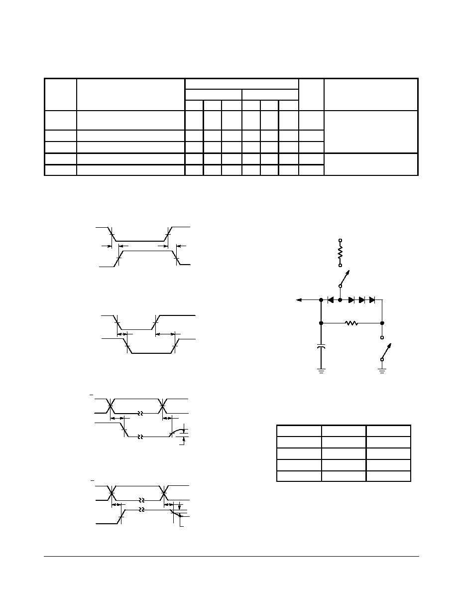
AC WAVEFORMS
1.3 V
1.3 V
1.3 V
1.3 V
1.3 V
1.3 V
1.3 V
VIN
VOUT
tPLH
tPHL
1.3 V
1.3 V
VIN
VOUT
SW2
CL*
5 k
SW1
VCC
RL
TO OUTPUT
UNDER TEST
1.3 V
tPHL
tPLH
VE
VE
VOUT
VE
VE
VOUT
tPHZ
1.3 V
1.3 V
tPZL
tPLZ
VOL
1.3 V
VOH
0.5 V
tPZH
1.3 V
Figure 1
Figure 2
Figure 3
Figure 4
Figure 5
1.3 V
0.5 V
1.3 V
SWITCH POSITIONS
5-395
FAST AND LS TTL DATA
SN54/74LS242
∑
SN54/74LS243
AC CHARACTERISTICS
(TA = 25
∞
C, VCC = 5.0 V)
Symbol
Parameter
Limits
Unit
Test Conditions
Symbol
Parameter
LS242
LS243
Unit
Test Conditions
Symbol
Parameter
Min
Typ
Max
Min
Typ
Max
Unit
Test Conditions
tPLH
tPHL
Propagation Delay, Data to Output
9.0
12
14
18
12
12
18
18
ns
CL = 45 pF,
RL = 667
tPZH
Output Enable Time to HIGH Level
15
23
15
23
ns
CL = 45 pF,
RL = 667
tPZL
Output Enable Time to LOW Level
20
30
20
30
ns
tPLZ
Output Disable Time from LOW Level
15
25
15
25
ns
CL = 5.0 pF,
RL = 667
tPHZ
Output Disable Time from HIGH Level
10
18
10
18
ns
CL = 5.0 pF,
RL = 667
SYMBOL
SW1
SW2
tPZH
Open
Closed
tPZL
Closed
Open
tPLZ
Closed
Closed
tPHZ
Closed
Closed

5-396
FAST AND LS TTL DATA
MIN
MIN
MAX
MAX
MILLIMETERS
INCHES
DIM
A
B
C
D
F
G
J
K
M
P
R
8.55
3.80
1.35
0.35
0.40
0.19
0.10
0
∞
5.80
0.25
8.75
4.00
1.75
0.49
1.25
0.25
0.25
7
∞
6.20
0.50
0.337
0.150
0.054
0.014
0.016
0.008
0.004
0
∞
0.229
0.010
0.344
0.157
0.068
0.019
0.049
0.009
0.009
7
∞
0.244
0.019
1.27 BSC
0.050 BSC
NOTES:
1. DIMENSIONS A" AND B" ARE DATUMS AND
T" IS A DATUM SURFACE.
2. DIMENSIONING AND TOLERANCING PER ANSI
Y14.5M, 1982.
3. CONTROLLING DIMENSION: MILLIMETER.
4. DIMENSION A AND B DO NOT INCLUDE MOLD
PROTRUSION.
5. MAXIMUM MOLD PROTRUSION 0.15 (0.006)
PER SIDE.
6. 751A 01 IS OBSOLETE, NEW STANDARD
751A 02.
-A-
-B-
P
G
C
K
SEATING
PLANE
14 PL
D
M
F
J
7 PL
R X 45
∞
1
7
8
14
Case 751A-02 D Suffix
14-Pin Plastic
SO-14
B
0.25 (0.010)
M
M
T
0.25 (0.010)
B
A
M
S
S
Case 632-08 J Suffix
14-Pin Ceramic Dual In-Line
MIN
MIN
MAX
MAX
MILLIMETERS
INCHES
DIM
A
B
C
D
F
G
J
K
L
M
N
19.05
6.23
3.94
0.39
1.40
0.21
3.18
0
∞
0.51
19.94
7.11
5.08
0.50
1.65
0.38
4.31
15
∞
1.01
0.750
0.245
0.155
0.015
0.055
0.008
0.125
0
∞
0.020
0.785
0.280
0.200
0.020
0.065
0.015
0.170
15
∞
0.040
2.54 BSC
7.62 BSC
0.100 BSC
0.300 BSC
NOTES:
1. DIMENSIONING AND TOLERANCING PER ANSI
Y14.5M, 1982.
2. CONTROLLING DIMENSION: INCH.
3. DIMENSION L TO CENTER OF LEAD WHEN
FORMED PARALLEL.
4. DIM F MAY NARROW TO 0.76 (0.030) WHERE
THE LEAD ENTERS THE CERAMIC BODY.
5. 632 01 THRU 07 OBSOLETE, NEW STANDARD
632 08.
14
8
1
7
-A-
-B-
-T-
SEATING
PLANE
F
G
D
14 PL
N
K
C
L
J
14 PL
M
0.25 (0.010)
T A
M
S
0.25 (0.010)
T B
M
S
Case 646-06 N Suffix
14-Pin Plastic
MIN
MIN
MAX
MAX
MILLIMETERS
INCHES
DIM
18.16
6.10
3.69
0.38
1.02
1.32
0.20
2.92
19.56
6.60
4.69
0.53
1.78
2.41
0.38
3.43
0
∞
0.39
0.715
0.240
0.145
0.015
0.040
0.052
0.008
0.115
0.770
0.260
0.185
0.021
0.070
0.095
0.015
0.135
10
∞
1.01
2.54 BSC
7.62 BSC
0.100 BSC
0.300 BSC
0
∞
0.015
10
∞
0.039
A
B
C
D
F
G
H
J
K
L
M
N
NOTES:
1. LEADS WITHIN 0.13 mm (0.005) RADIUS OF TRUE
POSITION AT SEATING PLANE AT MAXIMUM
MATERIAL CONDITION.
2. DIMENSION L" TO CENTER OF LEADS WHEN
FORMED PARALLEL.
3. DIMENSION B" DOES NOT INCLUDE MOLD
FLASH.
4. ROUNDED CORNERS OPTIONAL.
5. 646 05 OBSOLETE, NEW STANDARD 646 06.
1
7
14
8
B
A
NOTE 4
F
H
G
D
SEATING
PLANE
N
K
C
L
J
M

5-397
FAST AND LS TTL DATA
Motorola reserves the right to make changes without further notice to any products herein. Motorola makes no warranty, representation or guarantee regarding
the suitability of its products for any particular purpose, nor does Motorola assume any liability arising out of the application or use of any product or circuit,
and specifically disclaims any and all liability, including without limitation consequential or incidental damages. "Typical" parameters can and do vary in different
applications. All operating parameters, including "Typicals" must be validated for each customer application by customer's technical experts. Motorola does
not convey any license under its patent rights nor the rights of others. Motorola products are not designed, intended, or authorized for use as components in
systems intended for surgical implant into the body, or other applications intended to support or sustain life, or for any other application in which the failure of
the Motorola product could create a situation where personal injury or death may occur. Should Buyer purchase or use Motorola products for any such
unintended or unauthorized application, Buyer shall indemnify and hold Motorola and its officers, employees, subsidiaries, affiliates, and distributors harmless
against all claims, costs, damages, and expenses, and reasonable attorney fees arising out of, directly or indirectly, any claim of personal injury or death
associated with such unintended or unauthorized use, even if such claim alleges that Motorola was negligent regarding the design or manufacture of the part.
Motorola and
are registered trademarks of Motorola, Inc. Motorola, Inc. is an Equal Opportunity/Affirmative Action Employer.
Literature Distribution Centers:
USA: Motorola Literature Distribution; P.O. Box 20912; Phoenix, Arizona 85036.
EUROPE: Motorola Ltd.; European Literature Centre; 88 Tanners Drive, Blakelands, Milton Keynes, MK14 5BP, England.
JAPAN: Nippon Motorola Ltd.; 4-32-1, Nishi-Gotanda, Shinagawa-ku, Tokyo 141, Japan.
ASIA PACIFIC: Motorola Semiconductors H.K. Ltd.; Silicon Harbour Center, No. 2 Dai King Street, Tai Po Industrial Estate, Tai Po, N.T., Hong Kong.