
NEC's 4 PIN SOP PACKAGE,
HIGH ISOLATION VOLTAGE,
3000 V.r.m.s. 1 FORM A TYPE
SOLID STATE RELAY
PS7431-1A
FEATURES
∑ HIGH ISOLATION VOLTAGE:
BV: 3000 V
r.m.s.
MIN
∑
SMALL AND THIN PACKAGE:
4-pin SOP, Height = 2.1 mm
∑ 1 FORM A OUTPUT
∑ LOW OPERATING CURRENT:
I
F
2 mA MIN
∑ DESIGNED FOR AC/DC SWITCHING LINE CHANGER
∑ LOW OFFSET VOLTAGE
∑ AVAILABLE IN TAPE AND REEL:
PS7431-1A-E3, E4, F3, F4
DESCRIPTION
NEC's PS7431-1A is a solid state relay containing GaAs LEDs
on the input side and 1 form, normally open (N.O.) contact
MOS FETs on the output side.
APPLICATIONS
∑ LAPTOP, PC, PDA
∑ MODEM CARD
∑ TELEPHONE, FAX
∑ MEASUREMENT EQUIPMENT
ELECTRICAL CHARACTERISTICS
(T
A
= 25
į
C)
SYMBOLS
PARAMETERS
UNITS
MIN
TYP
MAX
V
F
Forward Voltage, I
F
= 10 mA
V
1.2
1.4
I
R
Reverse Current, V
R
= 5 V
Ķ
A
5.0
I
LOFF
Off-state Leakage Current, V
D
= 350 V
Ķ
A
0.03
1.0
C
OUT
Output Capacitance, V
D
= 0 V, f = 1 MHz
pF
35
I
Fon
LED On-state Current, IL = 120 mA
mA
2.0
R
on1
On-state Resistance,
I
F
= 10 mA, I
L
= 10 mA
24
36
R
on2
I
F
= 10 mA, I
L
= 120 mA, t
10 ms
19
25
t
on
Turn-on time
1
I
F
= 10 mA, V
O
= 5 V, R
L
= 2 k
, PW
10 ms
ms
0.8
3.0
t
off
Turn-off time
1
0.07
0.2
R
I-O
Isolation Resistance, V
I-O
= 1.0 kV
DC
10
9
C
I-O
Isolation Capacitance, V = 0, f = 1.0 MHz
pF
0.5
PART NUMBER
PS7431-1A
Diode
Coupled
California Eastern Laboratories
PRELIMINARY DATA SHEET
Note:
1. Test Circuit for Switching Time:
t
PLH
t
PHL
Input
Output
V
O
= 5 V
50%
0
90%
10%
I
F
Pulse Input
Input Monitor
V
O
Monitor
V
L
R
in
R
L
MOS FET
PS7431-1A
PS7431-1A
(Top View)
SYMBOLS
PARAMETERS
UNITS
RATING
Diode
I
F
Forward Current
mA
50
V
R
Reverse Voltage
V
5
P
D
Power Dissipation
mW
50
I
FP
Peak Forward Current
A
1
MOS FET
V
L
Breakdown Voltage
V
350
I
L
Continuous Load Current
mA
120
I
LP
Pulse Load Current
2
,
mA
240
(AC/DC connection)
P
D
Power Dissipation
mW
310
Coupled
BV
Isolation Voltage
3
V
r.m.s.
3000
P
T
Total Power Dissipation
mW
360
T
A
Operating Ambient Temp.
į
C
-40 to +85
T
STG
Storage Temperature
į
C
-40 to +100
ABSOLUTE MAXIMUM RATINGS
1
(T
A
= 25
į
C)
Notes:
1. Operation in excess of any one of these parameters may result
in permanent damage.
2. PW = 100
Ķ
s, duty cycle = 1%.
3. PW = 100 ms, 1 sot.
4. AC voltage for one minute at T
A
= 25
į
C, RH
= 60% between
input and output.
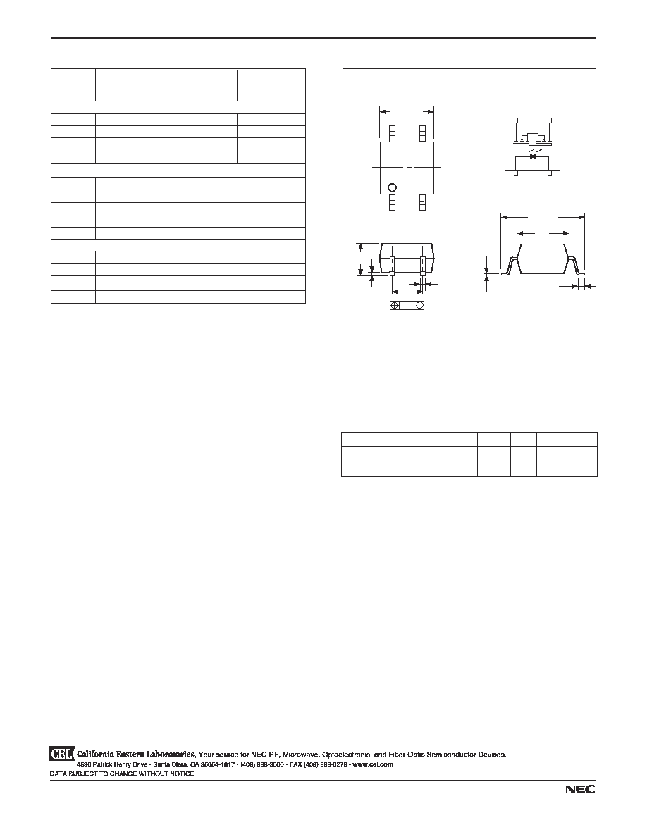
OUTLINE DIMENSIONS
(Units in mm)
1. LED Anode
2. LED Cathode
3. MOS FET
4. MOS FET
RECOMMENDED
OPERATING CONDITIONS
SYMBOL
PARAMETER
UNITS
MIN
TYP
MAX
I
F
LED Operating Current
mA
2
10
20
V
F
LED Off Voltage
V
0
0.5
4.0Ī0.5
2.54
0.5
2.05
0.4
7.0Ī0.3
4.4
0.5Ī0.3
+0.10
-0.05
0.15
1
2
3
4
+0.10
-0.05
0.25
M
+0.08
-0.05
+0.08
-0.05
Life Support Applications
These NEC products are not intended for use in life support devices, appliances, or systems where the malfunction of these products can reasonably be expected
to result in personal injury. The customers of CEL using or selling these products for use in such applications do so at their own risk and agree to fully indemnify
CEL for all damages resulting from such improper use or sale.
A Business Partner of NEC Compound Semiconductor Devices, Ltd.
03/17/2003