 | –≠–ª–µ–∫—Ç—Ä–æ–Ω–Ω—ã–π –∫–æ–º–ø–æ–Ω–µ–Ω—Ç: PS8103 | –°–∫–∞—á–∞—Ç—å:  PDF PDF  ZIP ZIP |

The information in this document is subject to change without notice. Before using this document, please confirm that
this is the latest version.
Not all devices/types available in every country. Please check with local NEC Compound Semiconductor Devices
representative for availability and additional information.
PHOTOCOUPLER
PS8103
HIGH-SPEED (200 kbps) ANALOG OUTPUT TYPE
5-PIN SOP PHOTOCOUPLER
-
Document No. PN10261EJ02V0DS (2nd edition)
Date Published February 2005 CP(K)
Printed in Japan
©
NEC Compound Semiconductor Devices, Ltd. 2003, 2005
-
NEPOC Series
DESCRIPTION
The PS8103 is an optically coupled isolator containing a GaAs LED on the light emitting diode (input side) and a
PIN photodiode and a high-speed amplifier transistor on the output side on one chip.
This is a plastic SOP (Small Out-line Package) type for high density applications.
FEATURES
∑ Wide operating V
CC
range (V
CC
=
-
0.5 to +15 V)
∑ Small package (5-pin SOP)
∑ High isolation voltage (BV = 2 500 Vr.m.s.)
∑ High-speed response (t
PHL
, t
PLH
= 5
µ
s MAX. (@R
L
= 4.1 k
))
∑ Ordering number of taping product: PS8103-F3, F4: 2 500 pcs/reel
∑ Pb-Free
product
∑ Safety
standards
∑ UL approved: File No. E72422
PIN CONNECTION
(Top View)
1. Anode
2. Cathode
3. GND
4. V
O
5. V
CC
5
3
1
2
4
APPLICATIONS
∑ Computer and peripheral manufactures
∑ General purpose inverter
∑ Substitutions for relays and pulse transformers
∑ Power
supply
The mark shows major revised points.
PS8103
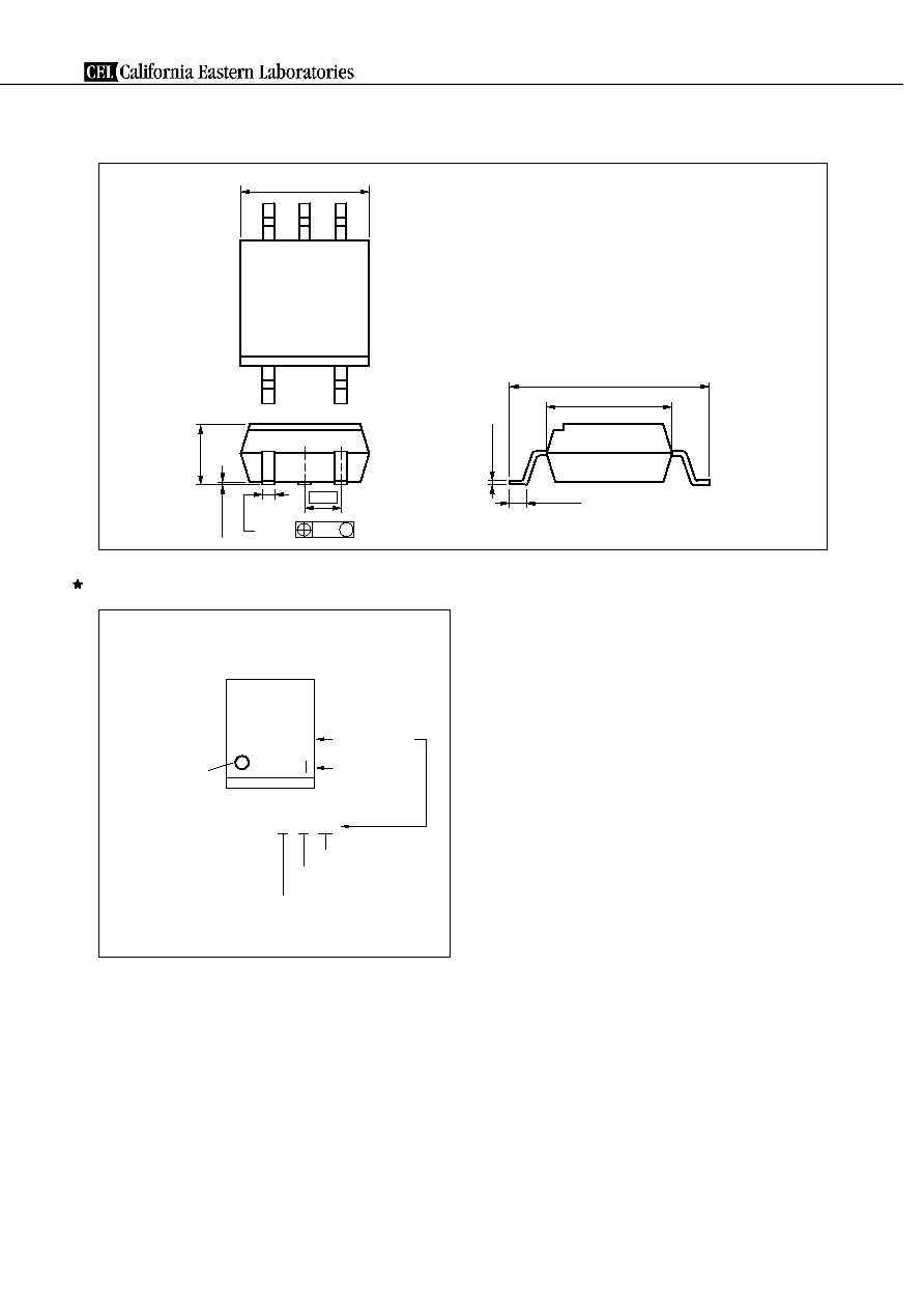
PACKAGE DIMENSIONS (UNIT: mm)
1.27
0.4
+0.10
≠0.05
0.25 M
0.1±0.1
4.4
7.0±0.3
0.5±0.3
0.15
+0.10 ≠0.05
3.4
+0.3
≠0.1
2.6±0.2
MARKING
No. 1 pin Mark
Initial of NEC
(Engraved mark)
Rank Code
Year Assembled
(Last 1 Digit)
Week Assembled
N
2
34
Assembly Lot
8103
N234
N
*1
*1 Bar : Pb-Free
Data Sheet PN10261EJ02V0DS
2

Data Sheet PN10261EJ02V0DS
3
PS8103
ORDERING INFORMATION
Part Number
Order Number
Solder Plating
Specification
Packing Style
Safety Standard
Approval
Application Part
Number
*1
PS8103 PS8103-A
Pb-Free
*2
Magazine case 100 pcs
Standard products
PS8103
PS8103-F3
PS8103-F3-A
Embossed Tape 2 500 pcs/reel (UL approved)
PS8103-F4 PS8103-F4-A
*1 For the application of the Safety Standard, following part number should be used.
*2 With regards to terminal solder (the solder contains lead) plated products (conventionally plated), contact your
nearby sales office.
ABSOLUTE MAXIMUM RATINGS (T
A
= 25
∞
C, unless otherwise specified)
Parameter Symbol
Ratings Unit
Diode Forward
Current
I
F
50 mA
Reverse
Voltage
V
R
5 V
Power Dissipation
*1
P
D
50 mW
Detector Supply Voltage
V
CC
-
0.5 to +15
V
Output
Voltage
V
O
-
0.5 to +15
V
Output
Current
I
O
8 mA
Power
Dissipation
*2
P
C
80 mW
Isolation Voltage
*3
BV 2
500
Vr.m.s.
Operating Ambient Temperature
T
A
-
40 to +100
∞
C
Storage Temperature
T
stg
-
55 to +125
∞
C
*1 Reduced to 0.5 mW/
∞
C at T
A
= 25
∞
C or more.
*2 Applies to output pin V
O
. Reduced to 0.8 mW/
∞
C at T
A
= 25
∞
C or more.
*3 AC voltage for 1 minute at T
A
= 25
∞
C, RH = 60% between input and output.
Pins 1-2 shorted together, 3-4 shorted together.
PS8103
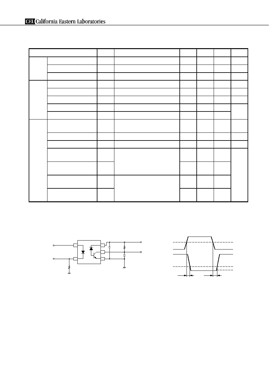
ELECTRICAL CHARACTERISTICS (T
A
= 25∞C)
Parameter Symbol Conditions MIN.
TYP.
MAX.
Unit
Diode Forward
Voltage
V
F
I
F
= 16 mA
1.2
1.5
V
Reverse
Current
I
R
V
R
= 3 V
10
µ
A
Terminal
Capacitance C
t
V = 0 V, f = 1 MHz
30
pF
Detector High Level Output Current
I
OH
(1)
I
F
= 0 mA, V
CC
= V
O
= 5.5 V
7
500
nA
High Level Output Current
I
OH
(2)
I
F
= 0 mA, V
CC
= V
O
= 15 V
100
µ
A
Low Level Output Voltage
V
OL
I
F
= 16 mA, V
CC
= 4.5 V, I
OL
= 1.1 mA
0.1
0.4
V
High Level Supply Current
I
CCH
I
F
= 0 mA, V
O
= open, V
CC
= 15 V
0.01
1
µ
A
Low Level Supply Current
I
CCL
I
F
= 16 mA, V
O
= open, V
CC
= 15 V
150
800
Coupled Current Transfer Ratio (I
C
/I
F
)
*1
CTR I
F
= 16 mA, V
CC
= 4.5 V, V
O
= 0.4 V
10
23
30
%
Isolation
Resistance R
I-O
V
I-O
= 1 kV
DC
, RH = 40 to 60%
10
11
Isolation
Capacitance C
I-O
V = 0 V, f = 1 MHz
0.4
pF
Propagation Delay Time
(H
L)
*2
t
PHL
I
F
= 16 mA, V
CC
= 5 V, R
L
= 4.1 k
,
C
L
= 15 pF
1 5
µ
s
Propagation Delay Time
(L
H)
*2
t
PLH
2
5
Propagation Delay Time
(H
L)
*2
t
PHL
I
F
= 16 mA, V
CC
= 5 V, R
L
= 20 k
,
C
L
= 15 pF
1
15
Propagation Delay Time
(L
H)
*2
t
PLH
7
15
*1 CTR rank
L : 15 to 30 (%)
N : 10 to 30 (%)
*2 Test circuit for propagation delay time
Pulse input (I
F
)
47
(Pulse width = 100 s,
Duty cycle = 1/10)
µ
R
L
= 4.1/20 k
V
O
(Monitor)
V
CC
= 5 V
Input
(Monitor)
0.1 F
µ
C
L
= 15 pF
Input
Output
50%
1.5 V
5 V
V
OL
t
PHL
t
PLH
C
L
includes probe and stray wiring capacitance.
USAGE CAUTIONS
1. This product is weak for static electricity by designed with high-speed integrated circuit so protect against static
electricity when handling.
2. By-pass capacitor of 0.1
µ
F is used between V
CC
and GND near device. Also, ensure that the distance between
the leads of the photocoupler and capacitor is no more than 10 mm.
3. Avoid storage at a high temperature and high humidity.
Data Sheet PN10261EJ02V0DS
4
Data Sheet PN10261EJ02V0DS
5
PS8103
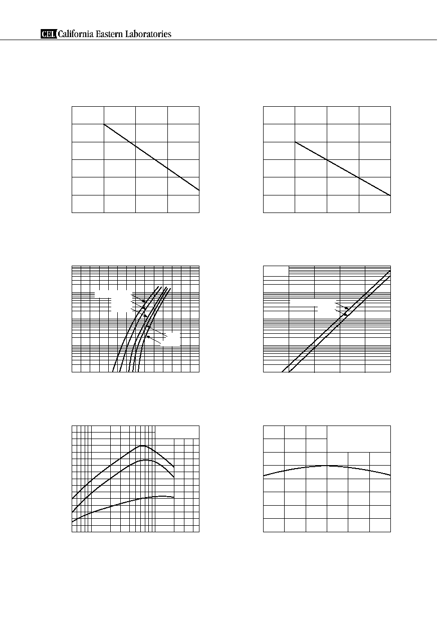
TYPICAL CHARACTERISTICS (T
A
= 25
∞
C, unless otherwise specified)
60
50
30
20
10
0
40
25
50
75
100
Ambient Temperature T
A
(∞C)
Diode Power Dissipation P
D
(mW)
DIODE POWER DISSIPATION vs.
AMBIENT TEMPERATURE
T
A
= +100∞C
+50∞C
+25∞C
0∞C
≠25∞C
100
0.01
0.1
10
1
0.6
1.0
1.2
1.6
0.2
0.4
0.8
1.4
Forward Voltage V
F
(V)
Forward Current I
F
(mA)
FORWARD CURRENT vs.
FORWARD VOLTAGE
V
CC
= 4.5 V,
V
O
= 0.4 V
40
10
0
20
30
35
25
5
15
0.5
5
10
50
1
Forward Current I
F
(mA)
CURRENT TRANSFER RATIO vs.
FORWARD CURRENT
Current Transfer Ratio CTR (
%
)
120
100
60
20
0
80
40
25
50
75
100
Ambient Temperature T
A
(∞C)
Transistor Power Dissipation P
C
(mW)
TRANSISTOR POWER DISSIPATION vs.
AMBIENT TEMPERATURE
I
F
= 0 mA
V
CC
= V
O
= 15 V
5.5 V
1 000
1
0.1
100
10
50
100
≠25
0
25
75
Ambient Temperature T
A
(∞C)
High Level Output Current I
OH
(nA)
HIGH LEVEL OUTPUT CURRENT vs.
AMBIENT TEMPERATURE
1.6
0.0
1.2
0.4
1.4
1.0
0.8
0.6
0.2
0
50
100
≠50
≠25
25
75
Ambient Temperature T
A
(∞C)
Normalized Current Transfer Raio CTR
NORMALIZED CURRENT TRANSFER
RATIO vs. AMBIENT TEMPERATURE
Normalized to 1.0
at T
A
= 25∞C, I
F
= 16 mA,
V
CC
= 4.5 V, V
O
= 0.4 V
Remark The graphs indicate nominal characteristics.