 | ÐлекÑÑоннÑй компоненÑ: UPC3220GR | СкаÑаÑÑ:  PDF PDF  ZIP ZIP |
Äîêóìåíòàöèÿ è îïèñàíèÿ www.docs.chipfind.ru
Notes:
1. By Measurement Circuit 1
2. By Measurement Circuit 4
3. By Measurement Circuit 6
4. By Measurement Circuit 7
DESCRIPTION
The µPC3220GR is silicon monolithic IC designed for use as the
out-of-band tuner for digital CATV applications. This IC consists
of AGC ampliÞ er, low disortion mixer, and video ampliÞ er.
The package is 16-pin SSOP (Shrink Small Outline Package) suit-
able for surface mount.
This IC is manufactured using our 10 GHz fT NESAT II AL silicon
bipolar process.
This process uses silicon nitride passivation Þ lm. This mate-
rial can protect chip surface from external pollution and prevent
corrosion/migration. Thus, this IC has excellent performance,
uniformity and reliability.
NEC's stringent quality assurance and test procedures en sure the
highest reliability and per for mance.
California Eastern Laboratories
ELECTRICAL CHAR AC TER IS TICS
(T
A
= 25°C, V
CC
= 5 V, unless otherwise speciÞ ed)
UPC3220GR
CATV OUT-OF-BAND TUNER
FEATURES
· LOW
DISTORTION:
IIP3 = +1 dBm TYP.
· WIDE AGC DYNAMIC RANGE:
GCRtotal = 46 dB TYP.
· LOW NOISE FIGURE:
7 dB TYP
· HIGH
GAIN:
71 dB TYP
· ON CHIP VIDEO AMPLIFIER
· SINGLE SUPPLY VOLTAGE :
5 V
· PACKAGED IN 16-PIN SSOP SUITABLE FOR HIGH-DENSITY
SURFACE MOUNTING
PART NUMBER
UPC3220GR
SYMBOL
PARAMETERS AND CONDITIONS
UNIT
MIN.
TYP.
MAX.
I
CCTOTAL
Total Circuit Current
1
, No input signal, V
CC1
= V
CC2
= 5 V
mA
33
42
53.5
I
CC1
AGC/Mixer Circuit Current 1
1
, No input signal, V
CC1
= 5 V
mA
15
20
25.5
I
CC2
Video AmpliÞ er Circuit Current 2
1
, No input signal, V
CC2
= 5 V
mA
18.0
22.0
28
V
AGC
(H)
AGC Voltage High Level
1
, at Maximum gain
V
3.0
-
V
CC
V
AGC
(L)
AGC Voltage Low Level
1
, at Minimum gain
V
0
-
0.5
RF Characteristics: AGC Amplifi er Block
(f
RF
= 100 MHz, f
LO
= 136 MHz, P
LO
= -15 dBm, f
IF
= 36 MHz, Z
S
= 50 , Z
L
= 1 k)
f
RF
RF Input Frequency Range
1
MHz
30
-
250
f
IF
IF Output Frequency Range
1
MHz
0.1
-
150
GCR
AGC
AGC Dynamic Range
1
, V
AGC
= 0.5 to 3.0 V
dB
-
46
-
RF Characteristics: Video Amplifi er Block
(f = 36 MHz, Z
S
= 50 , ZL = 1 k)
V
OMAX
2
Maximum Output Voltage
2
, Pin = -25 dBm
Vp-p
2.95
3.90
-
RF Characteristics: Total Block
(f
RF
= 100 MHz, f
LO
= 136 MHz, P
LO
= -15 dBm, f
IF
= 36 MHz, Z
S
= 50 , Z
L
= 1 k)
CG
MAX
Maximum Conversion Gain
3
,
V
AGC
= 3.0 V, Pin = -70 dBm
dB
65.5
71
73.5
CG
MIN
Minimum Conversion Gain
3
, V
AGC
= 0.5 V, Pin = -40 dBm
dB
18
25
31.5
GCR
total
Total Dynamic Range
3
, VAGC = 0.5 to 3.0 V
dB
34
46
-
V
OMAX
Maximum Output Voltage
3
, V
AGC
= 3.0 V, Pin = -45 dBm
Vp-p
2.95
3.90
-
NF
total
Noise Figure
4
, DSB, V
AGC
= 3.0 V (at Maximum gain)
dB
-
7.0
8.5
APPLICATION
· DIGITAL CABLE SETTOP BOXES
· HDTV
RECEIVERS
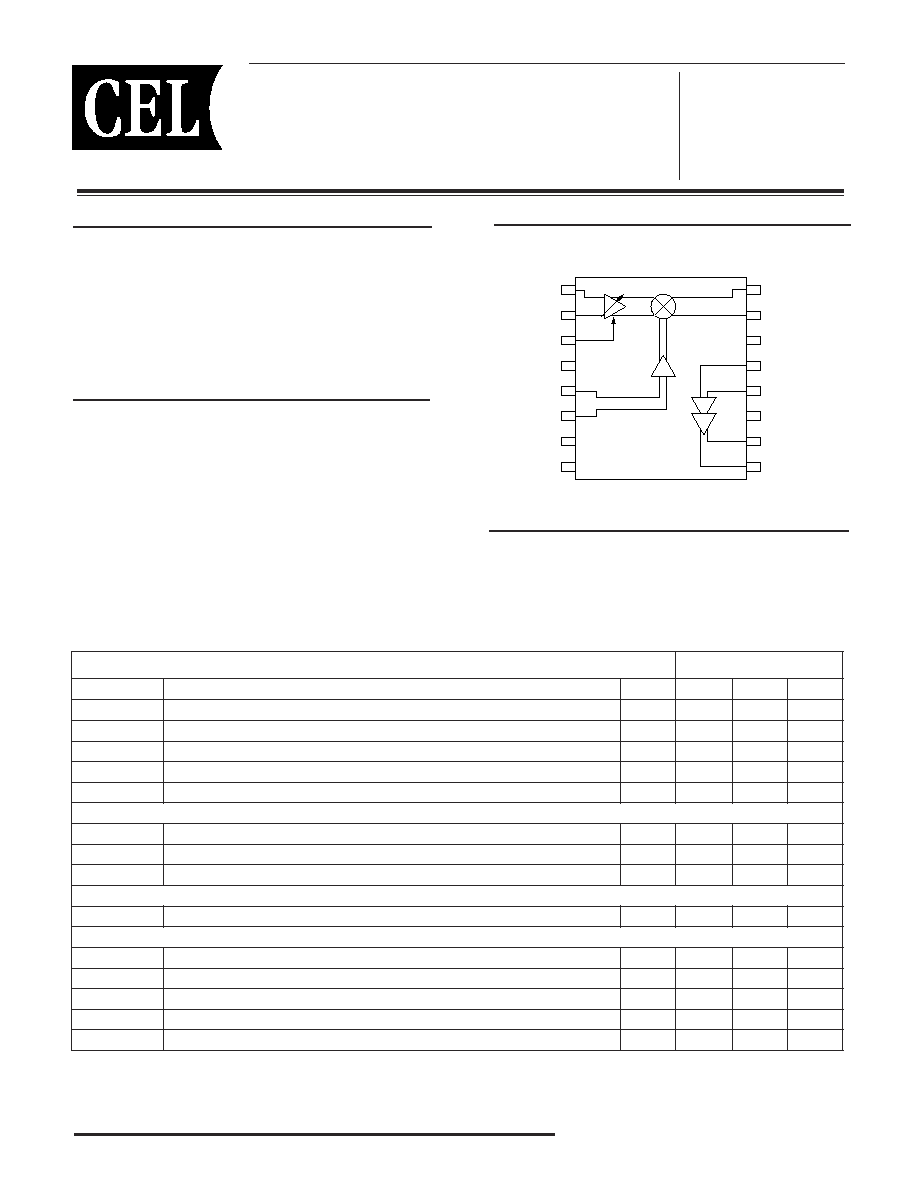
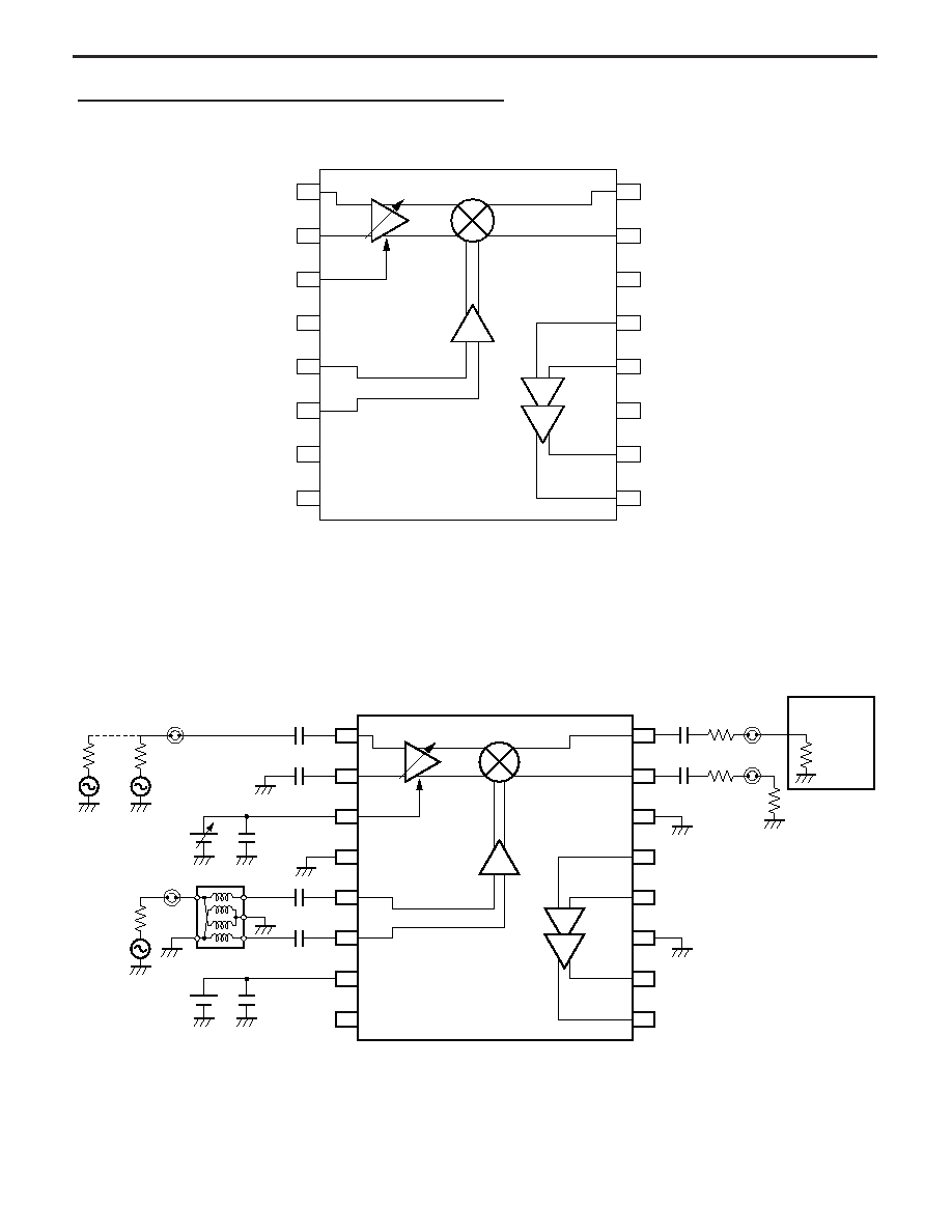
INTERNAL BLOCK DIAGRAM
(Top View)
1
2
3
4
5
6
7
8
16
15
14
13
12
11
10
9
AGC IN1
AGC IN2
V
AGC
GND
OSC IN1
OSC IN2
V
CC
1
V
CC
2
GND
MIX OUT2
MIX OUT1
IN1
IN2
GND
OUT1
OUT2
Video Amp.
AGC Amp.
Mixer
OSC OUT
Buffer Amp.
RECOMMENDED OPERATING CONDITIONS
ABSOLUTE MAXIMUM RATINGS
1
(T
A
= 25°C)
UPC3220GR
STANDARD CHARACTERISTICS
(T
A
= +25°C, V
CC1
= 5 V, Z
S
= 50 )
SYMBOL
PARAMETERS AND CONDITIONS
UNIT
REFERENCE VALUE
AGC Amplifi er+Mixer Block
(f
RF
= 84 MHz, f
LO
= 120 MHz, P
LO
= -15 dBm, f
IF
= 36 MHz, Z
S
= 50 , Z
L
= 1 k)
CG
MAX
Maximum Conversion Gain, V
AGC
= 3.0 V, P
in
= -45 dBm
1
dB
34.0
CG
MIN
Minimum Conversion Gain, V
AGC
= 0.5 V, P
in
= -45 dBm
1
dB
-12.0
NF
Noise Figure, DSB, V
AGC
= 3.0 V (at Maximum gain)
2
dB
7.0
IIP
3
Input 3rd Order Distortion Intercept Point, V
AGC
= 0.5 V (at Minimum gain)
1
dBm
+1.0
V
oclip
Maximum Output Voltage,V
AGC
= 3.0 V, P
in
= -20 dBm
1
V
p-p
0.68
Z
RF
RF Input Impedance, V
AGC
= 3.0 V, f = 84 MHz
3
k
560 j1050
Z
LO
LO Input Impedance, V
AGC
= 3.0 V, f = 120 MHz
3
k
307 - j837
Z
IF
IF Output Impedance, V
AGC
= 3.0 V, f = 36 MHz
3
40.7 + j1.5
Video Amplifi er Block
(f = 36 MHz, Z
S
= 50 , Z
L
= 1 k)
f
BW
Frequency Range, P
in
= -55 dBm, 1 dB down
4
MHz
53
G
diff
Differential Gain, P
in
= -55 dBm
4
dB
51
Z
in
Input Impedance, f = 36 MHz
5
k
620 - j808
Z
out
Output Impedance, f = 36 MHz
5
18 + j12
Total Block
(f
LO
= 120 MHz, P
LO
= -15 dBm, f
IF
= 36 MHz, Z
S
= 50 , Z
L
= 1 k)
IIP
3total
Input 3rd Order Distortion Intercept Point, V
AGC
= 0.5 V (at Minimum gain)
6
dBm
+1.0
IM
3total
3rd Order Intermodulation Distortion, V
out
= 0.7 V
p-p
× 2 tone, P
in
-50 dBm/tone
6
dBc
53
Notes:
1.
By measurement circuit 1
2.
By measurement circuit 2
3.
By measurement circuit 3
4.
By measurement circuit 4
5.
By measurement circuit 5
6.
By measurement circuit 6
SYMBOL
PARAMETERS
UNIT
RATINGS
V
CC
Supply Voltage, T
A
= +25°C
V
6.0
P
D
Power Dissipation, T
A
= +85°C
mW
433
T
A
Operating Ambient Temperature
°C
-40 to +85
T
stg
Storage Temperature
°C
-55 to +150
SYMBOL
PARAMETERS
UNIT
MIN.
TYP.
MAX.
V
CC
Supply Voltage
V
4.5
5.0
5.5
T
A
Operating Ambient Temperature, V
CC
= 4.5 to 5.5 V
°C
-40
+25
+85
V
AGC
Input Power
V
0
-
V
CC
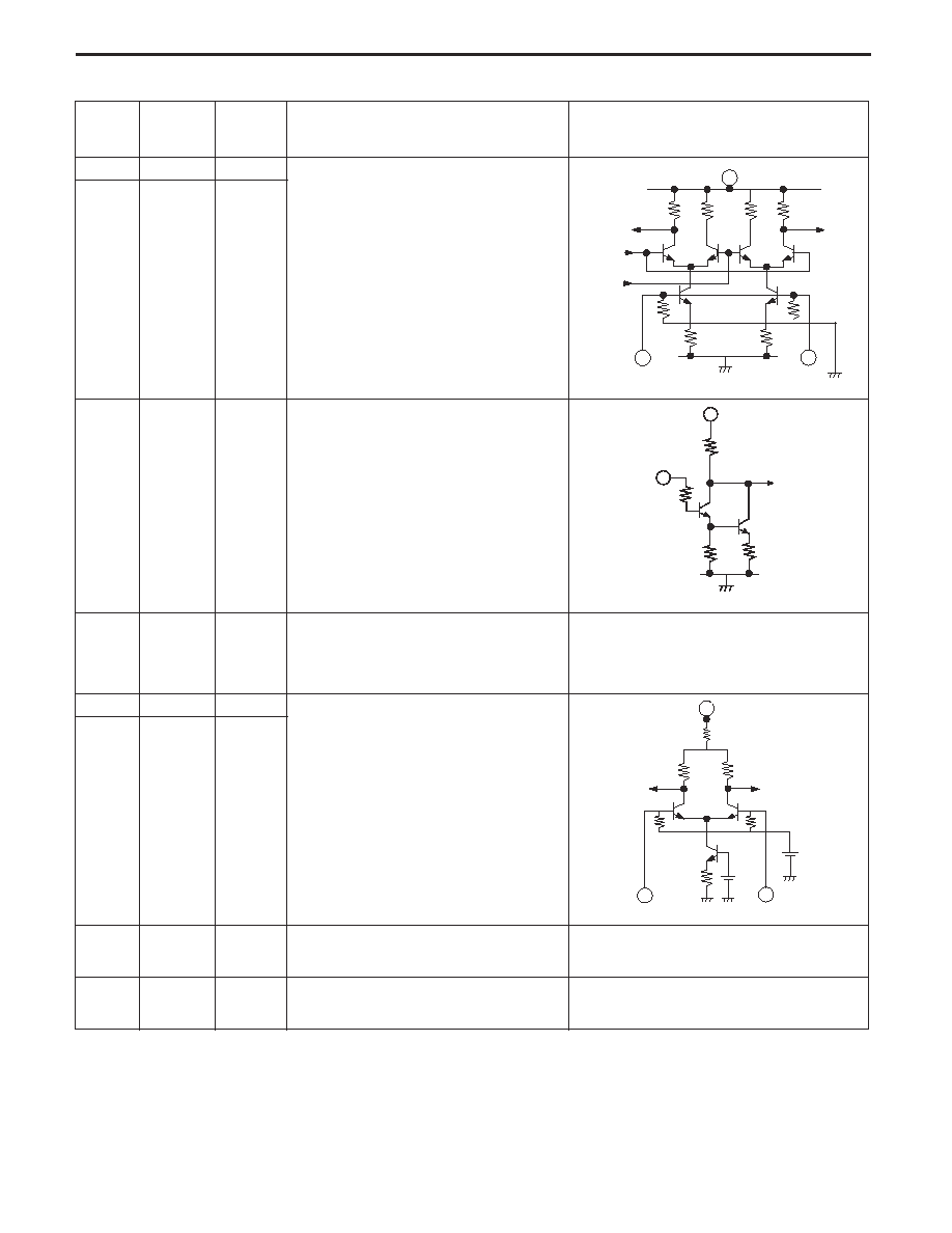
Pin No.
Symbol
Pin Volt-
age
Function and Application
Internal Equivalent Circuit
1
RF IN1
1.46
Input Signal of IF signal.
1 pin is the same phase and 2 pin is opposite
phase at balance input.
In case of single input, 1pin or 2pin should
be grounded through capacitor (ex. 10 nF).
7
1
2
AGC
Control
2
RF IN2
1.46
3
VAGC
0 to 3.5
Automatic gain control pin.
This pn's bias govern the AGC output level.
Minimum gain at VAGC = 0V
Maximum gain at VAGC = 3.5 V
AGC
Control
3
7
4
GND
0.0
Ground pin.
Must be connected to the system ground
with minimum inductance.
Ground pattern on the board should be
formed as wide as possible.
5
OSC IN1
2.6
Input pin of Oscillator signal.
5pin is same phase and 6pin is opposite
phase as balance input.
In case of single input, 5pin or 6 pin should
be grounded through capacitor (ex. 10 nF).
7
5
6
6
OSC IN2
2.6
7
VCC1
5.0
Power supply pin of IF down converter block.
Must be connnected bypass capacitor to
minimize ground impedance.
8
VCC2
5.0
Power supply pin of video ampliÞ er
Must be connnected bypass capacitor to
minimize ground impedance.
PIN FUNCTIONS
UPC3220GR
UPC3220GR
PIN FUNCTIONS
Pin No.
Symbol
Pin Volt-
age
Function and Application
Internal Equivalent Circuit
9
AMP OUT2
2.5
Output pin of video ampliÞ er.
OUT1 and IN1 are same phase.
OUT2 and IN2 are same phase.
8
9
10
10
AMP OUT1
2.5
11
GND
0.0
Ground pin.
Must be connected to the system ground
with minimum inductance.
Ground pattern on the board should be
formed as wide as possible.
12
AMP IN2
1.45
Signal input pin of video ampliÞ er.
This pin is high impedance.
8
13
12
13
AMP IN1
1.45
14
GND
0.0
Ground pin.
Must be connected to the system ground
with minimum inductance.
Ground pattern on the board should be
formed as wide as possible.
15
MIX OUT1
3.7
Output pin of mixer.
This output pin features low-impedance
because of its emitter-follower output port.
7
15
16
16
MIXOUT2
3.7
UPC3220GR
MEASUREMENT CIRCUIT 1
IM3 MEASUREMENT CIRCUIT ON THE AGC/DOWNCONVERTER
INTERNAL BLOCK DIAGRAM AND PIN LAYOUT
(Top View)
1
2
3
4
5
6
7
8
16
15
14
13
12
11
10
9
AGC IN1
AGC IN2
V
AGC
GND
OSC IN1
OSC IN2
V
CC
1
V
CC
2
GND
MIX OUT2
MIX OUT1
IN1
IN2
GND
OUT1
OUT2
Video Amp.
AGC Amp.
Mixer
OSC OUT
Buffer Amp.
1
2
3
4
5
6
7
8
16
15
14
13
12
11
10
9
Video Amp.
AGC Amp.
Mixer
OSC OUT
Buffer Amp.
Note
50
50
RF1
LO
V
AGC
V
CC
1
V
CC
2
RF2
50
1 F
µ
Spectrum
Analyzer
50
50
1 k
1 F
µ
1 k
1 F
µ
1 F
µ
0.1 F
µ
0.1 F
µ
0.1 F
µ
0.1 F
µ
Note: Balun Transformer : TOKO 617DB-1010 B4F (Double balanced type)