Document Outline
- COVER
- DESCRIPTION
- FEATURES
- ORDERING INFORMATION
- BLOCK DIAGRAM
- PIN CONFIGURATION
- PIN DESCRIPTIONS
- LCD DISPLAY
- CHARACTER CODES AND CHARACTER PATTERNS
- DISPLAY RAM ADDRESSES
- PICTOGRAPH DISPLAY RAM ADDRESSES
- CGRAM COLUMN ADDRESSES
- KEY MATRIX AND KEY DATA RAM CONFIGURATION
- KEY REQUEST (KEY REQ)
- LED OUTPUT LATCH CONFIGURATION
- COMMANDS
- STANDBY MODE
- SERIAL COMMUNICATION FORMATS
- ABSOLUTE MAXIMUM RATINGS
- RECOMMENDED OPERATING RANGES
- ELECTRICAL SPECIFICATIONS
- SWITCHING SPECIFICATIONS
- REQUIRED TIMING CONDITIONS
- OUTPUT LOAD CIRCUIT
- SWITCHING SPECIFICATION WAVEFORM DIAGRAMS
- OUTPUT WAVEFORMS
- ACCESS PROCEDURES
- 1. Initialization
- 2. Display Data Rewrite (Address Setting)
- 3. Key Data Read
- 4. CGRAM Write
- 5. Standby (Released by Status Command)
- 6. Standby (Released by KEYN)
- PACKAGE INFORMATION
- REFERENCE DOCUMENTS
MOS INTEGRATED CIRCUIT
Ķ
Ķ
Ķ
Ķ
PD16432B
1998
©
Document No. S11092EJ5V0DS00 (5th edition)
Date Published April 1998 N CP(K)
Printed in Japan
DATA SHEET
1/8, 1/15 DUTY LCD CONTROLLER/DRIVER
DESCRIPTION
The
Ķ
PD16432B is a controller/driver with 1/8 and 1/15 duty dot matrix LCD display capability. It has 60 segment
outputs, 10 common outputs, and 5 dual segment/common outputs, giving a maximum display capability of 12
columns
◊
2 lines (at 1/15 duty).
LED drive outputs, key scanning key source outputs, and key data inputs are also provided, making it ideal for use
in a car stereo front panel, etc.
FEATURES
∑
Dot matrix LCD controller/driver
∑
Pictograph display segment drive capability (max. 64)
∑
LCD driver unit power supply V
LCD
independently settable (Max. 10 V)
∑
On-chip key scan circuit (8
◊
4 matrix)
∑
Alphanumeric character and symbol display capability provided by on-chip ROM (5
◊
7 dots)
240 characters + 16 user-defined characters
∑
Display contents
1/8 duty: 13 columns
◊
1 line, 64 pictograph displays, 4 LEDs
1/15 duty: 12 columns
◊
2 lines, 60 pictograph displays, 4 LEDs
∑
Serial data input/output (SCK, STB, DATA)
∑
On-chip oscillator
∑
Reduced power consumption possible using standby mode
ORDERING INFORMATION
Part Number
Package
Ķ
PD16432BGC-001-9EU
100-pin plastic QFP (0.5 pitch, 14
◊
14), Standard ROM code
2
Ķ
Ķ
Ķ
Ķ
PD16432B
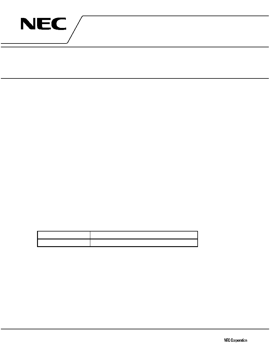
BLOCK DIAGRAM
LED
Driver
LED
1
LED
4
4
4-Bit LED
Output Latch
4
4
STB
SCK
DATA
Serial I/F
RESET
LCD OFF
SYNC
Segment Driver
65-Bit Output Latch
65
65
SEG
1
/KS
1
SEG
8
/KS
8
SEG
9
SEG
60
SEG
61
/COM
14
SEG
65
/COM
10
5
65-Bit Shift Register
Parallel/Serial Conversion
CG
RAM
5
◊
7
◊
16
5
CG ROM
5
◊
7
◊
240
5
8
Display
Data RAM
8
◊
25
8
5
Character
Display
RAM
64 Bits
8
Common Driver
15-Bit Shift Register
15
COM
9
COM
0
5
5
Timing Generator
2
OSC
IN
OSC
OSC
OUT
Key Data
RAM
4
◊
8
KEY
1
KEY
4
Command
Decoder
KEY REQ
V
DD
V
SS
V
LCD
V
LC1
V
LC2
V
LC3
V
LC4
V
LC5
3
Ķ
Ķ
Ķ
Ķ
PD16432B
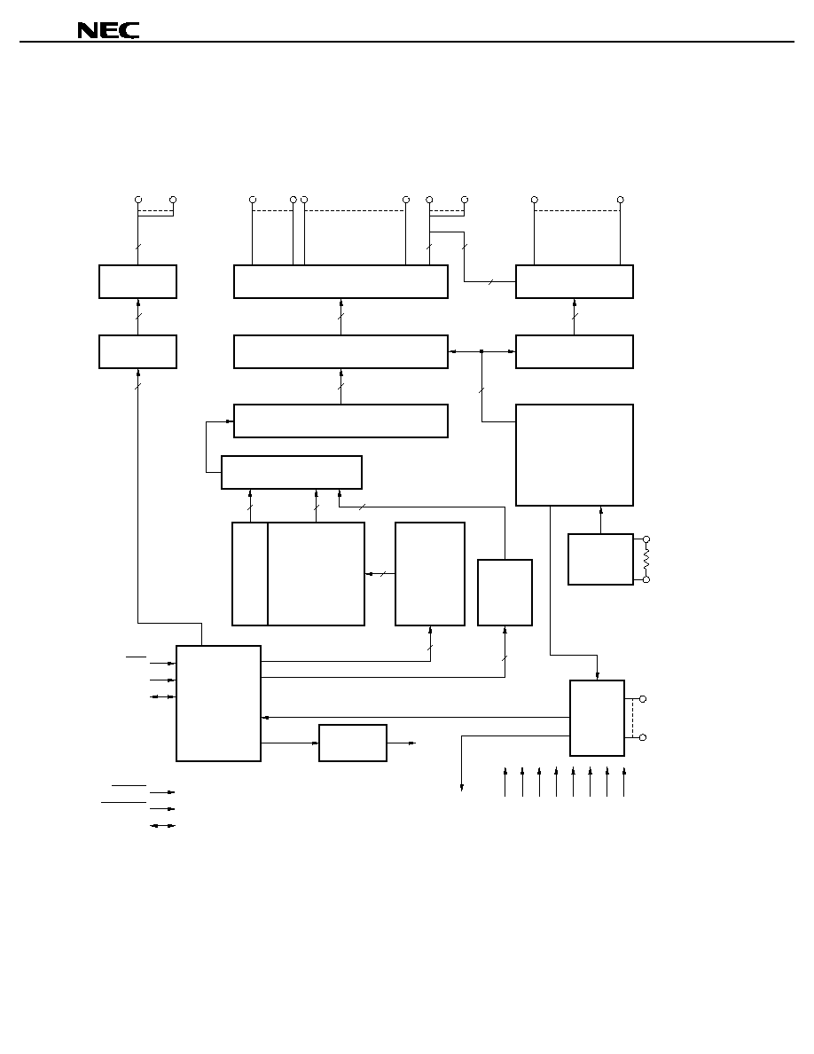
PIN CONFIGURATION
SEG
50
SEG
49
SEG
48
SEG
47
SEG
46
SEG
45
SEG
44
SEG
43
SEG
42
SEG
41
SEG
40
SEG
39
SEG
38
SEG
37
SEG
36
SEG
35
SEG
34
SEG
33
SEG
32
SEG
31
SEG
30
SEG
29
SEG
28
SEG
27
SEG
26
LED
1
LED
2
LED
3
LED
4
V
SS
V
LC5
V
LC4
V
LC3
V
LC2
V
LC1
V
LCD
V
DD
SYNC
LCD OFF
RESET
KEY REQ
SCK
DATA
STB
OSC
IN
OSC
OUT
KEY
1
KEY
2
KEY
3
KEY
4
SEG
25
SEG
24
SEG
23
SEG
22
SEG
21
SEG
20
SEG
19
SEG
18
SEG
17
SEG
16
SEG
15
SEG
14
SEG
13
SEG
12
SEG
11
SEG
10
SEG
9
SEG
8
/KS
8
SEG
7
/KS
7
SEG
6
/KS
6
SEG
5
/KS
5
SEG
4
/KS
4
SEG
3
/KS
3
SEG
2
/KS
2
SEG
1
/KS
1
SEG
51
SEG
52
SEG
53
SEG
54
SEG
55
SEG
56
SEG
57
SEG
58
SEG
59
SEG
60
SEG
61
/COM
14
SEG
62
/COM
13
SEG
63
/COM
12
SEG
64
/COM
11
SEG
65
/COM
10
COM
9
COM
8
COM
7
COM
6
COM
5
COM
4
COM
3
COM
2
COM
1
COM
0
75
51
1
25
26
50
100
76

4
Ķ
Ķ
Ķ
Ķ
PD16432B
PIN DESCRIPTIONS
Pin Symbol
Pin Name
Pin No.
Function
SEG
1
/KS
1
to
SEG
8
/KS
8
Segment output/key source
output dual-function pins
26 to 33
Pins with dual function as dot matrix LCD segment outputs and
key scanning key source outputs
SEG
9
to SEG
60
Segment outputs
34 to 85
Dot matrix LCD segment outputs
SEG
61
/COM
14
to
SEG
85
/COM
10
Segment output/common
output dual-function pins
86 to 90
Switchable to either dot matrix LCD segment outputs or com-
mon outputs
COM
0
to COM
9
Common outputs
91 to 100
Dot matrix LCD common outputs
LED
1
to LED
4
LED output pins
1 to 4
LED outputs are Nch open-drain.
SCK
Shift clock input
17
Data shift clock
Data is read on rising edge, and output on falling edge.
DATA
Data input/output
18
Performs input of commands, key data, etc., and key data
output. Input is performed from the MSB on the rise of the shift
clock, and the first 8 bits are recognized as a command. Output
is performed from the MSB on the fall of the shift clock.
Output is Nch open-drain.
STB
Strobe input
19
Data input is enabled when "H". Command processing is
performed on a fall.
KEY REQ
Key request output
16
"H" if there is key data, "L" if there is none. Key data can be read
irrespective of the state of this pin. Output is CMOS output.
RESET
Reset input
15
Initial state is set when "L".
LCD OFF
LCD off input
14
When "L", a forced LCD off operation is performed, and SEG
n
& COM
n
output the unselected waveform.
SYNC
Synchro
13
Synchronization signal input/output pin. When 2 or more chips
are used, wired-OR connection is made to each chip. A pull-up
resistor is also required when one chip is used.
OSC
IN
20
OSC
OUT
Oscillation pins
21
Connect oscillator resistor.
KEY
1
to KEY
4
Key data inputs
22 to 25
Key scanning key data inputs.
V
DD
Logic power supply pin
12
Internal logic power supply pin
V
SS
GND pin
5
GND pin
V
LCD
LCD drive voltage pin
11
LCD drive power supply pin
V
LC1
to V
LC5
LCD drive power supply
10 to 6
Dot matrix LCD drive power supply
5
Ķ
Ķ
Ķ
Ķ
PD16432B
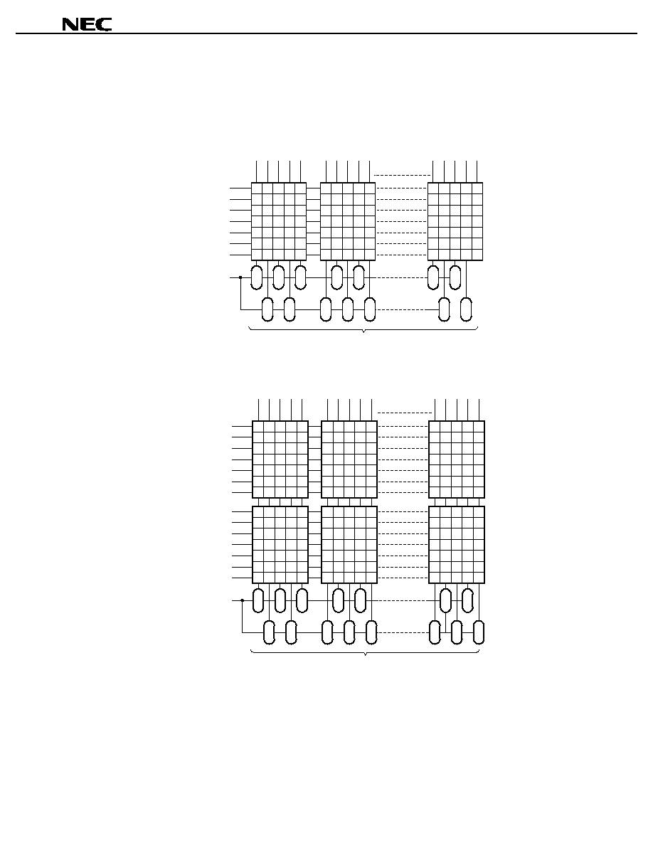
LCD DISPLAY
In the
Ķ
PD16432B LCD display, a 5
◊
7-segment display and pictograph display segments can be driven. The
pictograph display segment common output is allocated to COM
0
, and up to 64 can be driven.
(1) Example of 1/8 duty connections
1
64 Pictograph Segments
SEG
COM1
COM2
COM3
COM4
COM5
COM6
COM7
COM0
2 3 4 5
61 62 63 64 65
6 7 8 9 10
(2) Example of 1/15 duty connections
1
SEG
COM1
COM2
COM3
COM4
COM5
COM6
COM7
2 3 4 5
56 57 58 59 60
6 7 8 9 10
60 Pictograph Segments
COM8
COM9
COM10
COM11
COM12
COM13
COM14
COM0
6
Ķ
Ķ
Ķ
Ķ
PD16432B
CHARACTER CODES AND CHARACTER PATTERNS
The relation between character codes and character patterns is shown below. Character codes 00H to 0FH are
allocated to CGRAM.
Character codes 10H to 1FH and E0H to FFH are undefined.
X0HRAM
Higher
Bits
0XH
CG
(1)
1XH
2XH
3XH
4XH
5XH 6XH
7XH
8XH
9XH AXH BXH CXH DXH EXH FXH
Lower
Bits
X1HRAM
CG
(2)
X2HRAM
CG
(3)
X3HRAM
CG
(4)
X4HRAM
CG
(5)
X5HRAM
CG
(6)
X6HRAM
CG
(7)
X7HRAM
CG
(8)
X8HRAM
CG
(9)
X9HRAM
CG
(10)
XAHRAM
CG
(11)
XBHRAM
CG
(12)
XCHRAM
CG
(13)
XDHRAM
CG
(14)
XEHRAM
CG
(15)
XFHRAM
CG
(16)

7
Ķ
Ķ
Ķ
Ķ
PD16432B
DISPLAY RAM ADDRESSES
Display RAM addresses are allocated as shown below irrespective of the display mode.
Column No.
1
2
3
4
5
6
7
8
9
10
11
12
13
Line 1
00H 01H 02H 03H 04H 05H 06H 07H 08H 09H 0AH 0BH 0CH
Line 2
0DH 0EH 0FH 10H 11H 12H 13H 14H 15H 16H 17H 18H
PICTOGRAPH DISPLAY RAM ADDRESSES
Pictograph display RAM addresses are allocated as shown below.
Segment Output No.
Address
b7
b6
b5
b4
b3
b2
b1
b0
00H
1
2
3
4
5
6
7
8
01H
9
10
11
12
13
14
15
16
02H
17
18
19
20
21
22
23
24
03H
25
26
27
28
29
30
31
32
04H
33
34
35
36
37
38
39
40
05H
41
42
43
44
45
46
47
48
06H
49
50
51
52
53
54
55
56
07H
57
58
59
60
61
62
63
64
Note
When 1/15 duty is used (12 columns
◊
2 lines), 61 to 64 are disabled.

8
Ķ
Ķ
Ķ
Ķ
PD16432B
CGRAM COLUMN ADDRESSES
A maximum of any sixteen 5
◊
7-dot characters can be written in CGRAM. The row address within one character is
allocated as shown below, and is specified by bits b7 to b5.
The character code for which a write is to be performed must be specified beforehand with an address setting
command.
Dot Data
Row
Address
b7
b6
b5
b4
b3
b2
b1
b0
00H
0
0
0
*
*
*
*
*
01H
0
0
1
*
*
*
*
*
02H
0
1
0
*
*
*
*
*
03H
0
1
1
*
*
*
*
*
04H
1
0
0
*
*
*
*
*
05H
1
0
1
*
*
*
*
*
06H
1
1
0
*
*
*
*
*
Row Address
Font Data
(5
◊
7 Dots)
* Font data (1: on, 0: off)
9
Ķ
Ķ
Ķ
Ķ
PD16432B
KEY MATRIX AND KEY DATA RAM CONFIGURATION
The key matrix has an 8
◊
4 configuration, as shown below.
KEY
1
KEY
2
KEY
3
KEY
4
KS
1
KS
2
KS
3
KS
4
KS
5
KS
6
KS
7
KS
8
=
Key data is stored as shown below, and is read in MSB-first order by a read command.
b7
b4 b3
KS
7
Read Order
KS
5
KEY
1
KEY
2
KEY
3
KEY
4
KS
3
KS
1
b0
KS
8
KS
6
KS
4
KS
2
Key data is as follows:
1: On
0: Off
Key Input Equivalent Circuit
KEY
n
V
DD
R
Pull-Up
Control Signal
To Key
Data RAM
In the event of key source output, the pull-up control signal
becomes "H", and the pull-up transistor is turned on.

10
Ķ
Ķ
Ķ
Ķ
PD16432B
KEY REQUEST (KEY REQ)
A key request is output as shown below according to the state.
State
KEY REQ
Note
Key Scan Internal Pull-Up Resistor
In key scan operation
High level is output while any key
data is "1".
Note
During key scan : ON
During display
: OFF
In standby mode or when SEG
n
& COM
n
are fixed at V
LC5
High level is output in case of key
input only.
Always ON
When key scanning is stopped
Fixed at low level
Always OFF
Note
KEY REQ does not become low until the key data is all "0".
(It is not synchronized with the key data reads.)
LED OUTPUT LATCH CONFIGURATION
The low-order 4 bits of the LED output latch are enabled, and the high-order 4 bits disabled, as shown below.
b3
b2
b1
b0
◊
◊
◊
◊
LSB
MSB
◊
: Don't Care
LED
1
LED
2
LED
3
LED
4
Latch data is as follows:
1: On
0: Off

11
Ķ
Ķ
Ķ
Ķ
PD16432B
COMMANDS
Commands set the display mode and status.
The first byte after a rise edge on the STB pin is regarded as a command.
If STB is driven low during command/data transfer, serial communication is initialized and the command/data being
transferred is invalidated. (However, a command or data that has already been transferred is valid.)
(1) Display Setting Command
This command initializes the
Ķ
PD16432B
Note
, and sets the duty, number of segments, number of commons, master/
slave operation, and the drive voltage supply method.
The state set when this command is executed is: LCD off, LED on, key scanning stopped. To restart the display,
it is necessary to execute "status command" normal operation. However, nothing is done if the same mode is
selected.
◊
b2
b1
b0
◊
◊
0
0
LSB
MSB
◊
: Don't Care
Duty setting
0: 1/8 duty (SEG61/COM14 to SEG65/COM10
segment outputs)
1: 1/15 duty (SEG61/COM14 to SEG65/COM10
common outputs)
Master/slave setting
0: Master
1: Slave
Drive voltage supply method selection
0: External
1: Internal
◊
0
0
0
◊
◊
After powering on
Note
When multiple chips are used, only the chip that sent the command is enabled. If initialization is
performed during display, the display may be affected (especially when multiple chips are used).

12
Ķ
Ķ
Ķ
Ķ
PD16432B
(2) Data Setting Command
Sets the data write mode, read mode, and address increment mode.
b3
b2
b1
b0
◊
◊
1
0
LSB
MSB
◊
: Don't Care
Data write mode/read mode setting
000: Write to display data RAM
001: Write to character display RAM
010: Write to CGRAM
011: Write to LED output latch
100: Read key data
Address increment mode setting
(Display data RAM, character display RAM)
0: Increment after data write
1: Address fixed
0
0
0
0
◊
◊
After powering on
(3) Address Setting Command
Sets the display data RAM or character display RAM address.
b3
b2
b1
b0
b4
◊
0
1
LSB
MSB
◊
: Don't Care
Address
Display data RAM
Character display RAM
CGRAM
0
0
0
0
0
◊
After powering on
: 00H to 18H
: 00H to 07H
: 00H to 0FH
Note
If an unspecified address is set, data cannot be written until a correct address is next set. The address
is not incremented even in increment mode.
13
Ķ
Ķ
Ķ
Ķ
PD16432B
(4) Status Command
Controls the status of the
Ķ
PD16432.
b3
b2
b1
b0
b4
b5
1
1
LSB
MSB
LCD cotrol
00: LCD forced off (SEGn, COMn = V
LC5
)
01: LCD forced off (SEGn, COMn = unselected waveform)
10: Normal operation
11: Normal operation
LED control
0: LED forced off
1: Normal operation
Key scan control
0: Key scanning stopped
1: Key scan operation
Test mode setting
0: Normal operation
1: Test mode
Standby mode setting
0: Normal operation
1: Standby mode
Note
0
0
0
0
0
0
After powering on
Note
The following states are use prohibited modes, and key scanning does not operate if these states are
set.
1
0
0
0
0
0
1
1
0
0
0
0
14
Ķ
Ķ
Ķ
Ķ
PD16432B
STANDBY MODE
If standby mode is selected with bit b4 of the status command, the following state is set irrespective of bits b3 to b0
of the status command.
(1) LCD forced off (SEG
n
, COM
n
= V
LC5
)
(2) LED forced off
(3) Key scanning stopped (but KEY
n
= key input wait)
(4) OSC stopped
There are two ways of releasing standby mode, as follows:
(1) Using Status Command
Select normal operation with bit b4 of the status command.
Example of Use of Status Command
Command/Data
Item
STB
b7
b6
b5
b4
b3
b2
b1
b0
Description
Standby mode
L
Status command
H
1
1
0
0
0
0
0
0
Standby release (OSC oscillation start), LCD
control off (SEG
n
, COM
n
= V
LC5
), LED forced
off, key scanning stopped
Standby transition time
L
10
Ķ
s
Note
Status command
H
1
1
0
0
1
1
1
0
Normal operation
End
L
Note
If LCD normal operation or key scan operation is initiated within the standby transition time, the LCD
may flicker.

15
Ķ
Ķ
Ķ
Ķ
PD16432B
(2) Using KEY
n
If any key is set to the ON state, the standby mode is released and OSC oscillation starts. Also, KEY REQ is set
to "H", informing the microcomputer that a key has been pressed and standby mode has been released. In this
state, the key data is not memorized, and therefore it is necessary to set key scanning to the normal state after
the standby transition time, and fetch the key data.
Example of Use of KEY
n
Command/Data
Item
STB
b7
b6
b5
b4
b3
b2
b1
b0
Description
Standby mode
L
Key data present
L
Standby release (KEY REQ = H,
OSC oscillation start)
Standby transition time
L
10
Ķ
s
Note
Status command
H
1
1
0
0
1
0
0
1
LCD forced off (unselected waveform),
LED forced off, key scan operation
Key scan
L
1 frame or more
Data setting command
H
0
1
0
0
0
1
0
0
Key data read, address increment
Key data
H
*
*
*
*
*
*
*
*
For KS
8
, KS
7
Key data
H
*
*
*
*
*
*
*
*
For KS
6
, KS
5
Key data
H
*
*
*
*
*
*
*
*
For KS
4
, KS
3
Key data
H
*
*
*
*
*
*
*
*
For KS
2
, KS
1
End
L
Key distinction
Note
If LCD normal operation or key scan operation is initiated within the standby transition time, the LCD
may flicker.
16
Ķ
Ķ
Ķ
Ķ
PD16432B
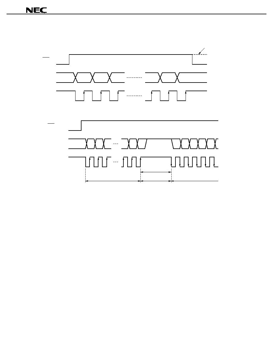
SERIAL COMMUNICATION FORMATS
(1) Reception (Command/Data Write)
SCK
1
2
3
6
7
8
DATA
b7
STB
b6
b5
b1
b0
b2
If data continues
(2) Transmission (Command/Data Read)
SCK
DATA
STB
1
2
3
6
7
8
1
2
3
4
5
6
b7
b6
b5
b2
b1
b0
b7
b6
b5
b4
b3
1 s
Ķ
Wait Time t
WAIT
Data Read
Data Read Command Setting
Caution
As the DATA pin is an Nch open-drain output, a pull-up resistor must be connected
externally. (1 k
to 10 k
)

17
Ķ
Ķ
Ķ
Ķ
PD16432B
ABSOLUTE MAXIMUM RATINGS (T
A
= 25įC, V
SS
= 0 V)
Parameter
Symbol
Rating
Unit
Logic supply voltage
V
DD
≠0.3 to +7.0
V
Logic input voltage
V
IN
≠0.3 to +V
DD
+ 0.3
V
Logic output voltage (Dout, LED)
V
OUT
≠0.3 to +7.0
V
LCD drive supply voltage
V
LCD
≠0.3 to +12.0
V
LCD drive power supply input voltage
V
LC1
to V
LC5
≠0.3 to +V
LCD
+ 0.3
V
Driver output voltage
(Segment, Common)
V
OUT2
≠0.3 to +V
LCD
+ 0.3
V
LED drive current
I
OL1
20
mA
Package allowable dissipation
P
T
1000
mW
Operating ambient temperature
T
A
≠40 to +85
įC
Storage temperature range
T
stg
≠55 to +150
įC
RECOMMENDED OPERATING RANGES
Parameter
Symbol
MIN.
TYP.
MAX.
Unit
Logic supply voltage
V
DD
2.7
5.0
5.5
V
LCD drive supply voltage
V
LCD
V
DD
8.0
10.0
V
Logic input voltage
V
IN
0
V
DD
V
Driver input voltage
V
LCD1
to V
LCD5
0
V
LCD
V
LED drive current
I
OL1
15
mA

18
Ķ
Ķ
Ķ
Ķ
PD16432B
ELECTRICAL SPECIFICATIONS
(UNLESS SPECIFIED OTHERWISE, T
A
= ≠40 to +85įC, V
DD
= 5 V
Ī
Ī
Ī
Ī
10%, V
LCD
= 8 V
Ī
Ī
Ī
Ī
10%)
Parameter
Symbol
Test Conditions
MIN.
TYP.
MAX.
Unit
High-level input voltage
V
IH
0.7 V
DD
V
DD
V
Low-level input voltage
V
IL
0
0.3 V
DD
V
High-level input current
I
IH
SCK, STB, LCDOFF, RESET, KEY
1
to KEY
4
1
Ķ
A
Low-level input current
I
IL
SCK, STB, LCDOFF, RESET, KEY
1
to KEY
4
≠1
Ķ
A
Low-level output voltage
V
OL1
LED
1
to LED
4
, I
OL1
= 15 mA
1.0
V
High-level output voltage
V
OH2
OSC
OUT
, KEY REQ, I
OH2
= ≠1 mA
0.9 V
DD
V
Low-level output voltage
V
OL2
DATA, OSC
OUT
, SYNC, I
OL2
= 4 mA
0.1 V
DD
V
High-level leak current
I
LOH2
DATA, SYNC, V
IN/OUT
= V
DD
1
Ķ
A
Low-level leak current
I
LOL2
DATA, SYNC, V
IN/OUT
= V
SS
≠1
Ķ
A
Common output ON-
resistance
R
COM
V
LCD
to V
LC5
COM
0
to COM
14
, | I
O
| = 100
Ķ
A
2.4
k
Segment output ON-
resistance
R
SEG
V
LCD
to V
LC5
SEG
1
to SEG
60
, | I
O
| = 100
Ķ
A
4.0
k
I
DD1
Normal operation
Note
, V
I
= V
DD
or V
SS
,
f
OSC
= 250 kHz
500
Ķ
A
Current consumption
(Logic)
I
DD2
Standby mode, V
I
= V
DD
or V
SS
, f
OSC
stopped
5
Ķ
A
I
LCD1
Normal operation, internal bias selected, no load
1 000
Ķ
A
Current consumption
(Driver)
I
LCD2
Standby mode, internal bias used, no load
5
Ķ
A
Note
Normal operation: V
DD
= 5 V, V
LCD
= 8 V
Remarks TYP. values are reference values for T
A
= 25įC.

19
Ķ
Ķ
Ķ
Ķ
PD16432B
SWITCHING SPECIFICATIONS
(UNLESS SPECIFIED OTHERWISE, T
A
= ≠40 to +85įC, V
DD
= V
LCD
= 5 V
Ī
Ī
Ī
Ī
10%, R
L
= 5 k
, C
L
= 150 pF)
Parameter
Symbol
Test Conditions
MIN.
TYP.
MAX.
Unit
Oscillator frequency
f
OSC
R = 100 k
175
250
325
kHz
Output data delay time
t
PZL
SCK
DATA
100
ns
Output data delay time
t
PLZ
SCK
DATA
300
ns
SYNC delay time
t
DSYNC
1.5
Ķ
s
Note
The time for one frame is found as follows.
1 frame = 1/f
OSC
◊
128 clocks
◊
duty number + 1/f
OSC
◊
64 clocks
If f
OSC
= 250 kHz and duty = 1/15, 1 frame = 4
Ķ
s
◊
128
◊
15 + 4
Ķ
s
◊
64 = 7.94 ms
REQUIRED TIMING CONDITIONS
(UNLESS SPECIFIED OTHERWISE, T
A
= ≠40 to +85įC, V
DD
= 5 V
Ī
Ī
Ī
Ī
10%, V
LCD
= 8 V
Ī
Ī
Ī
Ī
10%, R
L
= 5 k
,
C
L
= 150 pF)
Parameter
Symbol
Test Conditions
MIN.
TYP.
MAX.
Unit
Clock frequency
f
OSC
OSC
IN
external clock
100
500
kHz
High-level clock pulse width
t
WHC
OSC
IN
external clock
1
5
Ķ
s
Low-level clock pulse width
t
WLC
OSC
IN
external clock
1
5
Ķ
s
Shift-clock cycle
t
CYK
SCK
900
ns
High-level shift clock pulse width
t
WHK
SCK
400
ns
Low-level shift clock pulse width
t
WLK
SCK
400
ns
Shift clock hold time
t
HSTBK
STB
SCK
1.5
Ķ
s
Data setup time
t
DS
DATA
SCK
100
ns
Data hold time
t
DH
SCK
DATA
200
ns
STB hold time
t
HKSTB
SCK
STB
1
Ķ
s
STB hold time
t
WSTB
1
Ķ
s
Wait time
t
WAIT
8th SCK
9th SCK
, in data read
1
Ķ
s
SYNC removal time
t
SREM
250
ns
Standby transition time
t
PSTB
10
Ķ
s
Reset pulse width
t
WRS
RESET
0.1
Ķ
s
Power-ON reset time
t
PON
From Power-ON
4
CLK

20
Ķ
Ķ
Ķ
Ķ
PD16432B
OUTPUT LOAD CIRCUIT
V
DD
5 k
150 pF
DATA
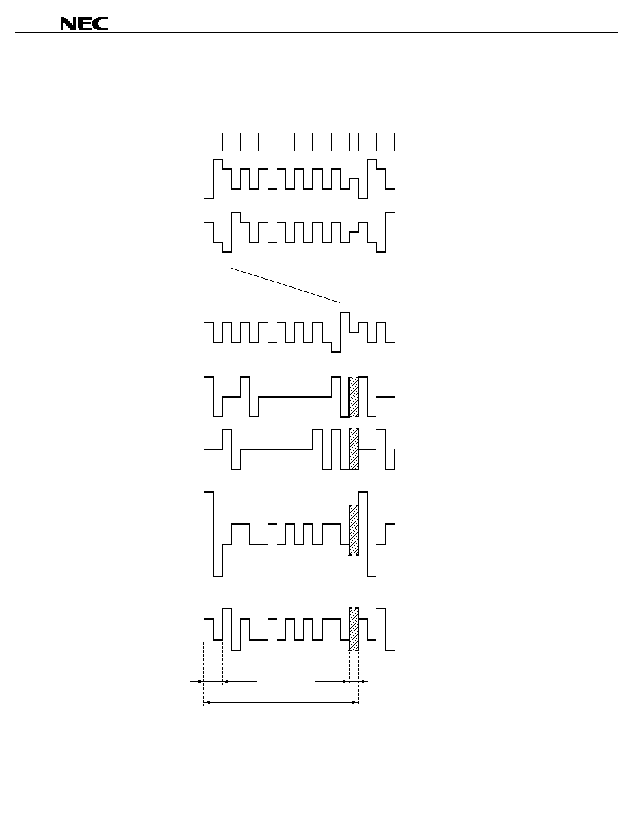
SWITCHING SPECIFICATION WAVEFORM DIAGRAMS
OSC
IN
V
IL
V
IH
1/f
C
t
WHC
t
WLC
V
IH
V
IH
V
IL
t
HSTBK
t
WSTB
t
CYK
t
WLK
t
WLK
V
IL
V
IH
V
IL
V
IH
t
DS
t
DH
t
HKSTB
STB
SCK
DATA

21
Ķ
Ķ
Ķ
Ķ
PD16432B
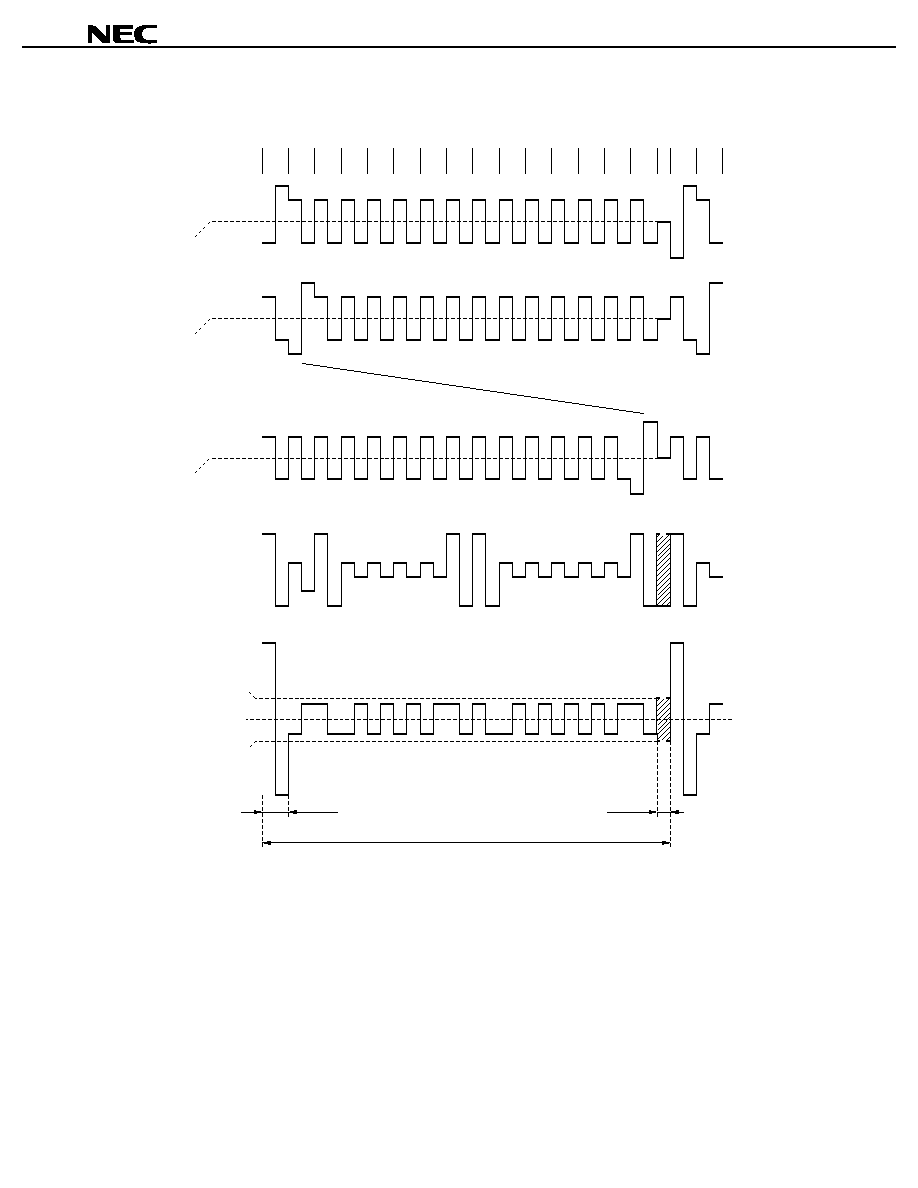
SWITCHING SPECIFICATION WAVEFORM DIAGRAMS
f
OSC
SYNC
Internal Reset
One Frame
One Frame
SYNC Timing (Master)
t
DSYNC
One Frame
One Frame
SYNC Timing (Slave)
t
SREM
t
PZL
V
IL
V
OL2
t
PLZ
SCK
DATA
RESET
RESET
t
WRE
22
Ķ
Ķ
Ķ
Ķ
PD16432B
OUTPUT WAVEFORMS
(1) 1/8 Duty (1/4 Bias: VLC2: VLC3)
V
LCD
V
LC1
V
LC2
V
LC4
V
LC5
COM
0
0
1
2
3
4
5
6
7
K
0
1
*
V
LCD
V
LC1
V
LC2
V
LC4
V
LC5
COM
1
V
LCD
V
LC1
V
LC2
V
LC4
V
LC5
COM
7
V
LCD
V
LC1
V
LC2
V
LC4
V
LC5
SEG
2
V
LCD
V
LC1
V
LC2
V
LC4
V
LC5
SEG
1
V
LCD
3/4V
LCD
2/4V
LCD
≠1/4V
LCD
≠2/4V
LCD
SEG
1
-COM
1
≠3/4V
LCD
1/4V
LCD
0
≠V
LCD
V
LCD
3/4V
LCD
2/4V
LCD
≠1/4V
LCD
≠2/4V
LCD
SEG
1
-COM
0
≠3/4V
LCD
1/4V
LCD
0
≠V
LCD
256 s
512 s
Ķ
Ķ
4.4 ms
* Key scan period

23
Ķ
Ķ
Ķ
Ķ
PD16432B
Enlargement of Key Scan Period
7
1
2
3
4
5
6
7
8
0
V
LCD
V
LC1
V
LC2
V
LC4
V
LC5
SEG
1
K
SEG
1
V
LCD
V
LC1
V
LC2
V
LC4
V
LC5
COM
0
V
LCD
V
LC1
V
LC2
V
LC4
V
LC5
SEG
2
V
LCD
V
LC1
V
LC2
V
LC4
V
LC5
SEG
8
V
LCD
V
LC1
V
LC2
V
LC4
V
LC5
SEG
9
to SEG
65
= Key source output
24
Ķ
Ķ
Ķ
Ķ
PD16432B
(2) 1/15 Duty (1/5 Bias)
256 s
V
LCD
V
LC1
V
LC2
V
LC3
V
LC4
COM
0
1/2V
LCD
V
LC5
0
1
2
3
4
5
6
7
8
9
10
11
12
13
14 K
1
2
*
* Key scan period
V
LCD
V
LC1
V
LC2
V
LC3
V
LC4
COM
1
1/2V
LCD
V
LC5
V
LCD
V
LC1
V
LC2
V
LC3
V
LC4
COM
14
1/2V
LCD
V
LC5
V
LCD
V
LC1
V
LC2
V
LC3
V
LC4
SEG
1
V
LC5
V
LCD
3/5V
LCD
1/2V
LCD
≠1/5V
LCD
≠1/2V
LCD
SEG
1
-COM
0
≠3/5V
LCD
1/5V
LCD
0
≠V
LCD
512 s
Ķ
Ķ
7.9 ms
25
Ķ
Ķ
Ķ
Ķ
PD16432B
Enlargement of Key Scan Period
SEG
9
to SEG
65
SEG
8
SEG
2
14
1
2
3
4
5
6
7
8
0
V
LC5
V
LC1
V
LC2
V
LC3
V
LC4
SEG
1
K
V
LCD
V
LC1
V
LC2
V
LC3
V
LC4
COM
0
V
LC5
V
LC1
V
LC2
V
LC3
V
LC4
V
LCD
V
LC1
V
LC2
V
LC4
V
LC5
V
LC1
V
LC2
V
LC3
V
LC4
V
LC5
= Key source output
V
LCD
V
LC5
V
LCD
1/2V
LCD
V
LCD
V
LC3

26
Ķ
Ķ
Ķ
Ķ
PD16432B
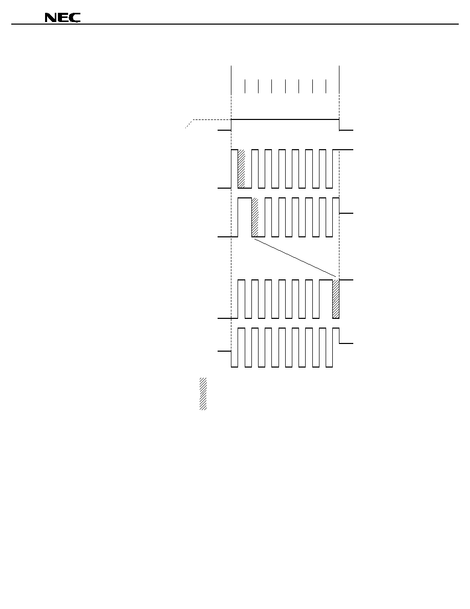
ACCESS PROCEDURES
Access procedures are illustrated below by means of flowcharts and timing charts.
1.
Initialization
(1) Flowchart
0
1
0
1
0
0
0
0
LSB
MSB
Display setting command (command 1)
(1/15 duty, master, internal drive)
Initial state
initialization
1
0
0
1
0
0
1
1
LSB
MSB
Status command (command 2)
(LCD off, LED off, key scan operation)
Key scan start
0
0
0
0
0
0
1
0
LSB
MSB
Data setting command (command 3)
(Display data RAM, increment)
Display data RAM
write
0
0
0
0
0
0
0
1
LSB
MSB
Address setting command (command 4)
(Display data RAM: 0H)
Address setting
Start
Display data
0
0
0
1
0
0
1
0
LSB
MSB
Data setting command (command 5)
(Character display RAM, increment)
Character display
RAM write
Character data
All data written?
All data written?
NO
NO
YES
YES

27
Ķ
Ķ
Ķ
Ķ
PD16432B
0
0
1
1
0
0
1
0
LSB
MSB
Data setting command (command 6)
(LED latch, increment)
LED output latch
write
LED data
1
1
1
0
0
0
1
1
LSB
MSB
Status command (command 7)
(LCD on, LED on, key scan operation)
To next processing
LCD, LED on
(2) Timing chart
DATA
SCK
STB
Command 1
Command 2
Command 3
Command 4
Data 1
DATA
SCK
STB
Data n-1
Data n
Command 5
Data 1
DATA
SCK
STB
Data n
Command 6
Data
Command 7

28
Ķ
Ķ
Ķ
Ķ
PD16432B
2.
Display Data Rewrite (Address Setting)
(1) Flowchart
1
0
0
0
0
0
1
0
LSB
MSB
Data setting command (command 1)
(Display data RAM, address fixed)
Display data RAM
write
0
1
0
1
0
0
0
1
LSB
MSB
Address setting command (command 2)
(Display data RAM: 5H)
Address setting
To next processing
Display data
Start
(2) Timing chart
DATA
SCK
Command 1
Command 2
Data
STB
29
Ķ
Ķ
Ķ
Ķ
PD16432B
3.
Key Data Read
(1) Flowchart
KEY REQ
recognition
Start
0
1
0
0
0
0
1
0
LSB
MSB
Data setting command (command 1)
(Key data)
KEY REQ = H?
NO
YES
Key data read
Wait OK?
NO
YES
All data read?
NO
YES
To next processing
Key data
Wait time: 1 s
Ķ
(2) Timing chart
DATA
SCK
STB
Command 1
Data 1
Data 2
Data 3
KEY REQ
DATA
SCK
STB
Data 4
KEY REQ
t
WAIT
Cautions 1. Wait time t
WAIT
(1
Ķ
Ķ
Ķ
Ķ
s) is necessary from the rise of the 8th shift clock of command 1
until the fall of the 1st shift clock of data 1.
2. KEY REQ does not become low until the key data is all "0".
(It is not synchronized with the key data reads.)

30
Ķ
Ķ
Ķ
Ķ
PD16432B
4.
CGRAM Write
(1) Flowchart
0
0
1
0
0
0
1
0
LSB
MSB
Data setting command (command 1)
(CGRAM, increment)
0
0
0
0
0
0
0
1
LSB
MSB
Address setting command (command 2)
(CGRAM character code: 0H)
Address setting
CGRAM data
Start
To next processing
All data written?
NO
YES
CGRAM write
(2) Timing chart
DATA
SCK
STB
Command 1
Command 2
Data 1
Data 2
DATA
SCK
STB
Data 6
Data 7

31
Ķ
Ķ
Ķ
Ķ
PD16432B
5.
Standby (Released by Status Command)
(1) Flowchart
0
0
0
0
1
0
1
1
LSB
MSB
Status command (command 1)
(Standby)
0
0
0
0
0
0
1
1
LSB
MSB
Status command (command 2)
(Standby release)
Standby release
To next processing
Normal operation
Start
1
1
1
0
0
0
1
1
LSB
MSB
Status command (command 3)
(LCD on, LED on, key scan operation)
Transition
time OK?
NO
Standby transition time: 10 s
Standby
Ķ
YES
(2) Timing chart
DATA
SCK
STB
Command 1
Command 2
Command 3
t
STBY
32
Ķ
Ķ
Ķ
Ķ
PD16432B
6.
Standby (Released by KEY
N
)
(1) Flowchart
Key (KEY
n
) input
KEY REQ = H, OSC oscillation start
0
0
0
0
1
0
1
1
LSB
MSB
Status command (command 1)
(Standby)
Key request
To next processing
Normal operation
Start
1
1
1
0
0
0
1
1
LSB
MSB
Status command (command 2)
(LCD on, LED on, key scan operation)
Transition
time OK?
NO
Standby transition time: 10 s
Standby
Ķ
YES
(2) Timing chart
DATA
SCK
STB
Command 1
Command 2
t
STBY
KEY REQ
33
Ķ
Ķ
Ķ
Ķ
PD16432B
PACKAGE INFORMATION (UNIT: mm)
100 PIN PLASTIC TQFP (FINE PITCH) ( 14)
ITEM
MILLIMETERS
INCHES
A
NOTE
Each lead centerline is located within 0.10 mm (0.004 inch) of
its true position (T.P.) at maximum material condition.
S
A
16.0Ī0.2
0.630Ī0.008
B
14.0Ī0.2
0.551+0.009
≠0.008
C
14.0Ī0.2
0.551+0.009
≠0.008
S100GC-50-9EU-1
S
1.27 MAX.
0.050 MAX.
K
1.0Ī0.2
0.039+0.009
≠0.008
L
0.5Ī0.2
0.020+0.008
≠0.009
M
0.145
0.006Ī0.002
N
0.10
0.004
P
1.0Ī0.1
0.039+0.005
≠0.004
Q
0.1Ī0.05
0.004Ī0.002
+0.055
≠0.045
B
C
D
J
H
I
G
F
P
N
L
K
M
Q
R
R
3į
3į
+7į
≠3į
+7į
≠3į
detail of lead end
M
75
76
50
26
25
51
100
1
D
F
1.0
16.0Ī0.2
0.630Ī0.008
0.039
G
1.0
0.039
H
0.22
0.009Ī0.002
I
J
0.5 (T.P.)
0.10
0.004
0.020 (T.P.)
+0.05
≠0.04

34
Ķ
Ķ
Ķ
Ķ
PD16432B
REFERENCE DOCUMENTS
NEC Semiconductor Device Reliability/Quality Control System
(IEI-1212)
Semiconductor Device Mounting Technology Manual
(C10535E)

35
Ķ
Ķ
Ķ
Ķ
PD16432B
[MEMO]

Ķ
Ķ
Ķ
Ķ
PD16432B
No part of this document may be copied or reproduced in any form or by any means without the prior written
consent of NEC Corporation. NEC Corporation assumes no responsibility for any errors which may appear in this
document.
NEC Corporation does not assume any liability for infringement of patents, copyrights or other intellectual
property rights of third parties by or arising from use of a device described herein or any other liability arising
from use of such device. No license, either express, implied or otherwise, is granted under any patents,
copyrights or other intellectual property rights of NEC Corporation or others.
While NEC Corporation has been making continuous effort to enhance the reliability of its semiconductor devices,
the possibility of defects cannot be eliminated entirely. To minimize risks of damage or injury to persons or
property arising from a defect in an NEC semiconductor device, customers must incorporate sufficient safety
measures in its design, such as redundancy, fire-containment, and anti-failure features.
NEC devices are classified into the following three quality grades:
"Standard", "Special", and "Specific". The Specific quality grade applies only to devices developed based on
a customer designated "quality assurance program" for a specific application. The recommended applications
of a device depend on its quality grade, as indicated below. Customers must check the quality grade of each
device before using it in a particular application.
Standard: Computers, office equipment, communications equipment, test and measurement equipment,
audio and visual equipment, home electronic appliances, machine tools, personal electronic
equipment and industrial robots
Special: Transportation equipment (automobiles, trains, ships, etc.), traffic control systems, anti-disaster
systems, anti-crime systems, safety equipment and medical equipment (not specifically designed
for life support)
Specific: Aircrafts, aerospace equipment, submersible repeaters, nuclear reactor control systems, life
support systems or medical equipment for life support, etc.
The quality grade of NEC devices is "Standard" unless otherwise specified in NEC's Data Sheets or Data Books.
If customers intend to use NEC devices for applications other than those specified for Standard quality grade,
they should contact an NEC sales representative in advance.
Anti-radioactive design is not implemented in this product.
M4 96. 5