Document Outline
- 1.0 Introduction
- 2.0 Signal Summary
- 3.0 Register, Resource, and Implementation
- 4.0 CPU Interface
- 5.0 Memory Interface
- 6.0 PCI Bus Interface
- 7.0 DMA Transfers
- 8.0 Interrupts
- 9.0 Clocking
- 10.0 Reset Configuration Signals
- 11.0 Endian Mode Software Issues
- 12.0 Timing Diagrams
- 13.0 Testing
- 14.0 Electrical Specifications
- 15.0 Pinout
- 16.0 Package

Data Sheet
U13023EU1V0DSU1
1.0
Introduction
1.1
Overview
The V
RC
4373
TM
system controller is a software-configurable chip that directly interfaces
the V
R
4300
TM
CPU and PCI bus without external logic or buffering, and also interfaces
memory (SDRAM, EDO, fast-page DRAM, and flash boot ROM) with minimal buffer-
ing. From the viewpoint of the V
R
4300 CPU, the V
RC
4373 acts as a memory controller,
DMA controller, and PCI bridge. From the viewpoint of PCI agents, the V
RC
4373 acts
as either a PCI bus master or a PCI bus target. Alternatively, the V
RC
4373 may be
located on a PCI bus add-on board.
1.2
Features
q
CPU Interface
�
Direct connection to the 66MHz V
R
4300 CPU bus
�
3.3V I/O
�
Support for all V
R
4300 bus cycles
�
Little-endian or big-endian byte order
q
Memory Interface
�
Support for boot ROM, base memory, and up to four SIMM
TM
(DIMM) ranges
�
Programmable address ranges for base memory and SIMM memory
�
66 MHz memory bus
�
Base memory range: SDRAM and EDO DRAM
�
SIMM memory range: SDRAM, EDO and fast-page DRAM, and flash ROM
�
Several speed grades supported within each memory range
�
Bank-interleaved or non-bank-interleaved SIMM memory ranges
�
On-chip bank-interleaving buffers
�
Open DRAM page maintained within base memory
�
8-word (32-byte) write FIFO (CPU-to-memory)
�
2-word (8-byte) prefetch FIFO (memory-to-CPU or memory-to-PCI)
�
On-chip DRAM and SDRAM refresh generation
�
Up to 16 MB of write-protectable boot ROM
�
Boot ROM address and data signals multiplexed on DRAM data signals
�
3.3V inputs; 5V-tolerant outputs
q
PCI Interface
�
Master and target capability
�
Host bridge and add-on board modes
�
PCI bus arbiter
�
4-word (16-byte) bidirectional PCI master FIFO (CPU = PCI bus master)
V
RC
4373 System Controller
October 1997

2
�
8-word (32-byte) bidirectional PCI target FIFO (memory is PCI bus target)
�
33 MHz PCI bus clock rate
�
133 MB/sec burst transfers
�
Interrupt support for add-on board mode
�
3.3V PCI-compliant inputs; 5V-tolerant outputs
q
DMA Controller
�
CPU-initiated block transfers between memory and PCI bus
�
8-word (32-byte) bidirectional DMA FIFO
�
Two sets of DMA control registers for chained transfers (one set is
programmed while data is transferred on the other)
�
Bidirectional unaligned transfers
�
Transfers at maximum PCI bandwidth of 133 Mb/s
1.3
Terminology
In this document:
q
Word means 4 bytes. This definition of word differs from the definition in the PCI
Local Bus Specification, where a word is 2 bytes.
q
B means byte.
q
b means bit.
q
Memory means the local memory attached to the V
RC
4373 controller.
q
SIMM means Single or Dual In-line Memory Module (SIMM or DIMM), unless
explicitly stated otherwise.
q
Module mean a set of chips, as in a SIMM or DIMM.
q
SDRAM means synchronous DRAM
1.4
Reference
Documents
The following documents form a part of this data sheet. Unless otherwise specified, the
latest version of each document applies.
q
"MIPS� R4300 Preliminary RISC Processor Specification Revision 2.2" (available
from the MIPS Group, a division of Silicon Graphics, Inc.)
q
"PCI Local Bus Specification" Revision 2.1 and "PCI System Design Guide"
Revision 1.0 (available from the Peripheral Component Interconnect Special
Interest Group)
q
NEC V
R
4300
TM
Microprocessor Data Sheet (doc. no. U10116EJ3V0DS00)

3
1.5
System Block
Diagram
Figure 1 shows the controller used as a host bridge in a typical system. Alternatively,
the controller can be located on a PCI bus add-on board.
Figure 1: System Block Diagram
Note:
F244 or F245 buffers may be needed on the MuxAd bus and, for DIMM modules, on certain
chip select signals.
4
2.0
Signal Summary
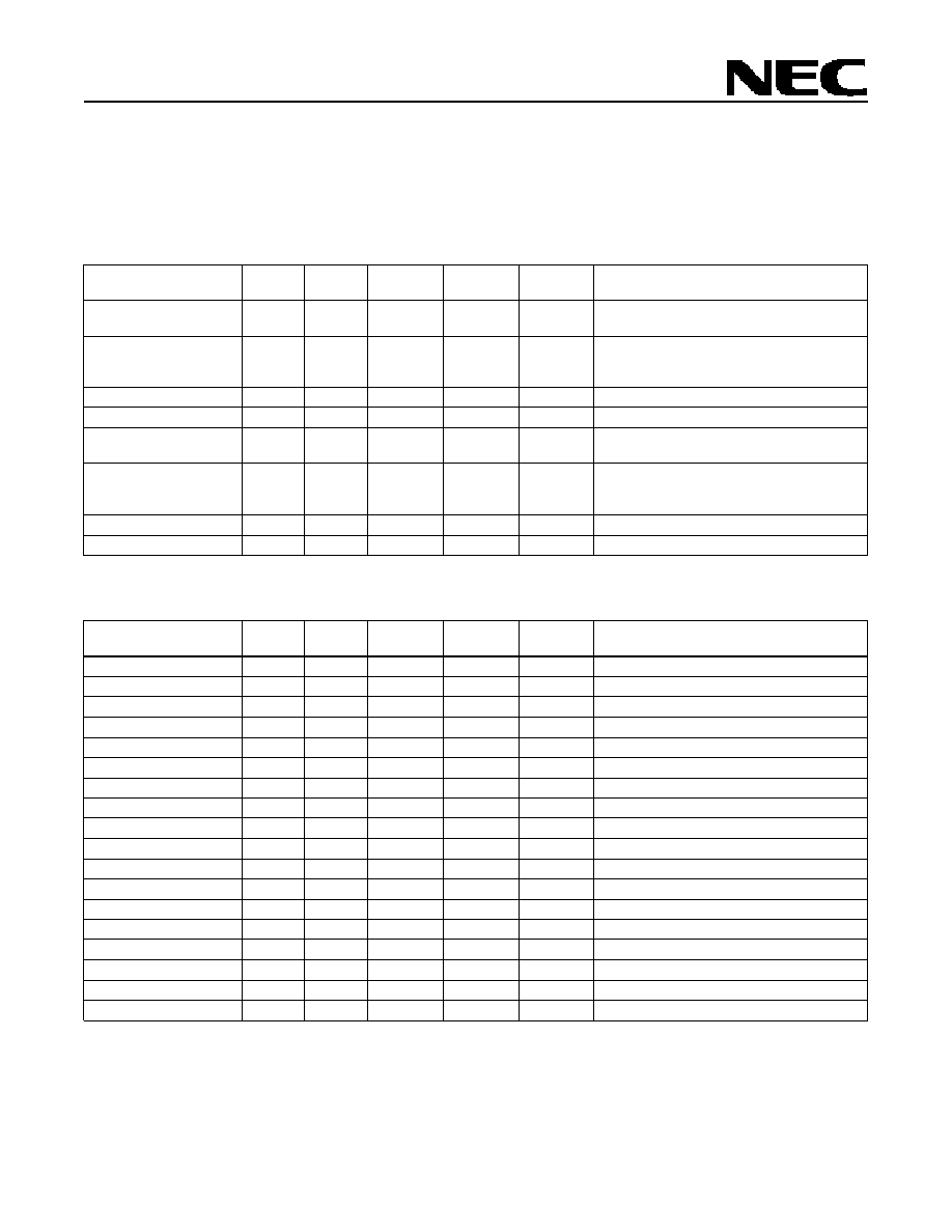
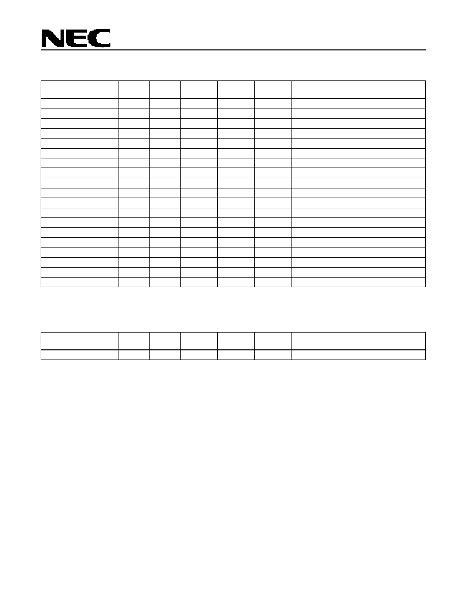
The controller has 208 signals and 51 power/ground pins, for a total of 251 pins. Table
3 through Table 4 summarize the signal functions.
Table 1: CPU Interface Signals
Signal
I/O
Reset
Value
Pullup/
Pulldown
Max. AC
Load (pF)
Max. DC
Drive (mA)
Description
EOK#
O
High
20
24
External ready; signifies that the controller is ca-
pable of accepting a processor request
EValid#
O
High
20
6
External agent valid. Indicates that the controller
is driving valid information on the SysAD and Sy-
sCmd buses
Int#
O
High
30
6
Interrupt request
MasterClock
O
Toggle
20
24
66 MHz MasterClock to CPU
NMI#
O
High
20
12
Non-maskable interrupt; asserted when a PCI
device asserts SERR#
PValid#
I
Processor valid; signifies that the V
R
4300 is driv-
ing valid information on the SysAD and SysCmd
buses
SysAD[31:0]
I/O
Hi-Z
20
6
System address/data bus
SysCmd[4:0]
I/O
Hi-Z
20
6
System command/data ID bus
Table 2: Memory Interface Signals
Signal
I/O
Reset
Value
Pullup/
Pulldown
Max. AC
Load (pF)
Max. DC
Drive (mA)
Description
BOE#
O
High
50
24
Base memory output-enable
BRAS#
O
High
50
24
Base memory row address strobe
BROMCS#
O
High
30
12
Boot ROM chip select
BWE#
O
High
50
24
Base memory write enable
MCASa[3:0]#
O
High
75
24
Column address strobe, even addresses
MCASb[3:0]#
O
High
75
24
Column address strobe, odd addresses
MRAS[3:0]#
O
High
75
24
SIMM memory row address strobes
MDa[31:0]
I/O
High
70
12
Memory data (even), boot ROM address
MDb[31:0]
I/O
High
70
12
Memory data (odd), boot ROM data
MuxAd[9:0]
I/O
Hi-Z
50K down
75
24
Multiplexed row/column address
Mux[10]
I/O
Hi-Z
75
24
Multiplexed row/column address; endian select
MuxAd[13:11]
O
Hi-Z
75
24
Multiplexed row/column address
MWE#
O
High
30
24
Boot ROM and SIMM write enable
SDCAS#
O
High
80
24
SDRAM column address strobe
SDRAS#
O
High
80
24
SDRAM row address strobe
SDCKE[3:0]
O
High
70
24
SDRAM clock enable
SDCLK[3:0]
O
High
50
24
66 MHz SDRAM clock
SDCS[1:0]#
O
High
50
24
SDRAM command select
5
a.
Compatible with PCI specification
Table 3: PCI Interface Signals
Signal
I/O
Reset
Value
Pullup/
Pulldown
Max. AC
Load (pF)
Max. DC
Drive (mA)
Description
AD[31:0]
I/O
Hi-Z
110
PCI
a
PCI A/D[31:0], multiplexed address and data bus
CBE[3:0]#
I/O
Hi-Z
110
PCI
PCI C/BE[3:0]#, bus command and byte-enables
CLK[3:0]
O
Toggle
50
PCI
PCI CLK, 33 MHz
DEVSEL#
I/O
Hi-Z
110
PCI
PCI DEVSEL#, device select
FRAME#
I/O
Hi-Z
110
PCI
PCI FRAME#, cycle frame
GNT[0]#
I/O
High
10
PCI
PCI GNT#, bus grant
GNT[3:1]#
O
High
10
PCI
PCI GNT#, bus grant
IDSEL
I
PCI IDSEL, initialization device select
INTA#
I/O
10
PCI
PCI INTA#, interrupt A
IRDY#
I/O
Hi-Z
110
PCI
PCI IRDY#, initiator ready
LOCK#
I/O
Hi-Z
10
PCI
PCI LOCK#, lock atomic operation
PAR
I/O
Hi-Z
110
PCI
PCI PAR, parity of A/D[31:0] and C/BE[3:0]#
PERR#
I/O
Hi-Z
10
PCI
PCI PERR#, parity error
REQ[0]#
I/O
10
PCI
PCI REQ#, bus request
REQ[3:1]#
I
PCI REQ#, bus request
RST#
I
PCI RST#, reset
SERR#
I/O
Hi-Z
10
PCI
PCI SERR#, system error
STOP#
I/O
Hi-Z
110
PCI
PCI STOP#, stop request from target
TRDY#
I/O
Hi-Z
110
PCI
PCI TRDY#, target ready
Table 4: Utility Signals
Signal
I/O
Reset
Value
Pullup/
Pulldown
Max. AC
Load (pF)
Max. DC
Drive (mA)
Description
REFCLK
I
Toggle
66 MHz system reference clock