PPRELIMINARY
Ver.1.0
NJW1106
- 1 -
DOLBY PRO LOGIC SURROUND DECODER
n
n
n
n
GENERAL DESCRIPTION
n
n
n
n
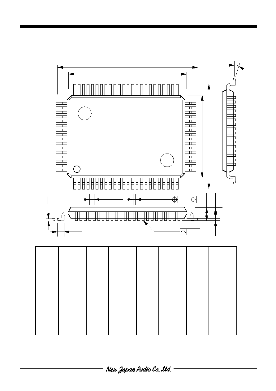
PACKAGE OUTLINE
The NJW1106 is a surround processor including all of the
necessary circuits of Dolby Pro Logic Surround decoder and
digital delay.
All of internal statuses are controlled by I
2
C BUS interface.
In addition to Dolby Pro Logic Surround function, it
performs easily other surround function such as Hall, Live,
Disco and others.
Dolby and double-D symbol are trademarks of Dolby Laboratories Licensing Corporation.
San Francisco, CA94103-4813.USA.
This device is available only to licensees of Dolby Lab.
Licensing and application information may be obtained from Dolby Lab.
Purchase of I2C components of New Japan Radio Co., Ltd. or one of its sublicensed Associated
Companies conveys a license under the Philips I2C Patent Rights to use these components in an
I2C system, provided that the system conforms to the I2C Standard Specification as defined by
Philips.
n
n
n
n
FEATURES
l
Operating Voltage : V
CC
=10V(Analog Block), V
DD
=5V(Digital Block)
l
Digital Delay on chip
l
I
2
C BUS Interface
SDA, SCL
l
Bi-CMOS Technology
l
Package Outline
QFP80, QFP100
n
n
n
n
FUNCTION
[Dolby Pro Logic Surround]
l
Automatic input balance
l
Noise sequencer
l
Adaptive matrix
l
Center channel control (Wide, Normal, Phantom, Off)
l
Modified B-type noise reduction
l
7kHz low-pass filter
l
Dolby 3 stereo mode
l
Digital time delay (15,20,25,30msec.)
[Other Surround]
l
Surround Signal Selector
(L+R, L-R, EXTIN)
l
Front mixing control
l
Digital time delay
(15,20,25,30,40,50,60msec.)
[Other Function]
l
Digital auxiliary outputs
(AUX0-AUX7)
n
n
n
n
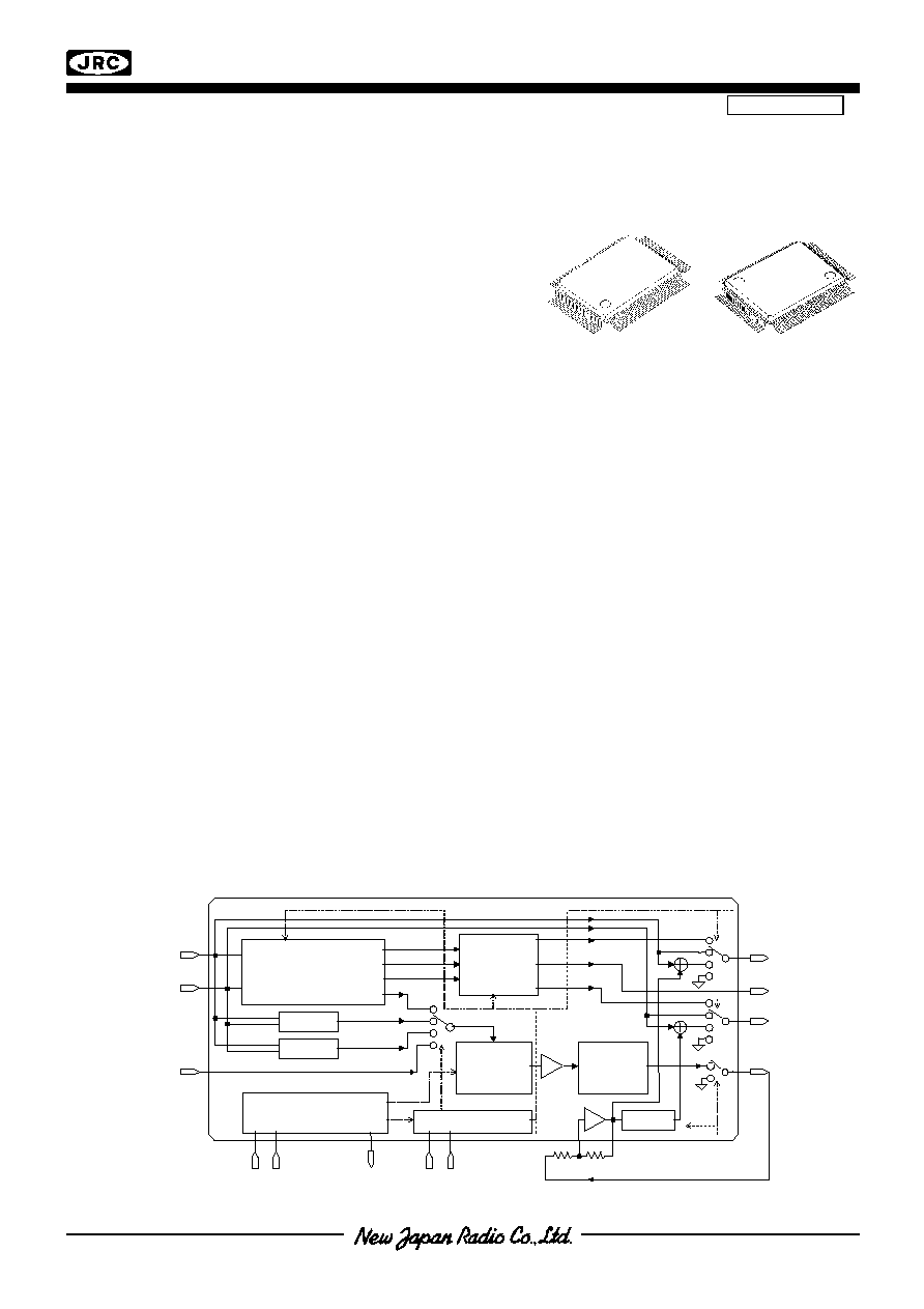
SYSTEM BLOCK DIAGRAM
EXTIN
7KHz
LPF
SW. Controller
ADD/SUB
L+R
L-R
Center Mode
Modified
BNR
I
2
C Interface
Delay
Input Autobalance
Noise Sequencer
Adaptive Matrix
RIN
LOUT
COUT
ROUT
SOUT
LIN
SDA
SCL
AUX
0
-
7
MD
1
MD
2
NJW1106FC2-80
NJW1106FC2
Ver.1.0
NJW1106
- 2 -
n
n
n
n
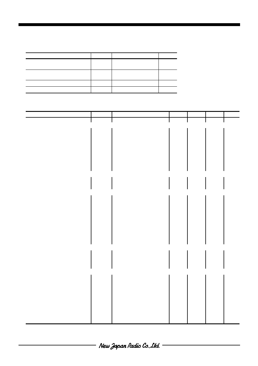
ABSOLUTE MAXIMUM RATING (Ta=25�C)
PARAMETER
SYMBOL
RATING
UNIT
Supply Voltage
V
CC
V
DD
13
6.5
V
Power Dissipation
�
P
D
(QFP80) 1.3
(QFP100) 1.3
W
Operating Temperature Range
T
opr
-40 to +85
�C
Storage Temperature Range
T
stg
-40 to +150
�C
*On board
n
n
n
n
ELECTRICAL CHARACTERISTICS (V
CC
=10V, V
DD
=5V, Ta=25�C)
PARAMETER
SYMBOL
TEST CONDITION
MIN.
TYP.
MAX.
UNIT
X
OVERALL
Supply Voltage Range
V
CC
V
DD
9
4.5
10
5
13
5.5
V
V
Supply Current
I
CC
I
DD
No Signal
No Signal
-
-
37
6
50
10
mA
mA
Reference Voltage
V
REF
No Signal
3.6
4.0
4.4
V
Threshold Voltage
V
thh
V
thl
Digital input high level
Digital input low level
0.7V
DD
0.0
-
-
V
DD
0.3V
DD
V
V
X
INPUT AUTO BALANCE
Capture Range
CPR
-
5
-
Error Correction
CER
-
4
-
X
ADAPTIVE MATRIX (0dB=300mVrms, f=1kHz at Cin Cout)
Output Level Accuracy
relative to Cch
'
Vol
L,R,S'ch.out
-0.5
0
0.5
dB
Matrix Rejection relative
MR
L,R,S'ch.out
25
40
-
dB
Headroom
HR-AM
V
CC
=9V at THD=1%
15
17
-
dB
Total Harmonic Distortion
THD-AM
L,R,C,S'ch.out at 4ch.mode
L,R,ch.out at 2ch.mode
-
-
0.05
0.002
0.2
0.1
%
%
Signal to Noise Ratio
SNAM
Rg=0,wt:CCIR-ARM at 4ch.mode
L,R,ch.out at 2ch.mode
75
93
80
100
-
-
dB
dB
X
NOISE SEQUENCER
Output Noise Level
Vno
-15.0
-12.5
-10.0
dB
Output Noise Level
Accuracy relative to Cch
'
Vno
L,R,S'ch.out
-0.5
0.0
0.5
dB
X
MODIFIED B-TYPE NOISE REDUCTION (0dB=300mVrms, f=100Hz at Sin Sout)
Voltage Gain
GV-NR
Vin=0dBd,f=100Hz
-
9.5
-
dB
Decode Responce1
DEC1
Vin=0dBd,f=1kHz
-1.6
-0.1
1.4
dB
Decode Responce2
DEC2
Vin=-15dBd,f=1.4kHz
-3.0
-1.5
0.0
dB
Decode Responce3
DEC3
Vin=-20dBd,f=1.4kHz
-4.9
-3.4
-1.9
dB
Decode Responce4
DEC4
Vin=-40dBd,f=5kHz
-6.8
-5.3
-3.8
dB
Total Harmonic Distortion
THDNR
Vin=0dBd,f=1kHz
-
0.07
0.3
%
Headroom
HRNR
V
CC
=9V at THD=1%
15
17
-
dB
Signal to Noise Ratio
SNNR
Rg=0,weightted:CCIR/ARM
73
78
-
dB