 | –≠–Ľ–Ķ–ļ—ā—Ä–ĺ–Ĺ–Ĺ—č–Ļ –ļ–ĺ–ľ–Ņ–ĺ–Ĺ–Ķ–Ĺ—ā: SM5301 | –°–ļ–į—á–į—ā—Ć:  PDF PDF  ZIP ZIP |

SM5301AS
NIPPON PRECISION CIRCUITS INC.--1
3-channel Video Buffer with Built-in Wideband Filters
OVERVIEW
The SM5301AS is a video buffer with built-in video signal bandwidth lowpass filter. The filter employs a 5-
order Butterworth lowpass filter configuration. The filter characteristics have been optimized for minimal over-
shoot and flat group delay, it has a variable cutoff frequency and guaranteed driver-stage channel gain differ-
ence and phase difference values.
FEATURES
I
Supply voltage: 5V
Ī
10%
I
VESA-standard ATSC digital TV RGB/YUV
video filters
I
2-system input/1-system output switching analog
multiplexer function
I
DC voltage level restore sync clamp function
I
Output buffer gain switching function: 0, 6dB
(input-to-output AC signal gain)
I
Channel-to-channel gain difference: 0.5dB (
Ī
5%
supply voltage variation)
I
Channel-to-channel phase difference: 3.5 degree
I
Output signal harmonic distortion (all channels):
1.5%
I
Cutoff frequency: 5.8 to 37MHz variable
I
Package: 28-pin HSOP (Pb free)
APPLICATIONS
I
Set-top boxes
I
Digital television
I
DVD players
I
Projector
ORDERING INFORMATION
PINOUT
(Top view)
PACKAGE DIMENSIONS
(Unit: mm)
Device
Package
SM5301AS
28-pin HSOP
MUXSEL
1
SYNCIN
2
VCC4
3
R
INA
/Y
INA
4
GSR1
5
R
INB
/Y
INB
6
NC
7
G
INA
/U
INA
8
GSG1
9
G
INB
/U
INB
10
NC
11
B
INA
/V
INA
12
28
27
26
25
24
23
22
21
20
19
18
17
VFC
RFC
GND4
VCC1
R
OUT
/Y
OUT
GND1
VCC2
G
OUT
/U
OUT
GND2
VCC3
B
OUT
/V
OUT
GND3
13
14
16
15
GSB1
B
INB
/V
INB
DISABLE
NC
GND
GND
1.3TYP
18.6 Ī 0.3
7.5 Ī 0.2
9.9 Ī 0.3
0.8
5.15
0.35 Ī 0.05
0.12
M
0.10
0.1 Ī 0.05
2.2 Ī 0.1
0.15 ≠ 0.05
+ 0.1
0.5 Ī 0.2
0 to 10

SM5301AS
NIPPON PRECISION CIRCUITS INC.--2
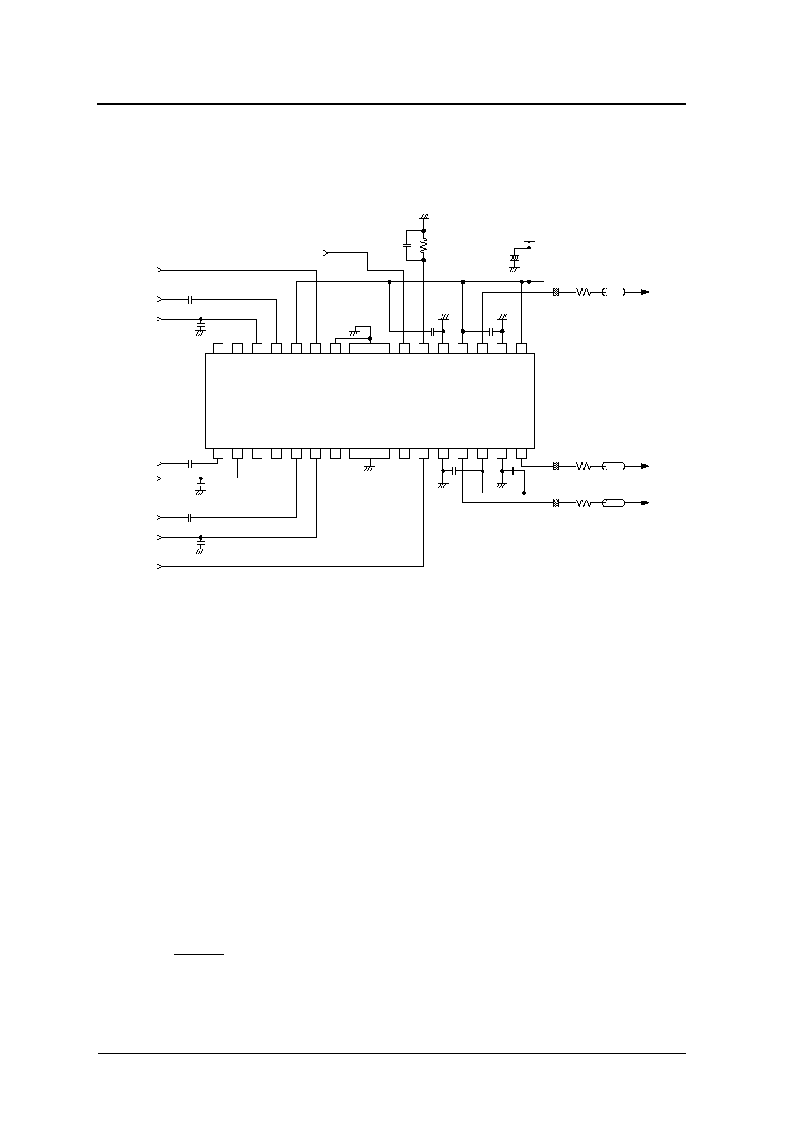
BLOCK DIAGRAM
VCC4
R
INA
/Y
INA
GSR1
R
INB
/Y
INB
VFC
GND4
VCC1
R
OUT
/Y
OUT
GND1
VCC2
GND2
VCC3
GND3
DISABLE
MUX
DC
Restore
LPF
Buffer
G
INA
/U
INA
GSG1
G
INB
/U
INB
G
OUT
/U
OUT
MUX
DC
Restore
LPF
Buffer
B
INA
/V
INA
GSB1
B
INB
/V
INB
B
OUT
/V
OUT
MUX
DC
Restore
LPF
Buffer
MUXSEL
SYNCIN
IFC
Control
RFC

SM5301AS
NIPPON PRECISION CIRCUITS INC.--3
PIN DESCRIPTION
Number
Name
I/O
Description
1
G
INA
/U
INA
I
Analog G
INA
or U
INA
signal input. Sync signal is input on SYNCIN pin.
2
GSG1
I
G
OUT
/U
OUT
output buffer gain set input
3
G
INB
/U
INB
I
Analog G
INB
or U
INB
signal input. Sync signal is input on SYNCIN pin.
4
NC
≠
No connection (leave open or connect to ground)
5
B
INA
/V
INA
I
Analog B
INA
or V
INA
signal input. Sync signal is input on SYNCIN pin.
6
GSB1
I
B
OUT
/V
OUT
output buffer gain set input
7
B
INB
/V
INB
I
Analog B
INB
or V
INB
signal input. Sync signal is input on SYNCIN pin.
8
NC
≠
No connection (leave open or connect to ground)
9
DISABLE
I
Power save function. Built-in pull-down resistor.
L: Enable
H: Disable (Output pins: R
OUT
/Y
OUT
, G
OUT
/U
OUT
, and B
OUT
/V
OUT
are high impedance.)
10
GND3
-
Analog ground
11
B
OUT
/V
OUT
O
B/V signal output
12
VCC3
-
Analog 5V supply
13
GND2
-
Analog ground
14
G
OUT
/U
OUT
O
G/U signal output
15
VCC2
-
Analog 5V supply
16
GND1
-
Analog ground
17
R
OUT
/Y
OUT
O
R/Y signal output
18
VCC1
-
Analog 5V supply
19
GND4
-
Analog ground
20
RFC
-
LPF (lowpass filter) cutoff frequency setting resistor connection
21
VFC
I
LPF (lowpass filter) cutoff frequency setting voltage input
22
MUXSEL
I
Input select signal. Built-in pull-down resistor.
L:
◊
INA
pin select
H:
◊
INB
pin select
23
SYNCIN
I
Filter channel external H-Sync signal input. Active "H". Built-in pull-down resistor.
24
VCC4
-
Analog 5V supply
25
R
INA
/Y
INA
I
Analog R
INA
or Y
INA
signal input. Sync signal is input on SYNCIN pin.
26
GSR1
I
R
OUT
/Y
OUT
output buffer gain set input
27
R
INB
/Y
INB
I
Analog R
INB
or Y
INB
signal input. Sync signal is input on SYNCIN pin.
28
NC
≠
No connection (leave open or connect to ground)

SM5301AS
NIPPON PRECISION CIRCUITS INC.--4
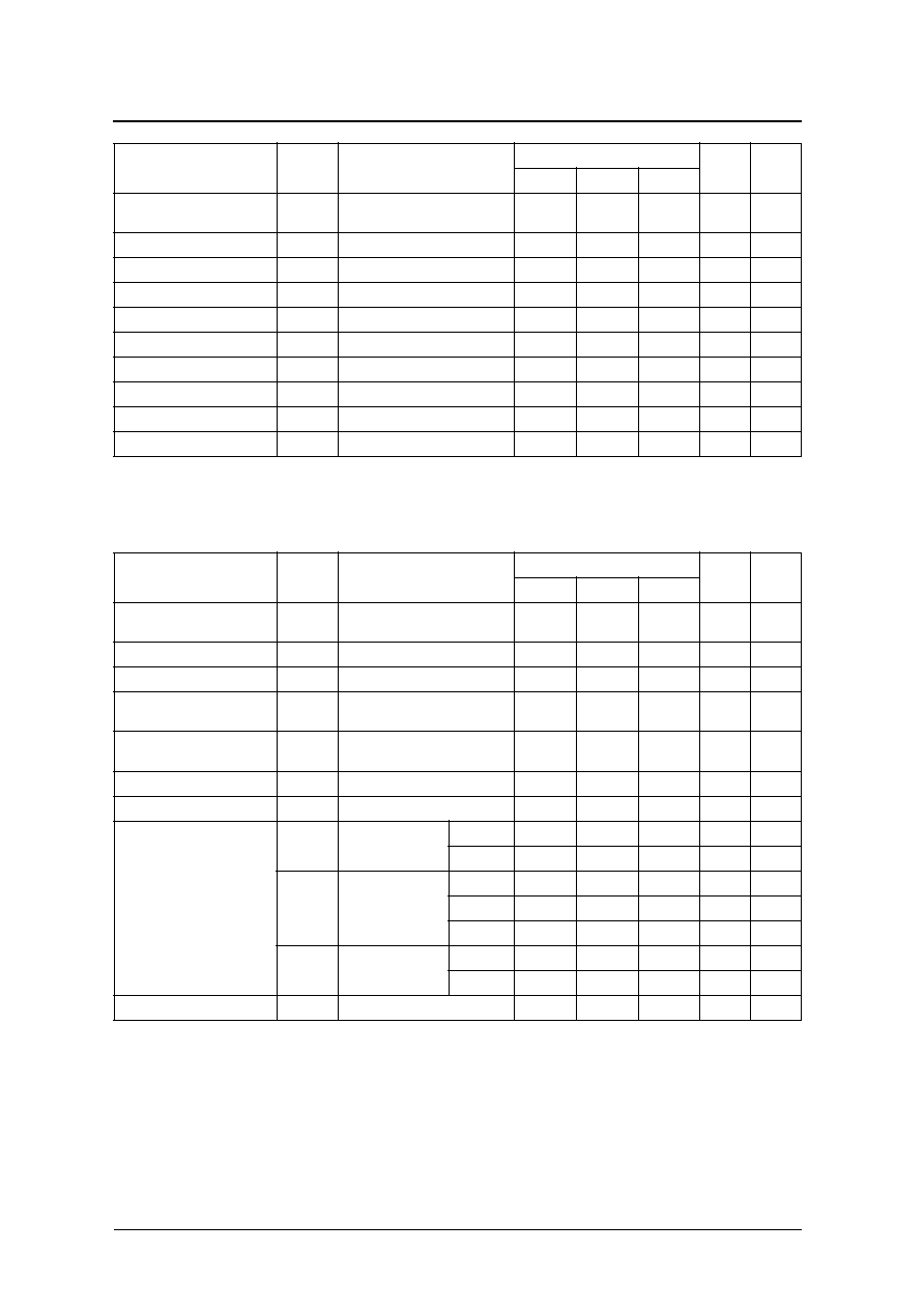
SPECIFICATIONS
Absolute Maximum Ratings
Recommended Operating Conditions
Electrical Characteristics
V
CC
= 4.5 to 5.5V, Ta = ≠ 25 to 85
į
C unless otherwise noted.
Parameter
Symbol
Rating
Unit
Supply voltage range
V
CC
-
0.3 to 7.0
V
Storage temperature range
T
stg
-
55 to
+
125
į
C
Power dissipation 1
1
1. When mounted on a substrate: mounted on a 111
◊
80
◊
1.6mm glass-epoxy substrate with 90%
copper (Cu) wiring factor, 0m/s air flow, and Ta = ≠ 25 to 70
į
C.
P
D1
1.0
W
Power dissipation 2
2
2. When mounted on a substrate: mounted on a 111
◊
80
◊
1.6mm glass-epoxy substrate with 90%
copper (Cu) wiring factor, 0m/s air flow, and Ta = 70 to 80
į
C.
P
D2
0.9
W
Parameter
Symbol
Rating
Unit
Supply voltage ranges
V
CC
4.5 to 5.5
V
Operating temperature range
Ta
≠ 25 to 85
į
C
Parameter
Symbol
Condition
Rating
Unit
Test
level
min
typ
max
Supply current 1
I
CC1
V
CC
=
5.5V, RFC = 820
to GND,
VFC
=
0.2V (fc
=
5MHz),
DISABLE
=
"L"
70
100
130
mA
I
Supply current 2
I
CC2
V
CC
=
5.5V, RFC = 820
to GND,
VFC
=
1.6V (fc
=
40MHz),
DISABLE
=
"L"
90
120
160
mA
I
Supply current 3
I
CC3
V
CC
=
5.5V, RFC = 820
to GND,
VFC
=
0.2V (fc
=
40MHz),
DISABLE
=
"H"
1
2.5
5
mA
I
Output gain error 1
A
V1
Error entered around table 1 values,
Ta = 0 to 70
į
C, V
CC
=
4.75 to 5.25V
≠ 0.5
≠
+
0.5
dB
I
Output gain error 2
A
V2
Error entered around table 1 values,
Ta = ≠ 25 to 85
į
C
≠ 1
≠
+
1
dB
I
Output voltage
V
out2
RL
=
75
to GND, 6dB gain setting
2.4
≠
≠
Vp-p
I
DISABLE-mode input impedance
(pull-down)
R
IN1
R
INA
/Y
INA
, R
INB
/Y
INB
, G
INA
/U
INA
,
G
INB
/U
INB
, B
INA
/V
INA
, B
INB
/V
INB
≠
50
≠
k
I
Clamp response time
T
clamp
Time for 90% output signal change
for 10mV input signal, C
IN
=
0.1
Ķ
F
≠
8
≠
ms
II
Maximum input amplitude
V
I
AC coupling, 6dB gain setting
≠
≠
1.4
Vp-p
I
Maximum overshoot
V
OS
2Vp-p output pulse
≠
10
≠
%
II
Maximum load capacitance
C
L
B
OUT
/V
OUT
, G
OUT
/U
OUT
, R
OUT
/Y
OUT
≠
≠
15
pF
II
Output drive load
RL
one load unit
= 150
≠
≠
2
load
I
Channel-to-channel gain
difference
dG
Between R/G/B, fc/2 [Hz]
≠
≠
0.5
dB
I
SM5301AS
NIPPON PRECISION CIRCUITS INC.--5
Filter Characteristics
V
CC
= 4.5 to 5.5V, Ta = ≠ 25 to 85
įC unless otherwise noted.
Test level
I : 100% of products tested at Ta = + 25
įC.
II : Guaranteed as result of design and characteristics evaluation.
Channel-to-channel phase
difference
d
Between R/G/B, fc/2 [Hz]
≠
3.5
≠
degree
II
Output harmonic distortion
T
HD
Vout
= 2Vp-p, f = 1MHz
≠
1.5
≠
%
II
Power supply rejection ratio
PSRR
V
CC
= 0.5Vp-p, f = 100kHz
≠
35
≠
dB
II
Output short-circuit current
I
SC
≠
≠
100
mA
II
Logic HIGH-level input voltage 1
V
IH1
DISABLE, MUXSEL, SYNCIN
2.5
≠
≠
V
I
Logic LOW-level input voltage 1
V
IL1
DISABLE, MUXSEL, SYNCIN
≠
≠
1.0
V
I
Logic HIGH-level input voltage 2
V
IH2
GSB1, GSG1, GSR1
V
CC
- 0.5
≠
≠
V
I
Logic LOW-level input voltage 2
V
IL2
GSB1, GSG1, GSR1
≠
≠
0.5
V
I
Logic pull-up resistance
R
IN2
GSB1, GSG1, GSR1
≠
40
≠
k
I
Logic pull-down resistance
R
IN3
DISABLE, MUXSEL, SYNCIN
≠
50
≠
k
I
Parameter
Symbol
Condition
Rating
Unit
Test
level
min
typ
max
Cutoff frequency adjustment
range
F
C
Ta=25
įC (see figure 1)
5.8
≠
37
MHz
I
Cutoff frequency error
F
C
Ta
= 25įC, V
CC
= 5.0V
≠
≠
Ī 20
%
I
4fc attenuation
f
SB
fIN
4fc
≠
50
≠
dB
II
Output noise characteristic
V
NOISE
10kHz to 40MHz, 6dB output gain
setting
≠
1.0
≠
mV
RMS
II
Crosstalk
X
TALK
Between 2 channels with input
0.5Vp-p 1MHz
≠
- 47
≠
dB
II
Multiplexer crosstalk
X
TALK
Between MUX A
-B
≠
- 49
≠
dB
II
Channel-to-channel group delay
T
PD
Each input = 500kHz
≠
10
≠
ns
II
Group delay variation
T
PD1
Fc
= 6.7MHz
(500kHz)
to 3.58MHz
≠
9
≠
ns
II
to 4.43MHz
≠
15
≠
ns
II
T
PD2
Fc
= 24MHz
(500kHz)
to 3.58MHz
≠
1
≠
ns
II
to 4.43MHz
≠
1
≠
ns
II
to 10MHz
≠
2
≠
ns
II
T
PD3
Fc
= 36MHz
(1MHz)
to 10MHz
≠
0.5
≠
ns
II
to 30MHz
≠
5
≠
ns
II
VFC input voltage range
VFC
0.2
≠
1.6
V
I
Parameter
Symbol
Condition
Rating
Unit
Test
level
min
typ
max
SM5301AS
NIPPON PRECISION CIRCUITS INC.--6
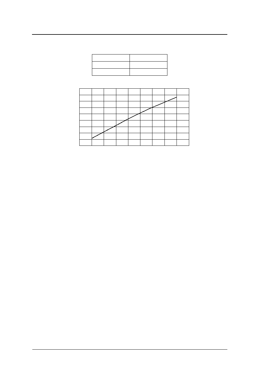
Table 1. Output buffer gain control
GS
◊1
Gain [dB]
GND
0
VCC or Open
6
RFC: 820
to GND
Figure 1. VFC vs. cutoff frequency
0
5
10
15
20
25
30
35
40
45
0.0
0.2
0.4
0.6
0.8
1.0
1.2
1.4
1.6
1.8
VFC [V]
fc [MHz]
SM5301AS
NIPPON PRECISION CIRCUITS INC.--7
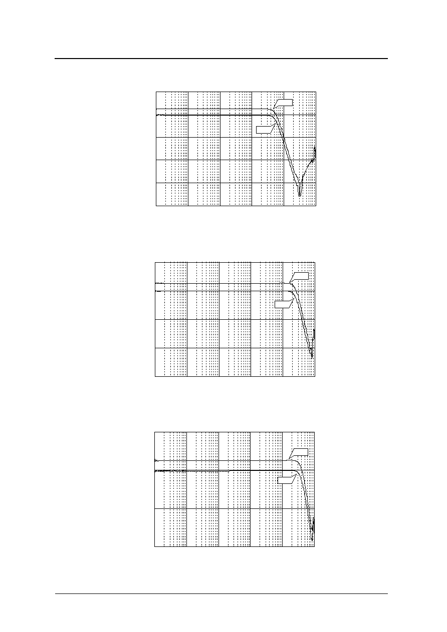
Figure 2. Frequency response (VFC = 0.2V)
Figure 3. Frequency response (VFC = 1.0V)
Figure 4. Frequency response (VFC = 1.6V)
≠8.00E+01
≠6.00E+01
≠4.00E+01
≠2.00E+01
0.00E+00
2.00E+01
1.00E+03
1.00E+04
1.00E+05
1.00E+06
1.00E+07
1.00E+08
Gain [dB]
Frequency [Hz]
6dB
0dB
≠6.00E+01
≠4.00E+01
≠2.00E+01
0.00E+00
2.00E+01
1.00E+03
1.00E+04
1.00E+05
1.00E+06
1.00E+07
1.00E+08
Gain [dB]
Frequency [Hz]
6dB
0dB
-4.00E+01
-2.00E+01
0.00E+00
2.00E+01
1.00E+03
1.00E+04
1.00E+05
1.00E+06
1.00E+07
1.00E+08
Gain [dB]
Frequency [Hz]
6dB
0dB

SM5301AS
NIPPON PRECISION CIRCUITS INC.--8
Adjusting the Cutoff Frequency
Constant-voltage control 1
Cutoff frequency control using a reference voltage VR generated by voltage divider formed by R1 and R2.
Constant-voltage control 2
Cutoff frequency control by adjusting the resistance connected to RFC.
PWM control
Cutoff frequency control by smoothing the PWM signal, using R1 and C1, input to VFC.
When VFC = 0.2V V
DD
= 3.3V, 6% duty drive
V
DD
= 5.0V, 4% duty drive
When VFC = 1.6V V
DD
= 3.3V, 48% duty drive
V
DD
= 5.0V, 32% duty drive
Note: The resistor connected to RFC can affect the cutoff frequency response, so a high-precision component
should be used. It is recommended to set the RC filter cutoff frequency to < fc/100 of the PWM wave-
form frequency.
VFC
VR
RFC
R1
R2
VFC
VR
RFC
VFC
RFC
R1
C1
PWM

SM5301AS
NIPPON PRECISION CIRCUITS INC.--9
Resistor switch control
The VFC voltage can be controlled using multi-logic voltage levels switching inputs to a voltage divider resis-
tor network.
The VFC voltage is determined by the logic voltage (V1, V2, V3) and the corresponding voltage divider resis-
tor network.
VFC
RFC
R1
R0
V1
V2
V3
R2
R3
SM5301AS
NIPPON PRECISION CIRCUITS INC.--10
TYPICAL APPLICATION CIRCUITS
ATSC Digital TV Application
(*1) Pins without an input signal, set by NUXSEL, should be left open or tied to GND.
(*2) Connect 4
◊ 0.1ĶF capacitor between the supply pins close to the IC.
(*3) Connect a 47
ĶF capacitor between the supply pins close to the IC.
(*4) GS
◊1 are 3-level pins. Connect a capacitor if an error occurs due to external noise. Also, if open-circuit,
the internal impedance and external capacitance (C) form an RC network. When power is applied, the
open-circuit potential rises with time constant
= C ◊ 10k (sec).
(*5) Printed circuit board supply wiring
I
If the supply is used for other digital circuits, there is a possibility that noise will be introduced. Accord-
ingly, these circuits should be connected to the application's analog supply.
I
Ground-plane wiring should be performed, as much as possible, to provide low GND line impedance.
I
If ground-plane wiring up to the GND pins is difficult, the ground plane should be as close to the IC as
possible with a separate wire to each GND pin.
Input Capacitor and Cutoff Frequency
The capacitor connected to pins R
INA
/Y
INA
, R
INB
/Y
INB
, G
INA
/U
INB
, G
INB
/U
INB
, B
INA
/V
INA
, and B
INB
/V
INB
forms a highpass filter (HPF) with the internal impedance.
The HPF cutoff frequency is given by the following equation.
(C: input capacitance, R: signal input impedance = 9.3k
)
MUXSEL
SYNCIN
VCC4
R
INA
/Y
INA
GSR1
R
INB
/Y
INB
NC
G
INA
/U
INA
GSG1
G
INB
/U
INB
NC
B
INA
/V
INA
VFC
RFC
GND4
VCC1
R
OUT
/Y
OUT
GND1
VCC2
G
OUT
/U
OUT
GND2
VCC3
B
OUT
/V
OUT
GND3
GSB1
B
INB
/V
INB
DISABLE
NC
820
Cut-off
control voltage
+
+5V
(*2)
(*3)
B
IN
/V
IN
1.0
ĶF
G
IN
/U
IN
1.0
ĶF
(*1)
(*4)
GSB1
DISABLE
(*1)
(*2)
220
ĶF
B/V
+
75
220
ĶF
R/Y
+
75
(*4)
GSG1
(*4)
GSR1
R
IN
/Y
IN
1.0
ĶF
SYNC
(*1)
(*2)
(*2)
220
ĶF
G/U
+
75
fc =
1
2
CR
SM5301AS
NIPPON PRECISION CIRCUITS INC.--11
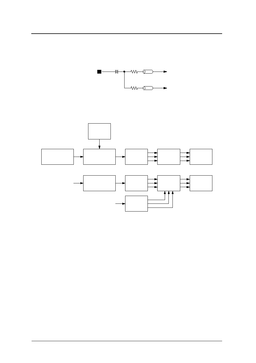
2-load Output Connection
R
OUT
/Y
OUT
output 2-load connection (similarly for G
OUT
/U
OUT
, B
OUT
/V
OUT
outputs)
Digital TV Receiver and HDTV Decoder Box
R
OUT
/Y
OUT
220
ĶF
R/Y1
+
75
R/Y2
75
MPEG2
Transport/Decoder
HDTV
Decoder/Display
Processor
Graphic
Processor
D to A
Convertor
SM5301
DIGITAL TV
Video Decoder
and
Display Processor
D to A
Convertor
SM5301
RGB
MONITOR
Graphic
Processor
CAMERA
DVD-ROM MEMORY

SM5301AS
NIPPON PRECISION CIRCUITS INC.--12
NC0202BE
2003.05
Please pay your attention to the following points at time of using the products shown in this document.
The products shown in this document (hereinafter "Products") are not intended to be used for the apparatus that exerts harmful influence on
human lives due to the defects, failure or malfunction of the Products. Customers are requested to obtain prior written agreement for such
use from NIPPON PRECISION CIRCUITS INC. (hereinafter "NPC"). Customers shall be solely responsible for, and indemnify and hold NPC
free and harmless from, any and all claims, damages, losses, expenses or lawsuits, due to such use without such agreement. NPC reserves
the right to change the specifications of the Products in order to improve the characteristic or reliability thereof. NPC makes no claim or
warranty that the contents described in this document dose not infringe any intellectual property right or other similar right owned by third
parties. Therefore, NPC shall not be responsible for such problems, even if the use is in accordance with the descriptions provided in this
document. Any descriptions including applications, circuits, and the parameters of the Products in this document are for reference to use the
Products, and shall not be guaranteed free from defect, inapplicability to the design for the mass-production products without further testing
or modification. Customers are requested not to export or re-export, directly or indirectly, the Products to any country or any entity not in
compliance with or in violation of the national export administration laws, treaties, orders and regulations. Customers are requested
appropriately take steps to obtain required permissions or approvals from appropriate government agencies.
NIPPON PRECISION CIRCUITS INC.
4-3, Fukuzumi 2-chome, Koto-ku,
Tokyo 135-8430, Japan
Telephone: +81-3-3642-6661
Facsimile: +81-3-3642-6698
http://www.npc.co.jp/
Email: sales
@
npc.co.jp