 | –≠–ª–µ–∫—Ç—Ä–æ–Ω–Ω—ã–π –∫–æ–º–ø–æ–Ω–µ–Ω—Ç: SM5839A | –°–∫–∞—á–∞—Ç—å:  PDF PDF  ZIP ZIP |
SM5839A
NIPPON PRECISION CIRCUITS--1
NIPPON PRECISION CIRCUITS INC.
High-Speed Variable-Length Shift Register
OVERVIEW
The SM5839A is an 8-bit variable-length shift
resister. The input pins can be configured to function
as a 2 to 128-step shift resister. The shift clock has a
maximum frequency of 54 MHz, making it ideal for
high-speed digital signal processing.
FEATURES
s
2 to 128-step selectable variable-length shift
resister
s
Static circuitry
s
8-bit (byte) word length
s
Selectable circulating/non-circulating storage
s
54 MHz maximum operating clock frequency
(standard-voltage specification)
s
Supply voltage
∑ 5.0
±
0.5 V (standard-voltage specification)
∑ 2.7 to 4.5 V (low-voltage specification)
s
TTL-compatible input/outputs
s
Molybdenum-gate CMOS
s
Package
∑ 28-pin DIP (SM5839AP)
∑ 28-pin VSOP (SM5839AV)
PINOUT
Top view
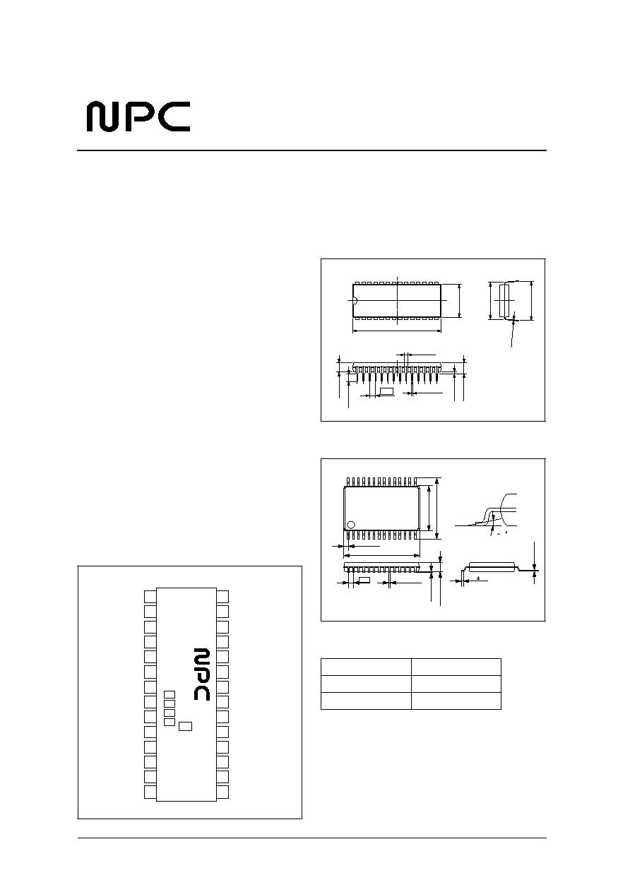
PACKAGE DIMENSIONS
Unit: mm
28-pin DIP (SM5839AP)
28-pin VSOP (SM5839AV)
ORDERING INFORMATION
1
DIN0
2
DIN1
3
DIN2
4
DIN3
5
DIN4
6
DIN5
7
DIN6
8
DIN7
9
S6
10
S5
11
S4
12
S3
13
CLK
14
VSS
15
S2
16
S1
17
S0
18
DOUT7
19
DOUT6
20
DOUT5
21
DOUT4
22
DOUT3
23
DOUT2
24
DOUT1
25
DOUT0
26
OE
27
ENRC
28
VDD
SM5839A
Device
Package
SM5839AP
28-pin DIP
SM5839AV
28-pin VSOP
36.83
±
0.1
13.72
±
0.1
15.56
±
0.3
16.38
±
0.6
1.52
±
0.05
2.54
3.18
±
0.1
0.46
±
0.05
3.81
±
0.1
0.83
±
0.3
4.64
±
0.3
0.25
±
0.05
0.5755 TYP.
0.65
0.15
-
0.05
+
0.1
5.6
±
0.2
7.6
±
0.2
9.8
±
0.2
0.5 0.2
0.22
-
0.05
+
0.1
0.10
±
0.05
1.15
±
0.1
0 10

SM5839A
NIPPON PRECISION CIRCUITS--2
BLOCK DIAGRAM
PIN DESCRIPTION
Number
Name
I/O
1
Description
1
DIN0
Ip
Data input 0
2
DIN1
Ip
Data input 1
3
DIN2
Ip
Data input 2
4
DIN3
Ip
Data input 3
5
DIN4
Ip
Data input 4
6
DIN5
Ip
Data input 5
7
DIN6
Ip
Data input 6
8
DIN7
Ip
Data input 7
9
S6
Ip
Register length select control 6
10
S5
Ip
Register length select control 5
11
S4
Ip
Register length select control 4
12
S3
Ip
Register length select control 3
13
CLK
I
Clock input
14
VSS
≠
Ground
15
S2
Ip
Register length select control 2
16
S1
Ip
Register length select control 1
17
S0
Ip
Register length select control 0
18
DOUT7
O
Data output 7
19
DOUT6
O
Data output 6
20
DOUT5
O
Data output 5
ENRC
VDD
DOUT0
to
DOUT7
S0 to S6
OE
VSS
CLK
DIN0
to
DIN7
Variable shift
register block
Output
buffer
Multiplexer
7
8
8
8
8
8
Write address pointer
Read address pointer

SM5839A
NIPPON PRECISION CIRCUITS--3
SPECIFICATIONS
Absolute Maximum Ratings
V
SS
= 0 V
Recommended Operating Conditions
V
SS
= 0 V
DC Characteristics
Standard-voltage specification: V
DD
= 5.0
±
0.5 V, V
SS
= 0 V, T
a
=
-
20 to 70
∞
C
1. Ip = input pin with pull-up resistor, I = input pin, O = output pin. All outputs are 3-state pins.
21
DOUT4
O
Data output 4
22
DOUT3
O
Data output 3
23
DOUT2
O
Data output 2
24
DOUT1
O
Data output 1
25
DOUT0
O
Data output 0
26
OE
Ip
Output enable
27
ENRC
Ip
Circulating/non-circulating control
28
VDD
≠
Supply voltage
Parameter
Symbol
Rating
Unit
Supply voltage range
V
DD
-
0.3 to 7.0
V
Input voltage range
V
IN
V
SS
-
0.3 to V
DD
+ 0.3
V
Storage temperature range
T
stg
-
40 to 125
∞
C
Power dissipation
P
D
330
mW
Soldering temperature
T
sld
255
∞
C
Soldering time
t
sld
10
s
Parameter
Symbol
Condition
Rating
Unit
min
typ
max
Supply voltage range
V
DD
Standard-voltage
specification
4.5
≠
5.5
V
Low-voltage specification
2.7
≠
4.5
V
Operating temperature
T
opr
-
20
≠
70
∞
C
Parameter
Symbol
Condition
Rating
Unit
min
typ
max
Standby current consumption
I
ST
≠
≠
50
µ
A
Operating current consumption
I
DD
OE = 0 V, f
CLK
= 54 MHz
≠
30
50
mA
Input voltage
1
V
IH
2.4
≠
≠
V
V
IL
≠
≠
0.5
Output voltage
2
V
OH
I
OH
=
-
0.4 mA
2.5
≠
≠
V
V
OL
I
OL
= 1.6 mA
≠
≠
0.4
Input current
3
I
IL
V
IN
= 0 V
≠
100
200
µ
A
Number
Name
I/O
1
Description
SM5839A
NIPPON PRECISION CIRCUITS--4
Low-voltage specification: V
DD
= 3.0
±
0.3 V, V
SS
= 0 V, T
a
=
-
20 to 70
∞
C
AC Characteristics
Standard-voltage specification: V
DD
= 5.0
±
0.5 V, V
SS
= 0 V, T
a
=
-
20 to 70
∞
C
1. All inputs (CLK, DIN0 to DIN7, S0 to S6, OE, ENRC)
2. All outputs (DOUT0 to DOUT7)
3. Inputs DIN0 to DIN7, S0 to S6, OE, ENRC
4. Input CLK only
1. All inputs (CLK, DIN0 to DIN7, S0 to S6, OE, ENRC)
2. All outputs (DOUT0 to DOUT7)
3. Inputs DIN0 to DIN7, S0 to S6, OE, ENRC
4. Input CLK only
Input leakage current
4
I
LL
V
IN
= 0 V
≠
≠
1
µ
A
Input leakage current
1
I
LH
V
IN
= V
DD
≠
≠
1
µ
A
Output high-impedance leakage
current
2
I
ZH
V
OUT
= V
DD
≠
≠
5
µ
A
I
ZL
V
OUT
= 0 V
≠
≠
5
Parameter
Symbol
Condition
Rating
Unit
min
typ
max
Standby current consumption
I
ST
≠
≠
50
µ
A
Operating current consumption
I
DD
OE = 0 V, f
CLK
= 20 MHz
≠
10
20
mA
Input voltage
1
V
IH
2.0
≠
≠
V
V
IL
≠
≠
0.5
Output voltage
2
V
OH
I
OH
=
-
0.4 mA
2.0
≠
≠
V
V
OL
I
OL
= 1.6 mA
≠
≠
0.8
Input current
3
I
IL
V
IN
= 0 V
≠
30
60
µ
A
Input leakage current
4
I
LL
V
IN
= 0 V
≠
≠
1
µ
A
Input leakage current
1
I
LH
V
IN
= V
DD
≠
≠
1
µ
A
Output high-impedance leakage
current
2
I
ZH
V
OUT
= V
DD
≠
≠
5
µ
A
I
ZL
V
OUT
= 0 V
≠
≠
5
Parameter
Symbol
Condition
Rating
Unit
min
typ
max
CLK clock frequency
f
CLK
≠
≠
54
MHz
CLK rise time
t
CR
≠
≠
100
ns
CLK fall time
t
CF
≠
≠
100
ns
CLK clock pulsewidth
t
WH
7
≠
≠
ns
DIN0 to DIN7, ENRC input setup time
t
S1
2
≠
≠
ns
S0 to S6 input setup time
t
S2
12
≠
≠
ns
DIN0 to DIN7, ENRC input hold time
t
H1
2
≠
≠
ns
S0 to S6 input hold time
t
H2
0
≠
≠
ns
DOUT0 to DOUT7 output data delay
time
t
D
Output load circuit 1
≠
≠
18
ns
Parameter
Symbol
Condition
Rating
Unit
min
typ
max
SM5839A
NIPPON PRECISION CIRCUITS--5
Low-voltage specification: V
DD
= 2.7 to 4.5 V, V
SS
= 0 V, T
a
=
-
20 to 70
∞
C
Output load circuit 1
Output load circuit 2
DOUT0 to DOUT7 output data hold
time
t
OH
Output load circuit 1
4
≠
≠
ns
DOUT0 to DOUT7 output enable
delay time
t
OEN0
, t
OEN1
Output load circuit 2
≠
≠
18
ns
DOUT0 to DOUT7 output disable
delay time
t
ODE0
, t
ODE1
Output load circuit 2
≠
≠
18
ns
Parameter
Symbol
Condition
Rating
Unit
min
typ
max
CLK clock frequency
f
CLK
≠
≠
20
MHz
CLK rise time
t
CR
≠
≠
100
ns
CLK fall time
t
CF
≠
≠
100
ns
CLK clock pulsewidth
t
WH
10
≠
≠
ns
DIN0 to DIN7, ENRC input setup time
t
S1
5
≠
≠
ns
S0 to S6 input setup time
t
S2
22
≠
≠
ns
DIN0 to DIN7, ENRC input hold time
t
H1
2
≠
≠
ns
S0 to S6 input hold time
t
H2
0
≠
≠
ns
DOUT0 to DOUT7 output data delay
time
t
D
Output load circuit 1
≠
≠
35
ns
DOUT0 to DOUT7 output data hold
time
t
OH
Output load circuit 1
7
≠
≠
ns
DOUT0 to DOUT7 output enable
delay time
t
OEN0
, t
OEN1
Output load circuit 2
≠
≠
35
ns
DOUT0 to DOUT7 output disable
delay time
t
ODE0
, t
ODE1
Output load circuit 2
≠
≠
35
ns
Parameter
Symbol
Condition
Rating
Unit
min
typ
max
Output pin
40pF
Output pin
40pF
500
0V (t
ODE1
, t
OEN1
)
2.6V (t
ODE0
, t
OEN0
) standard voltage type
1.6V (t
ODE0
, t
OEN0
) Low voltage type

SM5839A
NIPPON PRECISION CIRCUITS--6
TIMING DIAGRAM
CLK
DIN to DIN7
S0 to S6
OE
DOUT0 to DOUT7
1.5V
1.5V
1.5V
1.5V
1.5V
1.5V
t
CR
t
CF
90%
10%
Invalid
t
WH
1/f
CLK
t
H1
t
H1
t
S1
t
S1
t
S1
t
H1
t
H2
t
H2
t
S2
t
ODE
V
V
Hi-Z
t
OEN
V=0.1V
DD
(t
ODE1
)
(t
ODE0
)
(t
OEN1
)
(t
OEN0
)
t
D
t
OH
ENRC
SM5839A
NIPPON PRECISION CIRCUITS--7
FUNCTIONAL DESCRIPTION
Initialization
After power is first applied, up to a maximum of 128
input data cycles are considered invalid. However,
any cycle that momentarily sets the register length to
2 steps (by setting S1 to S6 all LOW) and then to the
desired value is considered to be the first valid cycle.
Resister Length Select
The S0 to S6 inputs set the register length (L) to the
decimal-value given by the following equation using
positive logic (HIGH = 1 and LOW = 0).
L = 64
(S6) + 32
(S5) + 16
(S4) + 8
(S3) +
4
(S2) + 2
(S1) + (S0) + 1
Clock and Output Control
Length
S6
S5
S4
S3
S2
S1
S0
128
1
1
1
1
1
1
1
127
1
1
1
1
1
1
0
126
1
1
1
1
1
0
1
125
1
1
1
1
1
0
0
66
1
0
0
0
0
0
1
65
1
0
0
0
0
0
0
64
0
1
1
1
1
1
1
3
0
0
0
0
0
1
0
2
0
0
0
0
0
0
◊
Input
Shift register
Output
ENRC
CLK
OE
DOUT0 to DOUT7
◊
◊
L
≠
High impedance
◊
◊
H
≠
Enabled
H
L
H
◊
Circulating
≠
L
L
H
◊
Non-circulating
≠

SM5839A
NIPPON PRECISION CIRCUITS--8
NIPPON PRECISION CIRCUITS INC. reserves the right to make changes to the products described in this data sheet in order to
improve the design or performance and to supply the best possible products. Nippon Precision Circuits Inc. assumes no responsibility for
the use of any circuits shown in this data sheet, conveys no license under any patent or other rights, and makes no claim that the circuits
are free from patent infringement. Applications for any devices shown in this data sheet are for illustration only and Nippon Precision Cir-
cuits Inc. makes no claim or warranty that such applications will be suitable for the use specified without further testing or modification.
The products described in this data sheet are not intended to use for the apparatus which influence human lives due to the failure or mal-
function of the products. Customers are requested to comply with applicable laws and regulations in effect now and hereinafter, including
compliance with export controls on the distribution or dissemination of the products. Customers shall not export, directly or indirectly, any
products without first obtaining required licenses and approvals from appropriate government agencies.
NIPPON PRECISION CIRCUITS INC.
4-3, 2-chome Fukuzumi
Koto-ku, Tokyo 135-8430, Japan
Telephone: 03-3642-6661
Facsimile: 03-3642-6698
NC9615BE 1999.10
NIPPON PRECISION CIRCUITS INC.