CLC005
ITU-T G.703 Cable Driver with Adjustable Outputs
General Description
National's Comlinear CLC005 is a monolithic, high-speed
cable driver designed for the ITU-T G.703 serial digital data
transmission standard. The CLC005 drives 75
transmis-
sion lines (Belden 8281 or equivalent) at data rates from DC
to over 622 Mbps. Output signal waveforms produced by the
CLC005 comply with G.703 specifications. Controlled output
rise and fall times (650 ps typical) minimize transition-
induced jitter. The output voltage swing, typically 2.0V, set by
an accurate, low-drift internal bandgap reference, delivers a
1.0V swing to back-matched and terminated 75
cable. Out-
put swing is adjustable from 0.7 V
p-p
to 2.2 V
p-p
using exter-
nal resistors.
The CLC005's class AB output stage consumes less power
than other designs, 185 mW with both outputs terminated,
and requires no external bias resistors. The differential in-
puts accept a wide range of digital signals from 200 mV
p-p
to
G.703 levels within the specified common-mode limits. All
this make the CLC005 an excellent general purpose high
speed driver for digital applications.
The CLC005 is powered from a single +5V or -5.2V supply
and comes in an 8-pin SOIC package.
Key Specifications
n
650 ps rise and fall times
n
Data rates to 622 Mbps
n
200 mV differential input
n
Low residual jitter (25 ps
pp
)
Features
n
No external pull-down resistors
n
Adjustable output amplitude
n
Differential input and output
n
Low power dissipation
n
Single +5V or -5.2V supply
Applications
n
ITU-T G.703, Sonet/SDH, and ATM compatible driver
n
Digital routers and distribution amplifiers
n
Coaxial cable driver for digital transmission line
n
Twisted pair driver
n
Buffer applications
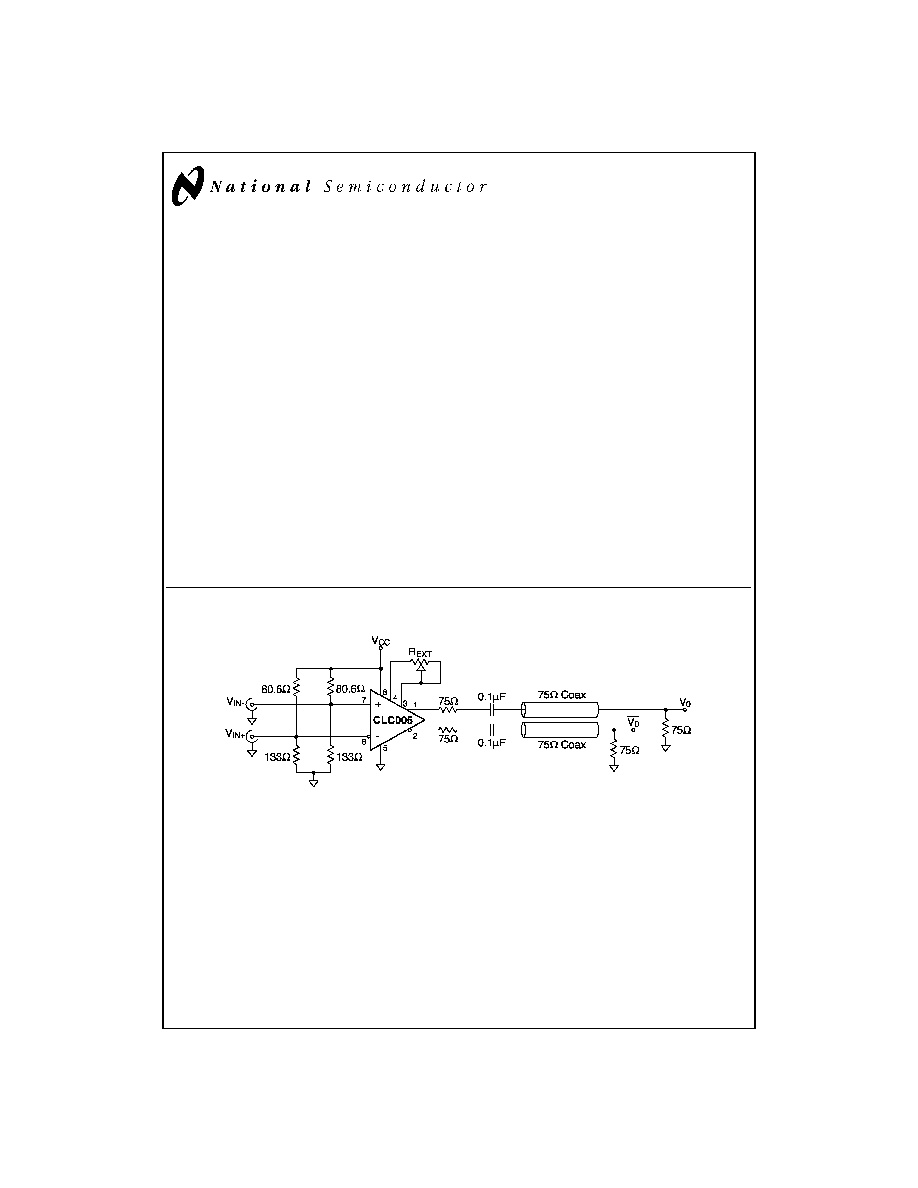
Typical Application
DS100144-2
August 1998
CLC005
ITU-T
G.703
Cable
Driver
with
Adjustable
Outputs
� 1998 National Semiconductor Corporation
DS100144
www.national.com
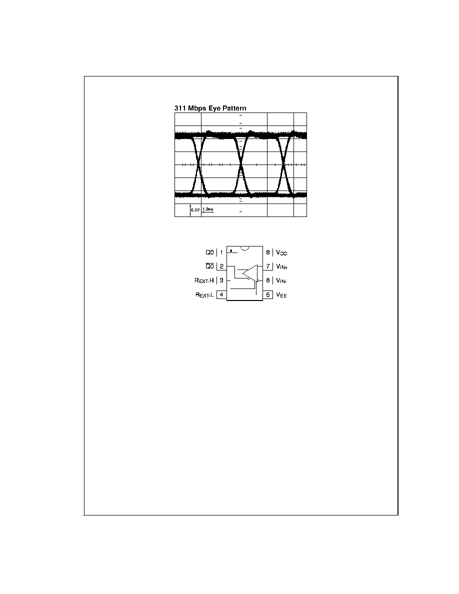
Typical Performance Characteristic
Connection Diagram (8-Pin SOIC)
DS100144-1
DS100144-3
Order Number CLC005AJE
See NS Package Number M08A
www.national.com
2

Absolute Maximum Ratings
(Note 1)
If Military/Aerospace specified devices are required,
please contact the National Semiconductor Sales Office/
Distributors for availability and specifications.
Supply Voltage
6V
Output Current
30 mA
Maximum Junction Temperature
+125�C
Storage Temperature Range
-65�C to +150�C
Lead Temperature
(Soldering 10 seconds)
+300�C
ESD Rating (Human Body Model)
1000V
Package Thermal Resistance
JA
Surface Mount AJE
125�C/W
JC
Surface Mount AJE
105�C/W
Reliability Information
Transistor count
72
MTTF
254 Mhr
Recommended Operating
Conditions
Supply Voltage Range (V
CC
�V
EE
)
+4.5V to +5.5V
Electrical Characteristics
(V
CC
= 0V, V
EE
= -5V; unless otherwise specified).
Parameter
Condition
Typ
+25�C
Min/Max
+25�C
Min/Max
0�C to
+70�C
Min/Max
-40�C to
+85�C
Units
STATIC DC PERFORMANCE
Supply Current, Loaded
150
@
270 Mbps
(Notes 5, 7)
37
-
-
-
mA
Supply Current, Unloaded
(Note 3)
34
28/37
26/39
26/39
mA
Output HIGH Voltage (V
OH
)
(Note 3)
-1.7
-2.0/1.4
-2.0/1.4
-2.0/1.4
V
Output LOW Voltage (V
OL
)
(Note 3)
-3.7
-4.0/3.4
-4.0/3.4
-4.0/3.4
V
Input Bias Current
(Note 4)
10
30
50
50
�A
Output Swing
R
EXT
=
(Note 3)
2.0
1.86/2.14
1.86/2.14
1.86/2.14
V
Output Swing
R
EXT
= 10 k
(Note 5)
1.30
-
-
-
V
Common Mode Input Range Upper Limit
-0.7
-0.8
-0.8
-0.8
V
Common Mode Input Range Lower Limit
-2.6
-2.5
-2.5
�2.5
V
Minimum Differential Input Swing (Note 5)
200
200
200
200
mV
Power Supply Rejection Ratio (Note 3)
26
20
20
20
dB
AC PERFORMANCE
Output Rise and Fall Time
(Notes 3, 6, 7)
650
425/825
400/850
400/850
ps
Overshoot
(Note 5)
5
%
Propagation Delay
(Note 5)
1.0
ns
Duty Cycle Distortion
(Note 5)
50
ps
Residual Jitter
(Note 5)
25
-
-
-
ps
pp
MISCELLANEOUS PERFORMANCE
Input Capacitance
(Note 5)
1.0
pF
Output Resistance
(Note 5)
10
Output Inductance
(Note 5)
6
nH
Note 1: "Absolute Maximum Ratings" are those values beyond which the safety of the device cannot be guaranteed. They are not meant to imply that the devices
should be operated at these limits. The table of "Electrical Characteristics" specifies conditions of device operation.
Note 2: Min/Max ratings are based on product characterization and simulation. Individual parameters are tested as noted. Outgoing quality levels are determined
from tested parameters.
Note 3: Spec is 100% tested at +25�C, sample tested at +85�C.
Note 4: Spec is 100% tested at +35�C at wafer probe.
Note 5: Spec is guaranteed by design.
Note 6: Measured between the 20% and 80% levels of the waveform.
Note 7: Measured with both outputs driving 150
, AC coupled at 270 Mbps.
3
www.national.com
Operation
INPUT INTERFACING
The CLC005 has high impedance, emitter-follower buffered,
differential inputs. Single-ended signals may also be input.
Transmission lines supplying input signals must be properly
terminated close to the CLC005. Either A.C. or D.C. coupling
as in
Figure 2 or Figure 3 may be used. Figures 2, 4 and Fig-
ure 5 show how Thevenin-equivalent resistor networks are
used to provide input termination and biasing. The input D.C.
common-mode voltage range is 0.8V to 2.5V below the posi-
tive power supply (V
CC
). Input signals plus bias should be
kept within the specified common-mode range. For an 800
mV
P-P
input signal, typical input bias levels range from 1.2V
to 2.1V below the positive supply.
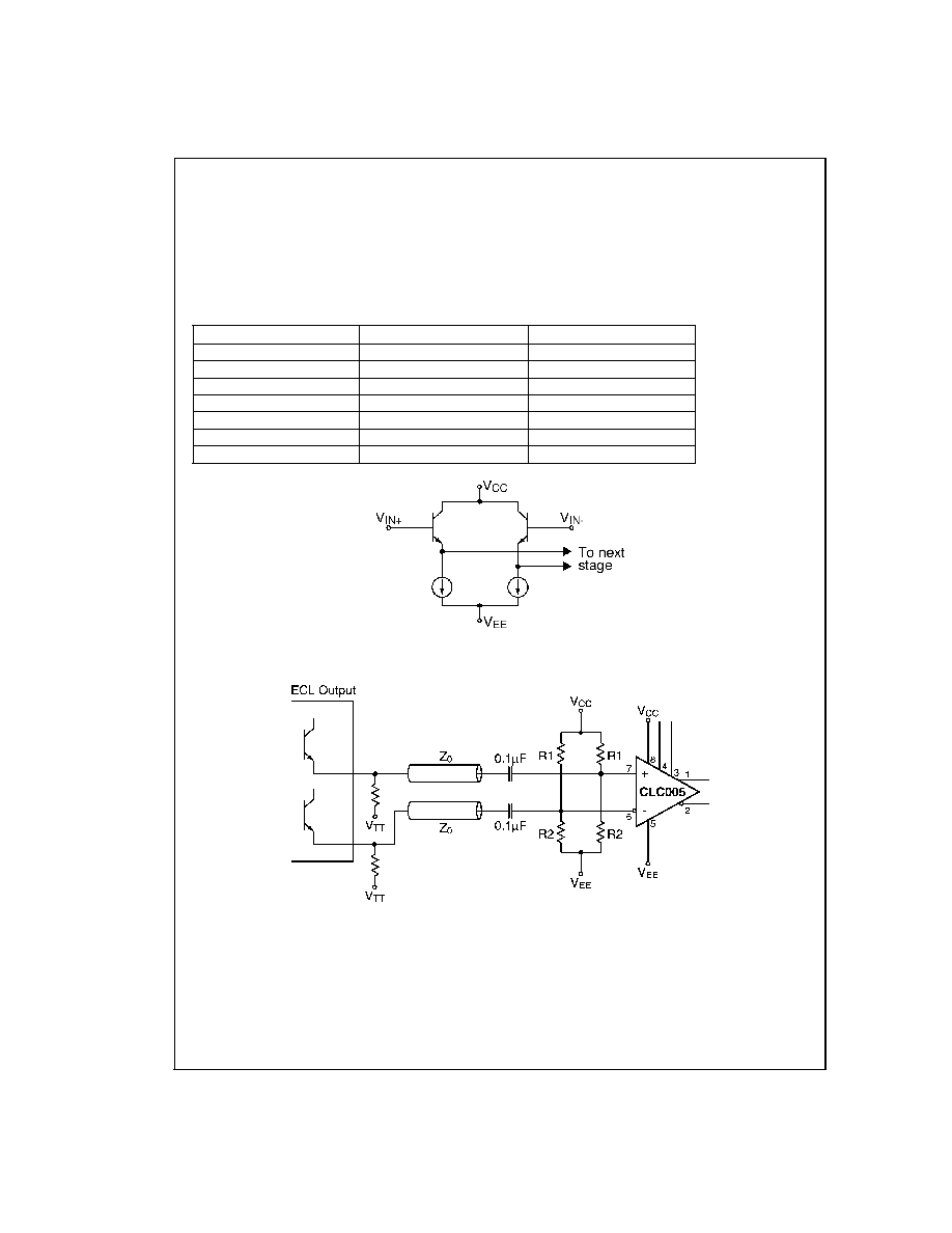
Load Type
Resistor to V
CC
(R1)
Resistor to V
EE
(R2)
ECL, 50
, 5V, V
T
=2V
82.5
124
ECL, 50
, 5.2V, V
T
=2V
80.6
133
ECL, 75
, 5V, V
T
=2V
124
187
ECL, 75
, 5.2V, V
T
=2V
121
196
800mV
P-P
, 50
, 5V, V
T
=1.6V
75.0
154
800mV
P-P
, 75
, 5V, V
T
=1.6V
110
232
800mV
P-P
, 2.2K
, 5V, V
T
=1.6V
3240
6810
DS100144-4
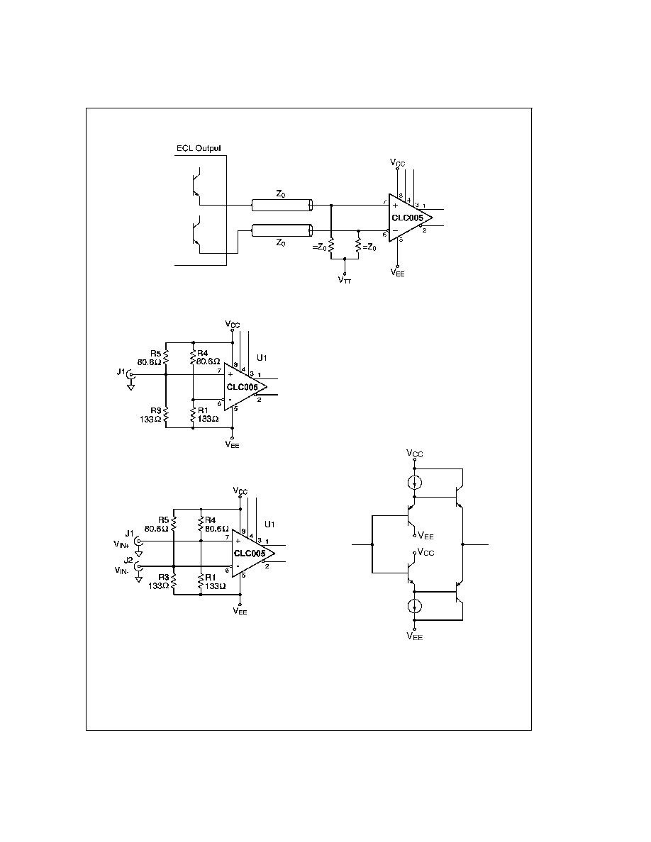
FIGURE 1. Input Stage
DS100144-5
FIGURE 2. AC Coupled Input
www.national.com
4
Operation
(Continued)
OUTPUT INTERFACING
The CLC005's class AB output stage,
Figure 6, requires no
standing current in the output transistors and therefore re-
quires no biasing or pull-down resistors. Advantages of this
arrangement are lower power dissipation and fewer external
components. The output may be either D.C. or A.C. coupled
to the load. A bandgap voltage reference sets output voltage
levels which are compatible with F100K and 10K ECL when
correctly terminated. The outputs do not have the same out-
put voltage temperature coefficient as 10K. Therefore, noise
margins will be reduced over the full temperature range
when driving 10K ECL. Noise margins will not be affected
when interfacing to F100K since F100K is fully voltage and
temperature compensated.
DS100144-6
FIGURE 3. DC Coupled Input
DS100144-7
FIGURE 4. Single Ended 50
ECL Input
DS100144-8
FIGURE 5. Differential 50
ECL Input
DS100144-9
FIGURE 6. Output Stage
5
www.national.com