 | ÐлекÑÑоннÑй компоненÑ: DP83907 | СкаÑаÑÑ:  PDF PDF  ZIP ZIP |
Äîêóìåíòàöèÿ è îïèñàíèÿ www.docs.chipfind.ru
TL F 12082
DP83907
ATLANTIC
II
PRELIMINARY
November 1995
DP83907 AT LANTIC
TM
II
General Description
The DP83907 Twisted-Pair Enhanced Coaxial Network In-
terface Controller is a CMOS VLSI device designed for easy
implementation of CSMA CD local area networks
Unique to the DP83907 is the integration of the entire bus
interface for PCAT ISA (Industry Standard Architecture) bus
based systems Hardware and software selectable options
allow the DP83907's bus interface to be configured in the
same manner as an NE2000 Architecture All bus drivers
and control logic are integrated to reduce board cost and
area
Supported
network
interfaces
include
10BASE5
or
10BASE2 Ethernet via an external transceiver connected to
its AUl port and Twisted-pair Ethernet
(10BASE-T) using
the on-board transceiver The DP83907 provides the Ether-
net Media Access Control (MAC) Encode-Decode (ENDEC)
with an AUl interface and 10BASE-T transceiver functions
in accordance with the lEEE 802 3 standards
The DP83907's integrated 10BASE-T transceiver fully com-
plies with the IEEE standard This functional block incorpo-
rates the receiver transmitter collision heartbeat loop-
back jabber and link integrity blocks as defined in the stan-
dard The transceiver when combined with equalization re-
sistors transmit receive filters and pulse transformers pro-
vides a complete physical interface from the DP83907's
ENDEC module and the twisted pair medium
(continued)
Features
Y
Controller and integrated bus interface solution for IEEE
802 3 10BASE5 10BASE2 and 10BASE-T
Y
Software compatible with industry standard Ethernet
Adapters Novell 's NE2000
Y
No external bus logic or drivers needed
Y
Supports jumpered or jumperless configuration
Y
Provides EEPROM interface for non-volatile storage of
configuration data
user-defined data and Ethernet
Physical Address
Y
Allows in-situ programming of EEPROM
Y
Integrated controller ENDEC and transceiver
Y
Full IEEE 802 3 compliant AUI interface
Y
Single 5V supply
10BASE-T TRANSCEIVER MODULE
Y
Integrates transceiver functionality
Y
Transmitter and receiver functions
Y
Collision detect heartbeat and jabber
Y
Selectable link integrity test or link disable
Y
Polarity Detection Correction
Y
Auto switch
Y
On chip filter
ENDEC MODULE
Y
10 Mbit s Manchester encoding decoding
Y
Squelch on receive and collision pairs
MAC CONTROLLER MODULE
Y
Software compatible with DP8390 DP83901 DP83902
Y
Efficient buffer management implementation
IN-CIRCUIT TEST
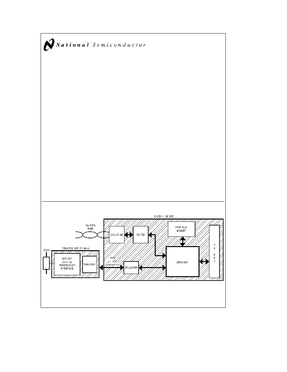
1 0 System Diagram
TL F 12082 1
TRI-STATE
is a registered trademark of National Semiconductor Corporation
AT LANTIC
TM
is a trademark of National Semiconductor Corporation
Ethernet
is a registered trademark of Xerox Corporation
NetWare
TM
is a trademark of Novell Incorporated
Novell
is a registered trademark of Novell Incorporated
C1995 National Semiconductor Corporation
RRD-B30M115 Printed in U S A

General Description
(Continued)
The integrated ENDEC module allows Manchester encod-
ing and decoding via a differential transceiver and phase
lock loop decoder at 10 Mbit sec Also included are a colli-
sion detect translator and diagnostic loopback capability
The ENDEC module interfaces directly to the transceiver
module and also provides a fully IEEE compliant AUI (At-
tachment Unit Interface) for connection to other media
transceivers
The Media Access Control function which is provided by the
Network Interface Control module (NIC) provides simple
and efficient packet transmission and reception control by
means of off-board memory which can be accessed through
an I O port
The DP83907 provides a comprehensive solution for
10BASE-T IEEE 802 3 networks Due to the inherent con-
straints of CMOS processing isolation is required at the AUI
differential signal interface for 10BASE5 and 10BASE2 ap-
plications
TabIe Of Contents
1 0 SYSTEM DIAGRAM
1 1 Connection Diagram
2 0 PIN DESCRIPTION
3 0 SIMPLIFIED APPLICATION DIAGRAM
4 0 FUNCTIONAL DESCRIPTION
4 1 Bus Interface Block
4 2 Power on RESET Operation
4 3 EEPROM OperatIon
4 4 Jumperless Operation Support
4 5 Ethernet Cable Configuratlon
4 6 Interrupt AND LED OperatIon
4 7 Boot PROM OperatIon
4 8 DP8390 Core (Network interface Controller)
4 9 Twisted Pair Interface Module
4 10 Encoder Decoder (ENDEC) Module
5 0 REGISTER DESCRIPTIONS
5 1 Configuration Registers
5 2 NIC Core Registers
5 3 DP8390 Core DMA Registers
6 0 OPERATION OF DP83907
6 1 Transmit Receive Packet Encapsulation Decapsula-
tion
6 2 Buffer Memory Access Control (DMA)
6 3 Packet Reception
6 4 Packet TransmissIon
6 5 Loopback DIagnostics
6 6 Memory Arbitration and Bus Operation
6 7 Functional Bus TimIng
7 0 IN-CIRCUIT TEST (ICT) DESCRIPTION
2
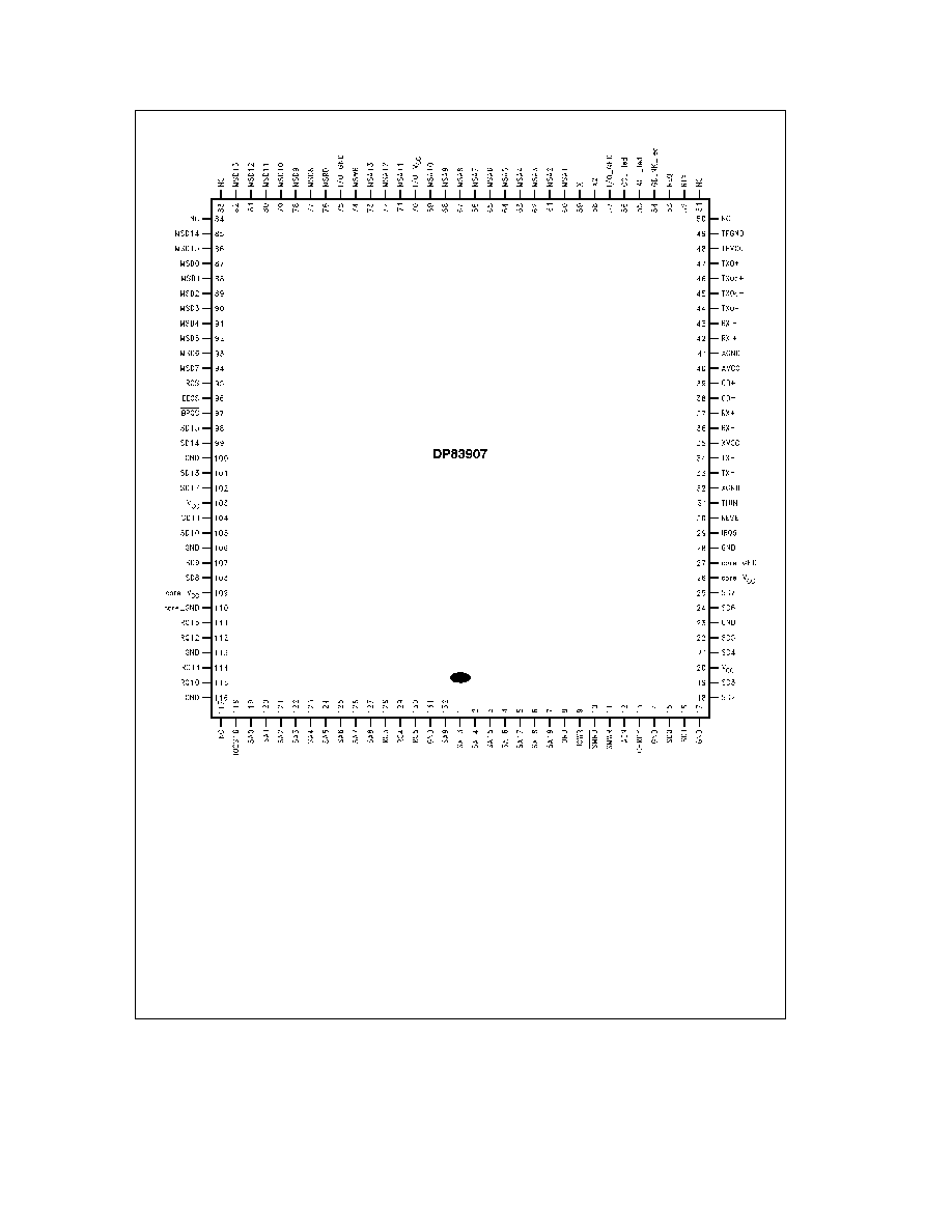
Connection Diagram
TL F 12082 2
Order Number DP83907VF
See NS Package Number VF132A
3
2 0 Pin Description
Pin No
Pin Name
Type
Description
ISA BUS INTERFACE PINS
119 127
SA0 SA9
I
LATCHED ADDRESS BUS
Low-order 10 bits of the system's latched 20-bit address
bus These bits are used to decode accesses to the DP83907's I O map
132
TTL
1 7
SA13 SA19
I
LATCHED ADDRESS BUS
7 bits of the system's latched 20-bit address bus that are
used to decode accesses to the DP83907's boot PROM
TTL
10 11
SMRD
I
BOOT PROM STROBES
These inputs are used to access the BOOT PROM
SMWR
TTL
15 16 18
SD0 SD7
I O
SYSTEM DATA BUS
16-bit system data bus Used to transfer data between the
system and the DP83907
19 21 22
SD8 SD15
3ST
24 25 98
99 101 102
104 105 107
108
118
IOCS16
O
16 BIT I O TRANSFER
This signal indicates that the DP83907 is responding to a 16-
bit I O access by driving 16 bits of data on the bus
OCH
9
IOWR
I
I O WRITE STROBE
Strobe from system to write to the DP83907's I O map
TTL
8
IORD
I
I O READ STROBE
Strobe from system to read from the DP83907's I O map
TTL
30
RESET
I
RESET
This signal is output by the system to reset all devices on the bus
TTL
13
CHRDY
O
CHANNEL READY
This signal is used to insert wait states into system accesses
OCH
12
AEN
I
DMA ACTIVE
This signal indicates that the systems DMA has control of the bus
TTL
29 111
IRQ3 4 5 9 10
O
INTERRUPT REQUEST
The operation of these outputs is determined by
Configuration Register A
112 114
11 12 15
3ST
115 128
129 130
Note
Driver Types are I
e
Input O
e
Output I O
e
Bi-directional Output OCH
e
Open Collector 3ST
e
TRI-STATE
Output TTL
e
TTL Compatible
AUI
e
Attachment Unit Interface TPI
e
Twisted Pair Interface LED
e
LED Drive MOS
e
CMOS Level Compatible XTAL
e
Crystal
4
2 0 Pin Description
(Continued)
Pin No
Pin Name
Type
Description
NETWORK INTERFACE PINS
44 47
TxOd
a
TXO
b
O
TWISTED PAIR TRANSMIT OUTPUTS
These high drive CMOS level outputs are
resistively combined external to the chip to produce a differential output signal with
TXO
a
TXOd
b
TPI
equalization to compensate for Intersymbol Interference (ISI) on the twisted pair medium
42 43
RXI
a
RXI
b
I
TWISTED PAIR RECEIVE INPUTS
These inputs feed a differential amplifier which passes
valid data to the ENDEC module
TPI
33 34
TX
b
O
AUI TRANSMIT OUTPUT
Differential driver which sends the encoded data to the
transceiver
TX
a
AUI
36 37
RX
b
I
AUI RECEIVE INPUT
Differential receive input pair from the transceiver
RX
a
AUI
38 39
CD
b
I
AUI COLLISION INPUT
Differential collision pair input from the transceiver
CD
a
AUI
55
ACT
led
O
ACTIVITY
An open-drain active low output It is asserted for approximately 50 ms
whenever the DP83907 transmits or receives data in either AUI or TPI modes
LED
56
COL
led
O
COLLISION
An open-drain active low output It is asserted for approximately 50 ms
whenever the DP83907 detects a collision in either either AUI or TPI modes
LED
54
GDLNK
led
O
GOOD LINK
An open-drain active low output This pin operates as an output to display link
integrity status if this function has not been disabled by the GDLNK bit in Configuratioin
LED
Register B
This output is off if the DP83907 is in AUI mode or if link testing is enabled and the link
integrity is bad (i e the twisted pair link has been broken)
This output is on if the DP83907 is in Twisted Pair interface (TPI) mode link integrity
checking is enabled and the link integrity is good (i e the twisted pair link has not been
broken) or if the link testing is disabled
53
REQ
I
EQUALIZATION RESISTOR
A resistor can be connected from this pin to GND or V
CC
to
change the equalization of the TP output
52
RTX
I
TRANSMIT LEVEL RESISTOR
A resistor can be connected from this pin to GND or V
CC
to
change the TP output amplitude level
59
X1 (OSCIN)
I
CRYSTAL ON EXTERNAL OSCILLATOR INPUT
XTAL
58
X2 (OSCOUT)
O
CRYSTAL FEEDBACK OUTPUT
Used in crystal connections only Should be left
unconnected when using an oscillator module
XTAL
31
THIN
O
THIN CABLE
This output is high if DP83907 is configured for thin cable It can be used to
enable the DC-DC converter required by the thin Ethernet configuration
DCDC
Note
Driver Types are I
e
Input O
e
Output I O
e
Bi-directional Output OCH
e
Open Collector 3ST
e
TRI-STATE Output TTL
e
TTL Compatible
AUI
e
Attachment Unit Interface TPI
e
Twisted Pair Interface LED
e
LED Drive MOS
e
CMOS Level Compatible XTAL
e
Crystal
5