 | –≠–ª–µ–∫—Ç—Ä–æ–Ω–Ω—ã–π –∫–æ–º–ø–æ–Ω–µ–Ω—Ç: DP8391A | –°–∫–∞—á–∞—Ç—å:  PDF PDF  ZIP ZIP |

TL F 9357
DP8391ANS32491A
SNI
Serial
Network
Interface
July 1993
DP8391A NS32491A SNI Serial Network Interface
General Description
The DP8391A Serial Network Interface (SNI) provides the
Manchester data encoding and decoding functions for
IEEE 802 3 Ethernet Cheapernet type local area networks
The SNI interfaces the DP8390 Network Interface Controller
(NIC) to the Ethernet transceiver cable When transmitting
the SNI converts non-return-to-zero (NRZ) data from the
controller and clock pulses into Manchester encoding and
sends the converted data differentially to the transceiver
The opposite process occurs on the receive path where a
digital phase-locked loop decodes 10 Mbit s signals with as
much as
g
18 ns of jitter
The DP8391A SNI is a functionally complete Manchester
encoder decoder including ECL like balanced driver and re-
ceivers on board crystal oscillator collision signal transla-
tor and a diagnostic loopback circuit
The SNI is part of a three chip set that implements the com-
plete IEEE compatible network node electronics as shown
below The other two chips are the DP8392 Coax Transceiv-
er Interface (CTI) and the DP8390 Network Interface Con-
troller (NIC)
Incorporated into the CTI are the transceiver collision and
jabber functions The Media Access Protocol and the buffer
management tasks are performed by the NIC There is an
isolation requirement on signal and power lines between the
CTI and the SNI This is usually accomplished by using a set
of miniature pulse transformers that come in a 16-pin plastic
DIP for signal lines Power isolation however is done by
using a DC to DC converter
Features
Y
Compatible with Ethernet II
IEEE 802 3
10Base5
10Base2 and 10Base-T
Y
10 Mb s Manchester encoding decoding with receive
clock recovery
Y
Patented digital phase locked loop (DPLL) decoder re-
quires no precision external components
Y
Decodes Manchester data with up to
g
18 ns of jitter
Y
Loopback capability for diagnostics
Y
Externally selectable half or full step modes of opera-
tion at transmit output
Y
Squelch circuits at the receive and collision inputs re-
ject noise
Y
High voltage protection at transceiver interface (16V)
Y
TTL MOS compatible controller interface
Y
Connects directly to the transceiver (AUI) cable
Table of Contents
1 0 System Diagram
2 0 Block Diagram
3 0 Functional Description
3 1
Oscillator
3 2
Encoder
3 3
Decoder
3 4
Collision Translator
3 5
Loopback
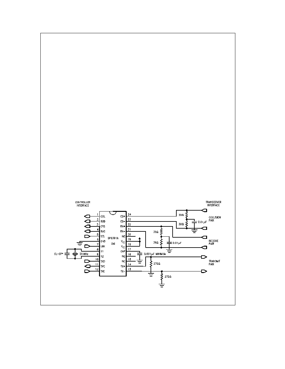
4 0 Connection Diagrams
5 0 Pin Descriptions
6 0 Absolute Maximum Ratings
7 0 Electrical Characteristics
8 0 Switching Characteristics
9 0 Timing and Load Diagrams
10 0 Physical Dimensions
1 0 System Diagram
IEEE 802 3 Compatible Ethernet Cheapernet Local Area Network Chip Set
TL F 9357 ≠ 1
C1995 National Semiconductor Corporation
RRD-B30M105 Printed in U S A

2 0 Block Diagram
TL F 9357 ≠ 2
FIGURE 1
3 0 Functional Description
The SNI consists of five main logical blocks
a) the oscillator
generates the 10 MHz transmit clock sig-
nal for system timing
b) the Manchester encoder and differential output driver
accepts NRZ data from the controller performs Man-
chester encoding and transmits it differentially to the
transceiver
c) the Manchester decoder
receives Manchester data
from the transceiver converts it to NRZ data and clock
pulses and sends them to the controller
d) the collision translator
indicates to the controller the
presence of a valid 10 MHz signal at its input
e) the loopback circuitry
when asserted switches encod-
ed data instead of receive input signals to the digital
phase-locked loop
3 1 OSCILLATOR
The oscillator is controlled by a 20 MHz parallel resonant
crystal connected between X1 and X2 or by an external
clock on X1 The 20 MHz output of the oscillator is divided
by 2 to generate the 10 MHz transmit clock for the control-
ler The oscillator also provides internal clock signals to the
encoding and decoding circuits
Crystal Specification
Resonant frequency
20 MHz
Tolerance
g
0 001% at 25 C
Stability
g
0 005% 0 ≠ 70 C
Type
AT-Cut
Circuit
Parallel Resonance
The 20 MHz crystal connection to the SNI requires special
care The IEEE 802 3 standard requires a 0 01% absolute
accuracy on the transmitted signal frequency Stray capaci-
tance can shift the crystal's frequency out of range causing
the transmitted frequency to exceed its 0 01% tolerance
The frequency marked on the crystal is usually measured
with a fixed shunt capacitance (C
L
) that is specified in the
crystal's data sheet This capacitance for 20 MHz crystals is
typically 20 pF The capacitance between the X1 and X2
pins of the SNI of the PC board traces and the plated
through holes plus any stray capacitance such as the sock-
et capacitance if one is used should be estimated or mea-
sured Once the total sum of these capacitances is deter-
mined the value of additional external shunt capacitance
required can be calculated This capacitor can be a fixed
5% tolerance component The frequency accuracy should
be measured during the design phase at the transmit clock
pin (TXC) for a given pc layout
Figure 2 shows the crystal
connection
TL F 9357 ≠ 3
CL
e
Load capacitance specified by the crystal's manufacturer
CP
e
Total parasitic capacitance including
a) SNI input capacitance between X1 and X2 (typically 5 pF)
b) PC board traces plated through holes socket capacitances
Note 1
When using a Viking (San Jose) VXB49N5 crystal the external ca-
pacitor is not required as the C
L
of the crystal matches the input
capacitance of the DP8391A
FIGURE 2 Crystal Connection
3 2 MANCHESTER ENCODER AND DIFFERENTIAL
DRIVER
The encoder combines clock and data information for the
transceiver Data encoding and transmission begins with the
transmit enable input (TXE) going high As long as TXE re-
2
3 0 Functional Description
(Continued)
mains high transmit data (TXD) is encoded out to the trans-
mit-driver pair (TX
g
) The transmit enable and transmit data
inputs must meet the setup and hold time requirements with
respect to the rising edge of transmit clock Transmission
ends with the transmit enable input going low The last tran-
sition is always positive at the transmit output pair It will
occur at the center of the bit cell if the last bit is one or at
the boundary of the bit cell if the last bit is zero
The differential line driver provides ECL like signals to the
transceiver with typically 5 ns rise and fall times It can drive
up to 50 meters of twisted pair AUI Ethernet transceiver
cable These outputs are source followers which need ex-
ternal 270X pulldown resistors to ground Two different
modes full-step or half-step can be selected with SEL in-
put With SEL low transmit
a
is positive with respect to
transmit
b
in the idle state With SEL high transmit
a
and
transmit
b
are equal in the idle state providing zero differ-
ential voltage to operate with transformer coupled loads
Figures 4 5 and 6 illustrate the transmit timing
3 3 MANCHESTER DECODER
The decoder consists of a differential input circuitry and a
digital phase-locked loop to separate Manchester encoded
data stream into clock signals and NRZ data The differen-
tial input should be externally terminated if the standard
78X transceiver drop cable is used Two 39X resistors con-
nected in series and one optional common mode bypass
capacitor would accomplish this A squelch circuit at the
input rejects signals with pulse widths less than 5 ns (nega-
tive going) or with levels less than
b
175 mV Signals more
negative than
b
300 mV and with a duration greater than
30 ns are always decoded This prevents noise at the input
from falsely triggering the decoder in the absence of a valid
signal Once the input exceeds the squelch requirements
carrier sense (CRS) is asserted Receive data (RXD) and
receive clock (RXC) become available typically within 6 bit
times At this point the digital phase-locked loop has locked
to the incoming signal The DP8391A decodes a data frame
with up to
g
18 ns of jitter correctly
The decoder detects the end of a frame when the normal
mid-bit transition on the differential input ceases Within one
and a half bit times after the last bit carrier sense is de-as-
serted Receive clock stays active for five more bit times
before it goes low and remains low until the next frame
Figures 7 8 and 9 illustrate the receive timing
3 4 COLLISION TRANSLATOR
The Ethernet transceiver detects collisions on the coax ca-
ble and generates a 10 MHz signal on the transceiver cable
The SNI's collision translator asserts the collision detect
output (COL) to the DP8390 controller when a 10 MHz sig-
nal is present at the collision inputs The controller uses this
signal to back off transmission and recycle itself The colli-
sion detect output is de-asserted within 350 ns after the 10
MHz input signal disappears
The collision differential inputs (
a
and
b
) should be termi-
nated in exactly the same way as the receive inputs The
collision input also has a squelch circuit that rejects signals
with pulse widths less than 5 ns (negative going) or with
levels less than
b
175 mV
Figure 10 illustrates the collision
timing
3 5 LOOPBACK FUNCTIONS
Logic high at loopback input (LBK) causes the SNI to route
serial data from the transmit data input through its encoder
returning it through the phase-locked-loop decoder to re-
ceive data output In loopback mode the transmit driver is in
idle state and the receive and collision input circuitries are
disabled
4 0 Connection Diagram
Top View
Refer to the Oscillator section
TL F 9357 ≠ 4
FIGURE 3a
Order Number DP8391AN
See NS Package Number N24C
3

PCC Connection Diagram
TL F 9357 ≠ 5
Refer to the Oscillator section
FIGURE 3b
Order Number DP8391AV
NS Package Number V28A
4
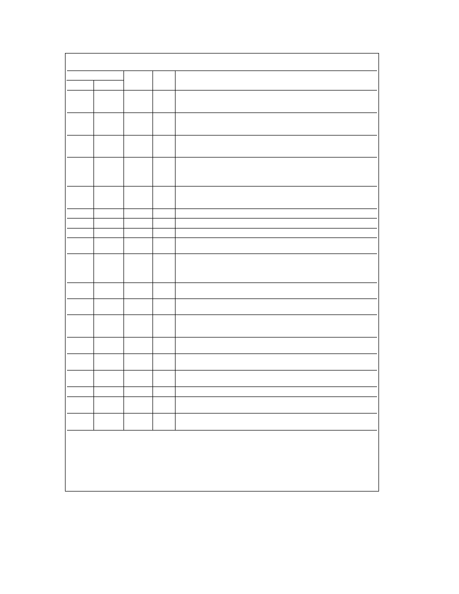
5 0 Pin Descriptions
Pin No
Name
I O
Description
(DIP)
(PCC)
1
1
COL
O
Collision Detect Output
A TTL MOS level active high output A 10 MHz
(
a
25% ≠ 15%) signal at the collision input will produce a logic high at COL
output When no signal is present at the collision input COL output will go low
2
2
RXD
O
Receive Data Output
A TTL MOS level signal This is the NRZ data output
from the digital phase-locked loop This signal should be sampled by the
controller at the rising edge of receive clock
3
3
CRS
O
Carrier Sense
A TTL MOS level active high signal It is asserted when valid
data from the transceiver is present at the receive input It is de-asserted one
and a half bit times after the last bit at receive input
4
4
RXC
O
Receive Clock
A TTL MOS level recovered clock When the phase-locked loop
locks to a valid incoming signal a 10 MHz clock signal is activated on this output
This output remains low during idle (5 bit times after activity ceases at receive
input)
5
5
SEL
I
Mode Select
A TTL level input When high transmit
a
and transmit
b
outputs
are at the same voltage in idle state providing a ``zero'' differential When low
transmit
a
is positive with respect to transmit
b
in idle state
6
6 ≠ 9
GND
Negative Supply Pins
7
10
LBK
I
Loopback
A TTL level active high on this input enables the loopback mode
8
11
X1
I
Crystal or External Frequency Source Input (TTL)
9
12
X2
O
Crystal Feedback Output
This output is used in the crystal connection only It
must be left open when driving X1 with an external frequency source
10
13
TXD
I
Transmit Data
A TTL level input This signal is sampled by the SNI at the rising
edge of transmit clock when transmit enable input is high The SNI combines
transmit data and transmit clock signals into a Manchester encoded bit stream
and sends it differentially to the transceiver
11
14
TXC
O
Transmit Clock
A TTL MOS level 10 MHz clock signal derived from the 20
MHz oscillator This clock signal is always active
12
15
TXE
I
Transmit Enable
A TTL level active high data encoder enable input This signal
is also sampled by the SNI at the rising edge of transmit clock
13
16
TX
b
O
Transmit Output
Differential line driver which sends the encoded data to the
transceiver These outputs are source followers and require 270X pulldown
14
17
TX
a
resistors to GND
15
18
NC
No Connection
16
17
19
CAP
O
Bypass Capacitor
A ceramic capacitor (greater than 0 001 mF) must be
connected from this pin to GND
18
20 ≠ 23
VCC
Positive Supply Pins
A 0 1 mF ceramic decoupling capacitor must be
connected across VCC and GND as close to the device as possible
19
20
24
NC
No Connection
21
25
RX
b
I
Receive Input
Differential receive input pair from the transceiver
22
26
RX
a
23
27
CD
b
I
Collision Input
Differential collision input pair from the transceiver
24
28
CD
a
5