 | –≠–ª–µ–∫—Ç—Ä–æ–Ω–Ω—ã–π –∫–æ–º–ø–æ–Ω–µ–Ω—Ç: DS14C202 | –°–∫–∞—á–∞—Ç—å:  PDF PDF  ZIP ZIP |
DS14C202
Low Power +5V Powered EIA/TIA-232 Dual
Driver/Receiver
General Description
The DS14C202 is a low power dual driver/receiver featuring
an onboard DC to DC converter. This eliminates the need for
±
12V power supplies and requires only a +5V power supply.
Only four 0.1 µF capacitors are needed for the DC to DC
converter. The drivers maintain greater than
±
5V output sig-
nal levels at data rates in excess of 128 kbits/sec when
loaded in accordance with the EIA/TIA-232-E specification.
I
CC
is specified at 15 mA maximum, making the device ideal
for battery and power conscious applications. The drivers'
slew rate is set internally, eliminating the need for external
slew rate capacitors. The device is designed to interface
data terminal equipment (DTE) with data circuit-terminating
equipment (DCE). The driver inputs and receiver outputs are
TTL and CMOS compatible. DS14C202 driver outputs and
receiver inputs meet EIA/TIA-232-E and ITU-T V.28 stan-
dards. This device is an enhanced version of the DS14C232
that requires smaller external capacitors (0.1 µF) and sup-
ports higher data rates of up to 128 kbit/sec.
Features
n
Uses only four small 0.1 µF capacitors for DC to DC
converter
n
Operates over 128 kbit/sec
n
Pin compatible with MAX202, MAX232A and others
n
Single +5V power supply
n
Low power
n
DS14C202 meets EIA/TIA-232-E and ITU-T V.28
standards
n
CMOS technology
n
Package efficiency -- 2 drivers and 2 receivers
n
Available in Plastic DIP and Narrow SOIC packages
n
Extended temperature range: -40∞C to +85∞C
n
ESD
6.0 kV HBM
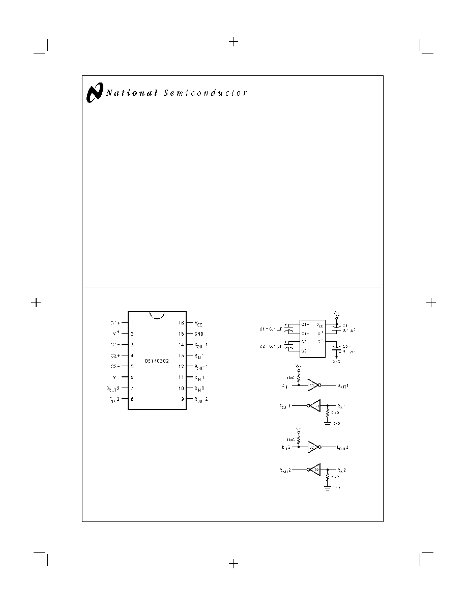
Connection Diagram
Functional Diagram
DS012622-1
Order Number DS14C202TN
or DS14C202TM
See NS Package Number N16A or M16A
DS012622-2
ADVANCE INFORMATION
June 1998
DS14C202
Low
Power
+5V
Powered
EIA/TIA-232
Dual
Driver/Receiver
DS14C202
© 1998 National Semiconductor Corporation
DS012622
www.national.com
1
PrintDate=1998/06/22 PrintTime=10:23:03 42589 ds012622 Rev. No. 0
cmserv
Proof
1
Absolute Maximum Ratings
(Note 1)
If Military/Aerospace specified devices are required,
please contact the National Semiconductor Sales Office/
Distributors for availability and specifications.
Supply Voltage (V
CC
)
-0.3V to 6V
Supply Voltage (V
+
)
(V
CC
- 0.3V) to +14V
Supply Voltage (V
-
)
+0.3V to -14V
Short Circuit Duration, D
OUT
Continuous
Driver Input Voltage
-0.3V to (V
CC
+ 0.3V)
Driver Output Voltage
(V
+
+ 0.3V) to (V
-
- 0.3V)
Receiver Input Voltage
±
25V
Receiver Output Voltage
-0.3V to (V
CC
+ 0.3V)
ESD Rating
(HBM, 1.5 k
, 100 pF)
6.0 kV
Junction Temperature
+150∞C
Maximum Package Power Dissipation
@
25∞C (Note 6)
N Package
TBD
M Package
TBD
Storage Temperature Range
-65∞C to +150∞C
Lead Temperature
(Soldering, 4 sec.)
+260∞C
Recommended Operating
Conditions
Min
Max
Units
Supply Voltage, (V
CC
)
4.5
5.5
V
Operating Free Air Temp. (T
A
)
DS14C202T
-40
+85
∞C
Electrical Characteristics
(Notes 2, 5)
Over recommended operating conditions, unless otherwise specified.
Symbol
Parameter
Conditions
Min
Typ
Max
Units
DEVICE CHARACTERISTICS
V
+
Positive Power Supply
R
L
= 3 k
, C1≠C4 = 0.1 µF, D
IN
= 0.8V
9.0
V
V
-
Negative Power Supply
R
L
= 3 k
, C1≠C4 = 0.1 µF, D
IN
= 2.0V
-8.5
V
I
CC
V
CC
Supply Current
No Load
15
mA
DRIVER CHARACTERISTICS
V
IH
High Level Input Voltage
2.0
V
CC
V
V
IL
Low Level Input Voltage
GND
0.8
V
I
IH
High Level Input Current
V
IN
2.0V
-30
+30
µA
I
IL
Low Level Input Current
V
IN
0.8V
-30
+30
µA
V
OH
High Level Output Voltage
R
L
= 3 k
5.0
8.0
V
V
OL
Low Level Output Voltage
R
L
= 3 k
-7.0
-5.0
V
I
OS
+
Output High Short Circuit Current
V
OUT
= 0V, V
IN
= 0.8V
(Note 3)
-5.0
-15
-30
mA
I
OS
-
Output Low Short Circuit Current
V
OUT
= 0V, V
IN
= 2.0V
5.0
11
30
mA
R
O
Output Resistance
-2V
V
OUT
+2V, V
CC
= 0V = GND or Open
300
RECEIVER CHARACTERISTICS
V
TH
Input High Threshold Voltage
1.7
2.4
V
V
TL
Input Low Threshold Voltage
0.8
1.5
V
V
HY
Hysteresis
0.2
0.4
1.0
V
R
IN
Input Resistance
-15V
V
IN
+15V
3.0
4.7
7.0
k
I
IN
Input Current
V
IN
= +15V
+2.14
+3.5
+5.0
mA
V
IN
= +3V
+0.43
+0.6
+1.0
mA
V
IN
= -3V
-0.43
-0.6
-1.0
mA
V
IN
= -15V
-2.14
-3.5
-5.0
mA
V
OH
High Level Output Voltage
V
IN
= -3V, I
OH
= -3.2 mA
3.5
4.5
V
V
IN
= -3V, I
OH
= -20 µA
4.0
4.9
V
V
OL
Low Level Output Voltage
V
IN
= +3V, I
OL
= +3.2 mA
0.15
0.4
V
PrintDate=1998/06/22 PrintTime=10:23:03 42589 ds012622 Rev. No. 0
cmserv
Proof
2
www.national.com
2

Switching Characteristics
(Note 5)
Over recommended operating conditions, unless otherwise specified.
Symbol
Parameter
Conditions
Min
Typ
Max
Units
DRIVER CHARACTERISTICS
t
PLH
Propagation Delay Low to High
R
L
= 3 k
C
L
= 50 pF
(
Figure 1)
1.0
4.0
µs
t
PHL
Propagation Delay High to Low
1.0
4.0
µs
t
SK
Skew |t
PLH
- t
PHL
|
0.1
1.0
µs
SR1
Output Slew Rate
R
L
= 3 k
to 7 k
, C
L
= 50 pF
(Note 7)
4.0
10
30
V/µs
SR2
Output Slew Rate
R
L
= 3 k
to 7 k
, C
L
= 2500 pF
4.0
10
30
V/µs
RECEIVER CHARACTERISTICS
t
PLH
Propagation Delay Low to High
Input Pulse Width
>
10 µs
C
L
= 50 pF
(
Figure 2)
2.0
µs
t
PHL
Propagation Delay High to Low
2.0
µs
t
SK
Skew |t
PLH
- t
PHL
|
300
ns
t
r
Output Rise Time
15
ns
t
f
Output Fall Time
15
ns
DATA RATES
f
MAX
Maximum Data Rate
R
L
= 3 k
to 7 k
, C
L
= 50 pF to 1000 pF (Note 8)
128
TBD
kbps
Note 1: Absolute Maximum Ratings are those values beyond which the safety of the device cannot be guaranteed. They are not meant to imply that the devices
should be operated at these limits. The table of Electrical Characteristics specify conditions for device operation.
Note 2: Current into device pins is defined as positive. Current out of device pins is defined as negative. All voltages are referenced to ground unless otherwise speci-
fied. For current, minimum and maximum values are specified as an absolute value and the sign is used to indicate direction. For voltage logic levels, the more posi-
tive value is designated as maximum. For example, if -6V is a maximum, the typical value of -6.8V is more negative.
Note 3: I
OS
+
and I
OS
-
values are for one output at a time.
Note 4: Receiver AC input waveform for test purposes: t
r
= t
f
= 160 ns (10% to 90%), V
IH
= 3V, V
IL
= -3V, f = 64 kHz, 50% duty cycle. Driver AC input waveform
for test purposes: t
r
= t
f
= 10 ns (10% to 90%), V
IH
= 3V, V
IL
= 0V, f = 64 kHz, 50% duty cycle.
Note 5: All typicals are given for V
CC
= 5.0V, +25∞C.
Note 6: Ratings apply to ambient temperature at +25∞C. Above this temperature derate: N Package TBD and M Package TBD.
Note 7: Slew rate is defined as
V/
t, measured between
±
3V level.
Note 8: f
MAX
criteria is either 60%≠40% duty cycle or a waveform that is
1
/
3
rise,
1
/
3
fall,
1
/
3
logic level (driver
±
5V and receiver 3.5V/0.4V).
Parameter Measurement Information
DS012622-3
DS012622-4
FIGURE 1. Driver Load Circuit and Switching Waveform (Note 4)
DS012622-5
DS012622-6
t
r
and t
f
measured between 20% and 80% of the waveform.
FIGURE 2. Receiver Load Circuit and Switching Waveform (Note 4)
3
www.national.com
PrintDate=1998/06/22 PrintTime=10:23:03 42589 ds012622 Rev. No. 0
cmserv
Proof
3
Pin Descriptions
V
CC
(Pin 16)
Power supply pin for the device, +5V (
±
10%).
V
+
(Pin 2)
Positive supply for EIA/TIA-232-E drivers. Recommended
external capacitor: C4 = 0.1 µF (
6.3V). Capacitor value
should not be less than 0.1 µF. This supply is not intended to
be loaded externally. (Note 9)
V
-
(Pin 6)
Negative supply for EIA/TIA-232-E drivers. Recommended
external capacitor: C3 = 0.1 µF (
16V). Capacitor value
should not be less than 0.1 µF. This supply is not intended to
be loaded externally. (Note 9)
C1+, C1- (Pins 1, 3)
External capacitor connection pins. Recommended capaci-
tor: C1 = 0.1 µF (
6.3V). Capacitor value should not be less
than 0.1 µF. (Note 9)
C2+, C2- (Pins 4, 5)
External capacitor connection pins. Recommended capaci-
tor: C2 = 0.1 µF (
16V). Capacitor value should not be less
than 0.1 µF. (Note 9)
D
IN
1, D
IN
2 (Pins 11, 10)
Driver input pins are TTL/CMOS compatible. Inputs of un-
used drivers may be left open, an internal active pull-up re-
sistor (500 k
minimum, typically 1 M
) pulls input HIGH.
Output will be LOW for input pins.
D
OUT
1, D
OUT
2 (Pins 14, 7)
Driver output pins conform to EIA/TIA-232-E levels.
R
IN
1, R
IN
2 (Pins 13, 8)
Receiver input pins accept EIA/TIA-232-E input voltages
(
±
25V). Receivers feature guaranteed hysteresis of 200 mV.
Unused receiver input pins may be left open. Internal input
resistor (5 k
) pulls input LOW, providing a fail-safe HIGH
output.
R
OUT
1, R
OUT
2 (Pins 12, 9)
Receiver output pins are TTL/CMOS compatible. Receiver
output HIGH voltage is specified for both CMOS and TTL
load conditions.
GND (Pin 15)
Ground Pin.
Note 9: All capacitor values have tolerances of less than
±
20%.
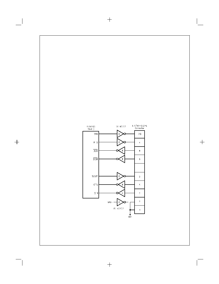
Typical Application Information
Application of DS14C202 and INS8250
DS012622-7
PrintDate=1998/06/22 PrintTime=10:23:03 42589 ds012622 Rev. No. 0
cmserv
Proof
4
Book
Extract
End
www.national.com
4

Typical Connection Diagram
DS012622-8
5
www.national.com
PrintDate=1998/06/22 PrintTime=10:23:03 42589 ds012622 Rev. No. 0
cmserv
Proof
5
Book
Extract
End