 | –≠–ª–µ–∫—Ç—Ä–æ–Ω–Ω—ã–π –∫–æ–º–ø–æ–Ω–µ–Ω—Ç: DS90C031B | –°–∫–∞—á–∞—Ç—å:  PDF PDF  ZIP ZIP |
DS90C031B
LVDS Quad CMOS Differential Line Driver
General Description
The DS90C031B is a quad CMOS differential line driver de-
signed for applications requiring ultra low power dissipation
and high data rates. The device is designed to support data
rates in excess of 155.5 Mbps (77.7 MHz) utilizing Low Volt-
age Differential Signaling (LVDS) technology.
The DS90C031B accepts TTL/CMOS input levels and trans-
lates them to low voltage (350 mV) differential output sig-
nals. In addition the driver supports a TRI-STATE
Æ
function
that may be used to disable the output stage, disabling the
load current, and thus dropping the device to an ultra low idle
power state of 11 mW typical.
In addition, the DS90C031B provides power-off high imped-
ance LVDS outputs. This feature assures minimal loading ef-
fect on the LVDS bus lines when V
CC
is not present.
The DS90C031B and companion line receiver (DS90C032B)
provide a new alternative to high power pseudo-ECL devices
for high speed point-to-point interface applications.
Features
n
>
155.5 Mbps (77.7 MHz) switching rates
n
High impedance LVDS outputs with power-off
n
±
350 mV differential signaling
n
Ultra low power dissipation
n
400 ps maximum differential skew (5V, 25∞C)
n
3.5 ns maximum propagation delay
n
Industrial operating temperature range
n
Pin compatible with DS26C31, MB571 (PECL) and
41LG (PECL)
n
Conforms to ANSI/TIA/EIA-644 LVDS standard
n
Offered in narrow and wide body SOIC package
n
Fail-safe logic for floating inputs
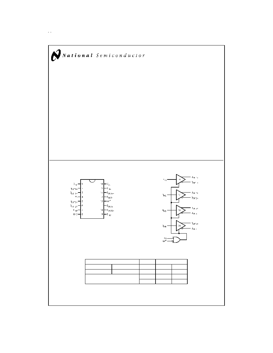
Connection Diagram
Functional Diagram
Driver Truth Table
Enables
Input
Outputs
EN
EN*
D
IN
D
OUT+
D
OUT-
L
H
X
Z
Z
All other combinations
L
L
H
of ENABLE inputs
H
H
L
TRI-STATE
Æ
is a registered trademark of National Semiconductor Corporation.
Dual-In-Line
DS100989-1
Order Number
DS90C031BTM,
or DS90C031BTWM
See NS Package Number
M16A or M16B
DS100989-2
March 1999
DS90C031B
L
VDS
Quad
CMOS
Differential
Line
Driver
© 1999 National Semiconductor Corporation
DS100989
www.national.com
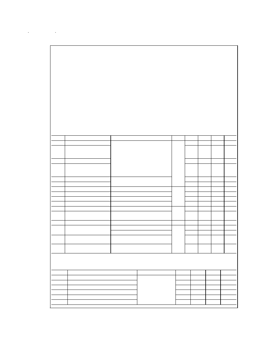
Absolute Maximum Ratings
(Note 1)
If Military/Aerospace specified devices are required,
please contact the National Semiconductor Sales Office/
Distributors for availability and specifications.
Supply Voltage (V
CC
)
-0.3V to +6V
Input Voltage (D
IN
)
-0.3V to (V
CC
+ 0.3V)
Enable Input Voltage (EN, EN*)
-0.3V to (V
CC
+ 0.3V)
Output Voltage (D
OUT+
, D
OUT-
)
-0.3V to +5.8V
Short Circuit Duration
(D
OUT+
, D
OUT-
)
Continuous
Maximum Package Power Dissipation
@
+25∞C
M Package
1068 mW
WM Package
1562 mW
Derate M Package
8.5 mW/∞C above +25∞C
Derate WM Package
12.5 mW/∞C above +25∞C
Storage Temperature Range
-65∞C to +150∞C
Lead Temperature Range
Soldering (4 sec.)
+260∞C
Maximum Junction
Temperature
+150∞C
ESD Rating (Note 7)
(HBM, 1.5 k
, 100 pF)
2kV
(EIAJ, 0
, 200 pF)
250V
Recommended Operating
Conditions
Min
Typ
Max
Units
Supply Voltage (V
CC
)
+4.5
+5.0
+5.5
V
Operating Free Air Temperature (T
A
)
DS90C031BT
-40
+25
+85
∞C
Electrical Characteristics
Over supply voltage and operating temperature ranges, unless otherwise specified. (Notes 2, 3)
Symbol
Parameter
Conditions
Pin
Min
Typ
Max
Units
V
OD1
Differential Output Voltage
R
L
= 100
(
Figure 1)
D
OUT-
,
D
OUT+
250
345
450
mV
V
OD1
Change in Magnitude of
V
OD1
for Complementary
Output States
4
35
|mV|
V
OS
Offset Voltage
1.10
1.25
1.35
V
V
OS
Change in Magnitude of
V
OS
for Complementary
Output States
5
25
|mV|
V
OH
Output Voltage High
R
L
= 100
1.41
1.60
V
V
OL
Output Voltage Low
0.90
1.07
V
V
IH
Input Voltage High
D
IN
,
EN,
EN*
2.0
V
CC
V
V
IL
Input Voltage Low
GND
0.8
V
I
I
Input Current
V
IN
= V
CC
, GND, 2.5V or 0.4V
-10
±
1
+10
µA
V
CL
Input Clamp Voltage
I
CL
= -18 mA
-1.5
-0.8
V
I
OS
Output Short Circuit Current
V
OUT
= 0V (Note 8)
D
OUT-
,
D
OUT+
-3.5
-5.0
mA
I
OZ
Output TRI-STATE Current
EN = 0.8V and EN* = 2.0V,
V
OUT
= 0V or V
CC
-10
±
1
+10
µA
I
OFF
Power - Off Leakage
V
O
= 0V or 2.4V, V
CC
= 0V or Open
-10
±
1
+10
µA
I
CC
No Load Supply Current
Drivers Enabled
D
IN
= V
CC
or GND
V
CC
1.7
3.0
mA
D
IN
= 2.5V or 0.4V
4.0
6.5
mA
I
CCL
Loaded Supply Current
Drivers Enabled
R
L
= 100
(all channels)
V
IN
= V
CC
or GND (all inputs)
15.4
21.0
mA
I
CCZ
No Load Supply Current
Drivers Disabled
D
IN
= V
CC
or GND
EN = GND, EN* = V
CC
2.2
4.0
mA
Switching Characteristics
V
CC
= +5.0V, T
A
= +25∞C (Notes 3, 6, 9)
Symbol
Parameter
Conditions
Min
Typ
Max
Units
t
PHLD
Differential Propagation Delay High to Low
R
L
= 100
, C
L
= 5 pF
(
Figure 2 and Figure 3)
1.0
2.0
3.0
ns
t
PLHD
Differential Propagation Delay Low to High
1.0
2.1
3.0
ns
t
SKD
Differential Skew |t
PHLD
≠ t
PLHD
|
0
80
400
ps
t
SK1
Channel-to-Channel Skew (Note 4)
0
300
600
ps
t
TLH
Rise Time
0.35
1.5
ns
t
THL
Fall Time
0.35
1.5
ns
www.national.com
2
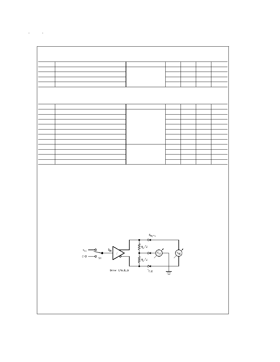
Switching Characteristics
(Continued)
V
CC
= +5.0V, T
A
= +25∞C (Notes 3, 6, 9)
Symbol
Parameter
Conditions
Min
Typ
Max
Units
t
PHZ
Disable Time High to Z
R
L
= 100
, C
L
= 5 pF
(
Figure 4 and Figure 5)
2.5
10
ns
t
PLZ
Disable Time Low to Z
2.5
10
ns
t
PZH
Enable Time Z to High
2.5
10
ns
t
PZL
Enable Time Z to Low
2.5
10
ns
Switching Characteristics
V
CC
= +5.0V
±
10%, T
A
= -40∞C to +85∞C (Notes 3, 6, 9)
Symbol
Parameter
Conditions
Min
Typ
Max
Units
t
PHLD
Differential Propagation Delay High to Low
R
L
= 100
, C
L
= 5 pF
(
Figure 2 and Figure 3)
0.5
2.0
3.5
ns
t
PLHD
Differential Propagation Delay Low to High
0.5
2.1
3.5
ns
t
SKD
Differential Skew |t
PHLD
≠ t
PLHD
|
0
80
900
ps
t
SK1
Channel-to-Channel Skew (Note 4)
0
0.3
1.0
ns
t
SK2
Chip to Chip Skew (Note 5)
3.0
ns
t
TLH
Rise Time
0.35
2.0
ns
t
THL
Fall Time
0.35
2.0
ns
t
PHZ
Disable Time High to Z
R
L
= 100
, C
L
= 5 pF
(
Figure 4 and Figure 5)
2.5
15
ns
t
PLZ
Disable Time Low to Z
2.5
15
ns
t
PZH
Enable Time Z to High
2.5
15
ns
t
PZL
Enable Time Z to Low
2.5
15
ns
Note 1: "Absolute Maximum Ratings" are those values beyond which the safety of the device cannot be guaranteed. They are not meant to imply that the devices
should be operated at these limits. The table of "Electrical Characteristics" specifies conditions of device operation.
Note 2: Current into device pins is defined as positive. Current out of device pins is defined as negative. All voltages are referenced to ground except: V
OD1
and
V
OD1
.
Note 3: All typicals are given for: V
CC
= +5.0V, T
A
= +25∞C.
Note 4: Channel-to-Channel Skew is defined as the difference between the propagation delay of the channel and the other channels in the same chip with an event
on the inputs.
Note 5: Chip to Chip Skew is defined as the difference between the minimum and maximum specified differential propagation delays.
Note 6: Generator waveform for all tests unless otherwise specified: f = 1 MHz, Z
O
= 50
, t
r
6 ns, and t
f
6 ns.
Note 7: ESD Ratings:
HBM (1.5 k
, 100 pF)
2kV
EIAJ (0
, 200 pF)
250V
Note 8: Output short circuit current (I
OS
) is specified as magnitude only, minus sign indicates direction only.
Note 9: C
L
includes probe and jig capacitance.
Parameter Measurement Information
DS100989-3
FIGURE 1. Driver V
OD
and V
OS
Test Circuit
www.national.com
3

Parameter Measurement Information
(Continued)
DS100989-4
FIGURE 2. Driver Propagation Delay and Transition Time Test Circuit
DS100989-5
FIGURE 3. Driver Propagation Delay and Transition Time Waveforms
DS100989-6
FIGURE 4. Driver TRI-STATE Delay Test Circuit
www.national.com
4
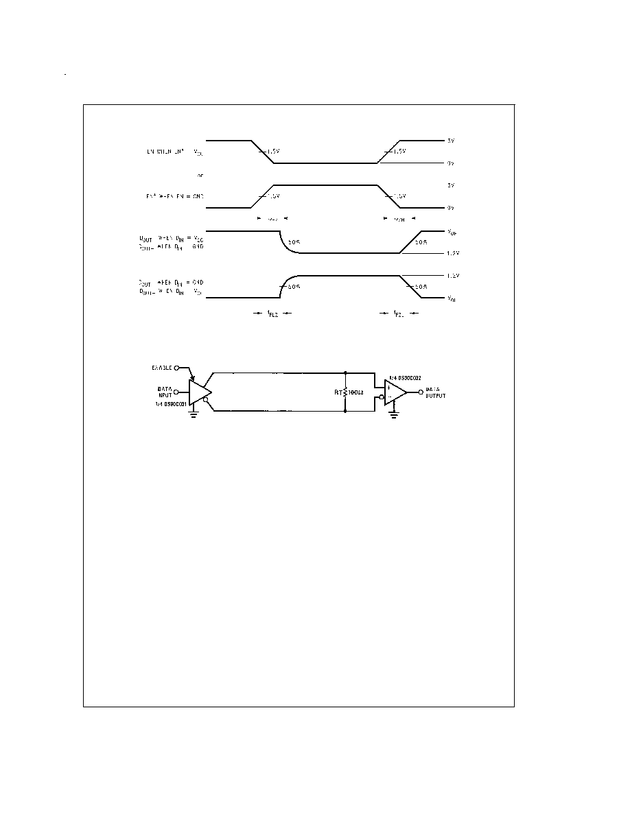
Parameter Measurement Information
(Continued)
Typical Application
Applications Information
LVDS drivers and receivers are intended to be primarily used
in an uncomplicated point-to-point configuration as is shown
in
Figure 6. This configuration provides a clean signaling en-
vironment for the quick edge rates of the drivers. The re-
ceiver is connected to the driver through a balanced media
which may be a standard twisted pair cable, a parallel pair
cable, or simply PCB traces. Typically, the characteristic im-
pedance of the media is in the range of 100
. A termination
resistor of 100
should be selected to match the media, and
is located as close to the receiver input pins as possible. The
termination resistor converts the current sourced by the
driver into a voltage that is detected by the receiver. Other
configurations are possible such as a multi-receiver configu-
ration, but the effects of a mid-stream connector(s), cable
stub(s), and other impedance discontinuities as well as
ground shifting, noise margin limits, and total termination
loading must be taken into account.
The DS90C031B differential line driver is a balanced current
source design. A current mode driver, generally speaking
has a high output impedance and supplies a constant cur-
rent for a range of loads (a voltage mode driver on the other
hand supplies a constant voltage for a range of loads). Cur-
rent is switched through the load in one direction to produce
a logic state and in the other direction to produce the other
logic state. The typical output current is a mere 3.4 mA with
a minimum of 2.5 mA, and a maximum of 4.5 mA. The cur-
rent mode requires (as discussed above) that a resistive ter-
mination be employed to terminate the signal and to com-
plete the loop as shown in
Figure 6. AC or unterminated
configurations are not allowed. The 3.4 mA loop current will
develop a differential voltage of 340 mV across the 100
ter-
mination resistor which the receiver detects with a 240 mV
minimum differential noise margin neglecting resistive line
losses (driven signal minus receiver threshold (340 mV ≠
100 mV = 240 mV). The signal is centered around +1.2V
(Driver Offset, V
OS
) with respect to ground as shown in
Fig-
ure 7. Note that the steady-state voltage (V
SS
) peak-to-peak
swing is twice the differential voltage (V
OD
) and is typically
680 mV.
The current mode driver provides substantial benefits over
voltage mode drivers, such as an RS-422 driver. Its quies-
cent current remains relatively flat versus switching fre-
quency. Whereas the RS-422 voltage mode driver increases
exponentially in most case between 20 MHz≠50 MHz. This
is due to the overlap current that flows between the rails of
the device when the internal gates switch. Whereas the cur-
rent mode driver switches a fixed current between its output
without any substantial overlap current. This is similar to
some ECL and PECL devices, but without the heavy static
I
CC
requirements of the ECL/PECL designs. LVDS requires
80% less current than similar PECL devices. AC specifica-
tions for the driver are a tenfold improvement over other ex-
isting RS-422 drivers.
The fail-safe circuitry guarantees that the outputs are en-
abled and at a logic '0' (the true output is low and the
complement output is high) when the inputs are floating.
DS100989-7
FIGURE 5. Driver TRI-STATE Delay Waveform
DS100989-8
FIGURE 6. Point-to-Point Application
www.national.com
5