 | –≠–ª–µ–∫—Ç—Ä–æ–Ω–Ω—ã–π –∫–æ–º–ø–æ–Ω–µ–Ω—Ç: DS90CR563 | –°–∫–∞—á–∞—Ç—å:  PDF PDF  ZIP ZIP |
DS90CR563/DS90CR564
LVDS 18-Bit Color Flat Panel Display (FPD) Link--
65 MHz
General Description
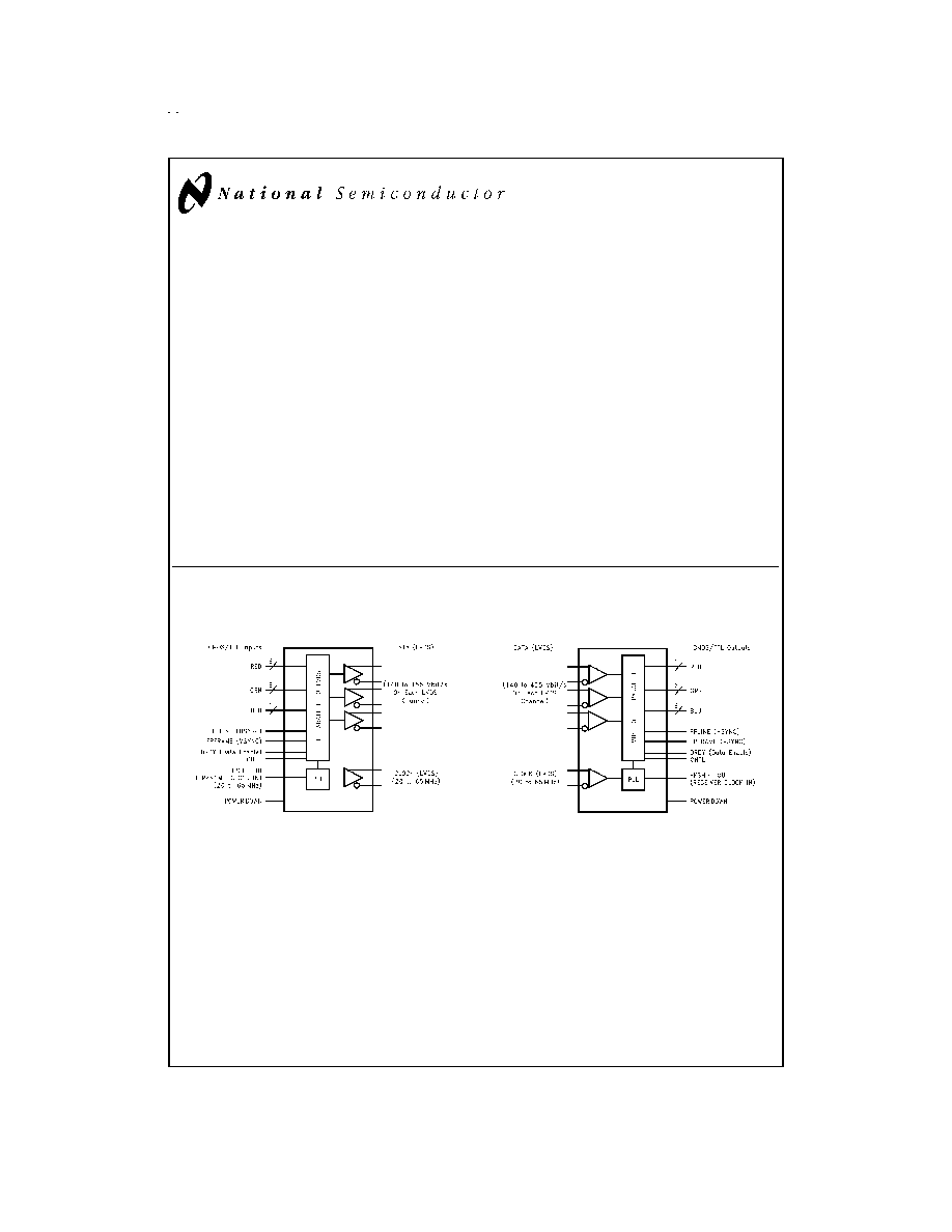
The DS90CR563 transmitter converts 21 bits of CMOS/TTL
data into three LVDS (Low Voltage Differential Signaling)
data streams. A phase-locked transmit clock is transmitted in
parallel with the data streams over a fourth LVDS link. Every
cycle of the transmit clock 21 bits of input data are sampled
and transmitted. The DS90CR564 receiver converts the
LVDS data streams back into 21 bits of CMOS/TTL data. At
a transmit clock frequency of 65 MHz, 18 bits of RGB data
and 3 bits of LCD timing and control data (FPLINE,
FPFRAME, DRDY) are transmitted at a rate of 455 Mbps per
LVDS data channel. Using a 65 MHz clock, the data through-
put is 171 Mbytes per second. These devices are offered
with rising edge data strobes for convenient interface with a
variety of graphics and LCD panel controllers.
This chipset is an ideal means to solve EMI and cable size
problems associated with wide, high speed TTL interfaces.
Features
n
20 to 65 MHz shift clk support
n
Up to 171 Mbytes/s bandwidth
n
Cable size is reduced to save cost
n
290 mV swing LVDS devices for low EMI
n
Low power CMOS design (
<
550 mW typ)
n
Power-down mode saves power (
<
0.25 mW)
n
PLL requires no external components
n
Low profile 48-lead TSSOP package
n
Rising edge data strobe
n
Compatible with TIA/EIA-644 LVDS standard
n
Single pixel per clock XGA (1024 x 768)
n
Supports VGA, SVGA, XGA and higher
n
1.3 Gbps throughput
Block Diagrams
TRI-STATE
Æ
is a registered trademark of National Semiconductor Corporation.
DS90CR563
DS012617-2
Order Number DS90CR563MTD
See NS Package Number MTD48
DS90CR564
DS012617-1
Order Number DS90CR564MTD
See NS Package Number MTD48
July 1997
DS90CR563/DS90CR564
L
VDS
18-Bit
Color
Flat
Panel
Display
(FPD)
Link
--
6
5
MHz
© 1998 National Semiconductor Corporation
DS012617
www.national.com
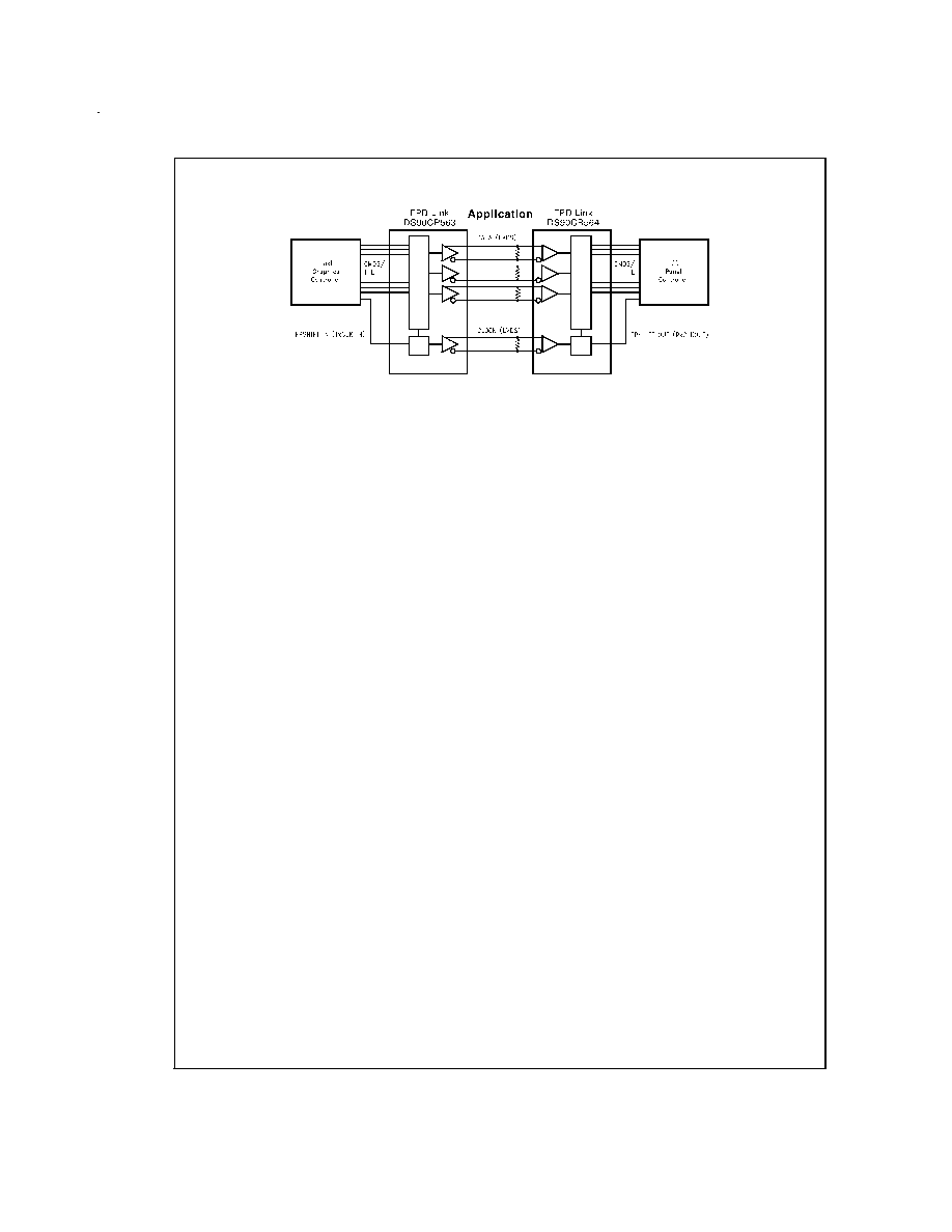
Block Diagrams
(Continued)
DS012617-3
www.national.com
2
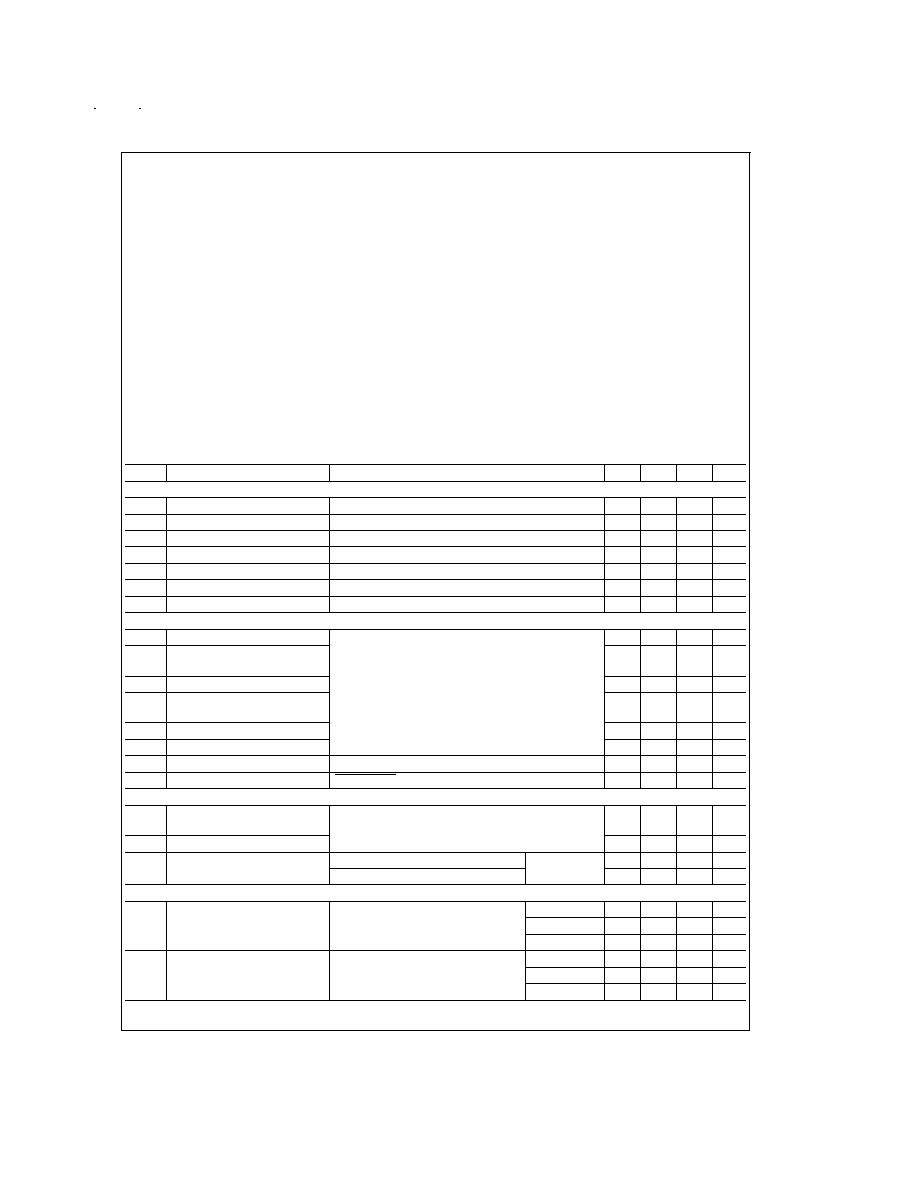
Absolute Maximum Ratings
(Note 1)
If Military/Aerospace specified devices are required,
please contact the National Semiconductor Sales Office/
Distributors for availability and specifications.
Supply Voltage (V
CC
)
-0.3V to +6V
CMOS/TTL Input Voltage
-0.3V to (V
CC
+ 0.3V)
CMOS/TTL Output Voltage
-0.3V to (V
CC
+ 0.3V)
LVDS Receiver Input Voltage
-0.3V to (V
CC
+ 0.3V)
LVDS Driver Output Voltage
-0.3V to (V
CC
+ 0.3V)
LVDS Output Short Circuit
Duration
Continuous
Junction Temperature
+150∞C
Storage Temperature
-65∞C to +150∞C
Lead Temperature
(Soldering, 4 sec)
+260∞C
Maximum Package Power Dissipation
@
+25∞C
MTD48 (TSSOP) Package:
DS90CR563
1.98W
DS90CR564
1.89W
Package Derating:
DS90CR563
16 mW/∞C above +25∞C
DS90CR564
15 mW/∞C above +25∞C
This device does not meet 2000V ESD rating (Note 4).
Recommended Operating
Conditions
Min
Nom
Max
Units
Supply Voltage (V
CC
)
4.75
5.0
5.25
V
Operating Free Air
-10
+25
+70
∞C
Temperature (T
A
)
Receiver Input Range
0
2.4
V
Supply Noise Voltage (V
CC
)
100
mV
P-P
Electrical Characteristics
Over recommended operating supply and temperature ranges unless otherwise specified
Symbol
Parameter
Conditions
Min
Typ
Max
Units
CMOS/TTL DC SPECIFICATIONS
V
IH
High Level Input Voltage
2.0
V
CC
V
V
IL
Low Level Input Voltage
GND
0.8
V
V
OH
High Level Output Voltage
I
OH
= -0.4 mA
3.8
4.9
V
V
OL
Low Level Output Voltage
I
OL
= 2 mA
0.1
0.3
V
V
CL
Input Clamp Voltage
I
CL
= -18 mA
-0.79
-1.5
V
I
IN
Input Current
V
IN
= V
CC
, GND, 2.5V or 0.4V
±
5.1
±
10
µA
I
OS
Output Short Circuit Current
V
OUT
= 0V
-120
mA
LVDS DRIVER DC SPECIFICATIONS
V
OD
Differential Output Voltage
R
L
= 100
250
290
450
mV
V
OD
Change in V
OD
between
Complementary Output States
35
mV
V
CM
Common Mode Voltage
1.1
1.25
1.375
V
V
CM
Change in V
CM
between
Complementary Output States
35
mV
V
OH
High Level Output Voltage
1.3
1.6
V
V
OL
Low Level Output Voltage
0.9
1.01
V
I
OS
Output Short Circuit Current
V
OUT
= 0V, R
L
= 100
-2.9
-5
mA
I
OZ
Output TRI-STATE
Æ
Current
Power Down = 0V, V
OUT
= 0V or V
CC
±
1
±
10
µA
LVDS RECEIVER DC SPECIFICATIONS
V
TH
Differential Input High
Threshold
V
CM
= +1.2V
+100
mV
V
TL
Differential Input Low Threshold
-100
mV
I
IN
Input Current
V
IN
= +2.4V
V
CC
= 5.5V
±
10
µA
V
IN
= 0V
±
10
µA
TRANSMITTER SUPPLY CURRENT
I
CCTW
Transmitter Supply Current,
Worst Case
R
L
= 100
, C
L
= 5 pF,
Worst Case Pattern
(
Figures 1, 3)
f = 32.5 MHz
49
63
mA
f = 37.5 MHz
51
64
mA
f = 65 MHz
70
84
mA
I
CCTG
Transmitter Supply Current,
16 Grayscale
R
L
= 100
, C
L
= 5 pF,
16 Grayscale Pattern
(
Figures 2, 3)
f = 32.5 MHz
40
55
mA
f = 37.5 MHz
41
55
mA
f = 65 MHz
55
67
mA
www.national.com
3
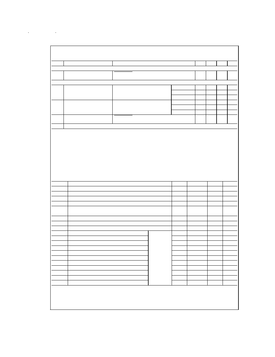
Electrical Characteristics
(Continued)
Over recommended operating supply and temperature ranges unless otherwise specified
Symbol
Parameter
Conditions
Min
Typ
Max
Units
TRANSMITTER SUPPLY CURRENT
I
CCTZ
Transmitter Supply Current,
Power Down
Power Down = Low
1
25
µA
RECEIVER SUPPLY CURRENT
I
CCRW
Receiver Supply Current,
Worst Case
C
L
= 8 pF,
Worst Case Pattern
(
Figures 1, 4)
f = 32.5 MHz
64
77
mA
f = 37.5 MHz
70
85
mA
f = 65 MHz
110
140
mA
I
CCRG
Receiver Supply Current,
16 Grayscale
C
L
= 8 pF,
16 Grayscale Pattern
(
Figures 2, 4)
f = 32.5 MHz
35
55
mA
f = 37.5 MHz
37
55
mA
f = 65 MHz
55
67
mA
I
CCRZ
Receiver Supply Current,
Power Down
Power Down = Low
1
10
µA
Note 1: "Absolute Maximum Ratings" are those values beyond which the safety of the device cannot be guaranteed. They are not meant to imply that the device
should be operated at these limits. The tables of "Electrical Characteristics" specify conditions for device operation.
Note 2: Typical values are given for V
CC
= 5.0V and T
A
= +25∞C.
Note 3: Current into device pins is defined as positive. Current out of device pins is defined as negative. Voltages are referenced to ground unless otherwise speci-
fied (except V
OD
and
V
OD
).
Note 4: ESD Rating: HBM (1.5 k
, 100 pF)
PLL V
CC
1000V
All other pins
2000V
EIAJ (0
, 200 pF)
150V
Transmitter Switching Characteristics
Over recommended operating supply and temperature ranges unless otherwise specified
Symbol
Parameter
Min
Typ
Max
Units
LLHT
LVDS Low-to-High Transition Time (
Figure 3)
0.75
1.5
ns
LHLT
LVDS High-to-Low Transition Time (
Figure 3)
0.75
1.5
ns
TCIT
TxCLK IN Transition Time (
Figure 5)
8
ns
TCCS
TxOUT Channel-to-Channel Skew (Note 5) (
Figure 6)
350
ps
TCCD
TxCLK IN to TxCLK OUT Delay
@
25∞C, V
CC
= 5.0V
3.5
8.5
ns
(
Figure 9)
TCIP
TxCLK IN Period (
Figure 7)
15
T
50
ns
TCIH
TxCLK IN High Time (
Figure 7)
0.35T
0.5T
0.65T
ns
TCIL
TxCLK IN Low Time (
Figure 7)
0.35T
0.5T
0.65T
ns
TSTC
TxIN Setup to TxCLK IN (
Figure 7)
f = 65 MHz
5
3.5
ns
THTC
TxIN Hold to TxCLK IN (
Figure 7)
2.5
1.5
ns
TPDD
Transmitter Powerdown Delay (
Figure 18)
100
ns
TPLLS
Transmitter Phase Lock Loop Set (
Figure 11)
10
ms
TPPos0
Transmitter Output Pulse Position 0 (
Figure 13)
-0.30
0
0.30
ns
TPPos1
Transmitter Output Pulse Position 1
1.70
1/7 T
clk
2.50
ns
TPPos2
Transmitter Output Pulse Position 2
3.60
2/7 T
clk
4.50
ns
TPPos3
Transmitter Output Pulse Position 3
5.90
3/7 T
clk
6.75
ns
TPPos4
Transmitter Output Pulse Position 4
8.30
4/7 T
clk
9.00
ns
TPPos5
Transmitter Output Pulse Position 5
10.40
5/7 T
clk
11.10
ns
TPPos6
Transmitter Output Pulse Position 6
12.70
6/7 T
clk
13.40
ns
Note 5: This limit based on bench characterization.
www.national.com
4
Receiver Switching Characteristics
Over recommended operating supply and temperature ranges unless otherwise specified.
Symbol
Parameter
Min
Typ
Max
Units
CLHT
CMOS/TTL Low-to-High Transition Time (
Figure 4)
2.5
4.0
ns
CHLT
CMOS/TTL High-to-Low Transition Time (
Figure 4)
2.0
3.5
ns
RCOP
RxCLK OUT Period
15
T
50
ns
RCOH
RxCLK OUT High Time
f = 65 MHz
3.8
5
ns
RCOL
RxCLK OUT Low Time
f = 65 MHz
7.8
9
ns
RSRC
RxOUT Setup to RxCLK OUT
f = 65 MHz
2.5
4.2
ns
RHRC
RxOUT Hold to RxCLK OUT
f = 65 MHz
4.0
5.2
ns
RCCD
RxCLK IN to RxCLK OUT Delay
@
25∞C, V
CC
= 5.0V
6.4
10.7
ns
(
Figure 10)
RPLLS
Receiver Phase Lock Loop Set (
Figure 12)
10
ms
RSKM
RxIN Skew Margin (Note 6) (
Figure 14)
V
CC
= 5V, T
A
=25∞C
600
ps
RPDD
Receiver Powerdown (
Figure 17)
1
µs
Note 6: Receiver Skew Margin is defined as the valid data sampling region at the receiver inputs. This margin takes into account transmitter output skew (TCCS)
and the setup and hold time (internal data sampling window), allowing for LVDS cable skew dependent on type/length and source clock (TxCLK IN) jitter.
RSKM
cable skew (type, length) + source clock jitter (cycle to cycle)
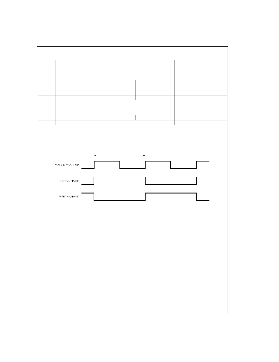
AC Timing Diagrams
DS012617-4
FIGURE 1. "Worst Case" Test Pattern
www.national.com
5