TL H 7894
LM1818
Electronically
Switched
Audio
Tape
System
April 1987
LM1818 Electronically Switched Audio Tape System
General Description
The LM1818 is a linear integrated circuit containing all of the
active electronics necessary for building a tape recorder
deck (excluding the bias oscillator) The electronic functions
on the chip include a microphone and playback preamplifi-
er record and playback amplifiers a meter driving circuit
and an automatic input level control circuit The IC features
complete internal electronic switching between the record
and playback modes of operation The multipole switch
used in previous systems to switch between record and
playback modes is replaced by a single pole switch thereby
allowing for more flexibility and reliability in the recorder de-
sign
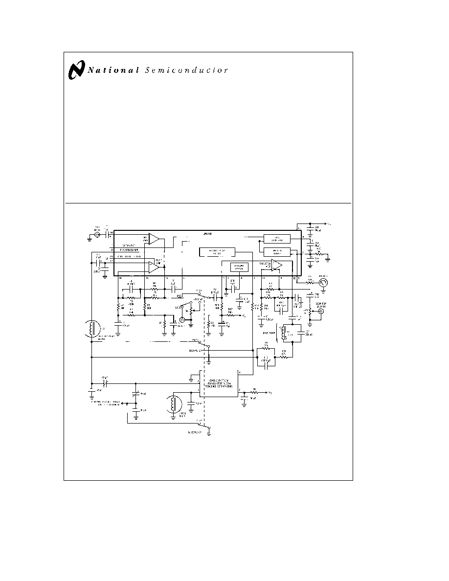
Monaural operation
Figure 9
Features
Y
Electronic record play switching
Y
85 dB power supply rejection
Y
Motional peak level meter circuitry
Y
Low noise preamplifier circuitry
Y
3 5V to 18V supply operation
Y
Provision for external low noise input transistor
Typical Applications
TL H 7894 ≠ 1
FIGURE 1 Stereo Application Circuit (Left Channel Shown) V
S
e
15V
Order Number LM1818N
See NS Package Number N20A
C1995 National Semiconductor Corporation
RRD-B30M115 Printed in U S A

Absolute Maximum Ratings
If Military Aerospace specified devices are required
please contact the National Semiconductor Sales
Office Distributors for availability and specifications
Supply Voltage
18V
Package Dissipation (Note 1)
1560 mW
Storage Temperature
b
65 C to
a
150 C
Operating Temperature
0 C to
a
70 C
Junction Temperature
150 C
Minimum Voltage on Any Pin
b
0 1 V
DC
Maximum Voltage on Pins 2 and 5
0 1 V
DC
Maximum Current Out of Pin 14
5 mA
DC
Lead Temperature (Soldering 10 sec )
260 C
Electrical Characteristics
V
CC
e
6V T
A
e
25 C See Test Circuits
(Figures 2 and 3)
Parameter
Conditions
Min
Typ
Max
Units
Operating Supply Voltage Range
3 5
18
V
DC
Supply Current
Test Circuit
(Figure 2)
5
12
mA
Turn-ON Time
Externally Programmable
50
400
ms
Playback Signal to Noise
DIN Eq (3180 and 120 ms) 20 ≠ 20 kHz
R
S
e
0 Unweighted V
REF
e
1 mV
74
dB
at 400 Hz
Record Signal to Noise
Flat Gain 20 ≠ 20 kHz R
S
e
0
ALC OFF V
REF
e
1 mV
69
dB
at 1 kHz Unweighted
Fast Turn-ON Charging Current
Pins 16 and 17
200
m
A
Record and Playback Preamplifier
f
e
100 Hz
100
dB
Open Loop Voltage Gain
Preamplifier Input Impedance
Pin 16 or Pin 17
50
kX
Preamplifier Input Referred PSRR
1 kHz
Flat Gain
85
dB
Bias Voltage on Pin 18 in Play Mode
0 5
V
or Pin 15 in Record Mode
Monitor Amplifier Input
Pins 11 and 12
0 5
m
A
Bias Current
Monitor Amplifier Open
Record or Playback f
e
100 Hz
80
dB
Loop Voltage Gain
Monitor Output Current Capability
Pins 9 and 10 Source Current Available
400
750
m
A
Monitor Amplifier Output Swing
R
L
e
10k AC Load
1 2
1 65
Vrms
THD All Amplifiers
At 1 kHz 40 dB Closed Loop Gain
0 05
%
Record-Playback Switching Time
As in Test Circuit
50
ms
Input ALC Range
D
V
IN
for DV
OUT
e
8 dB
40
dB
Input Voltage on ALC Pin for
25
mVrms
Start of ALC Action
ALC Input Impedance
2
kX
ALC Attack Time
C13
e
10 mF
7
ms
ALC Decay Time
R17
e
%
C13
e
10 mF
30
sec
Meter Output Gain
100 mVrms at 1 kHz into Pin 4
800
mV
DC
Meter Output Current Capability
2
mA
DC
Note 1
For operation in ambient temperatures above 25 C the device must be derated based on a 150 C maximum junction temperature and a thermal resistance
of 80 C W junction to ambient
2


