TL H 7148
LM3080
Operational
Transconductance
Amplifier
February 1995
LM3080
Operational Transconductance Amplifier
General Description
The LM3080 is a programmable transconductance block in-
tended to fulfill a wide variety of variable gain applications
The LM3080 has differential inputs and high impedance
push-pull outputs The device has high input impedance and
its transconductance (g
m
) is directly proportional to the am-
plifier bias current (I
ABC
)
High slew rate together with programmable gain make the
LM3080 an ideal choice for variable gain applications such
as sample and hold multiplexing filtering and multiplying
The LM3080N and LM3080AN are guaranteed from 0 C to
a
70 C
Features
Y
Slew rate (unity gain compensated) 50 V ms
Y
Fully adjustable gain 0 to g
m
R
L
limit
Y
Extended g
m
linearity 3 decades
Y
Flexible supply voltage range
g
2V to
g
18V
Y
Adjustable power consumption
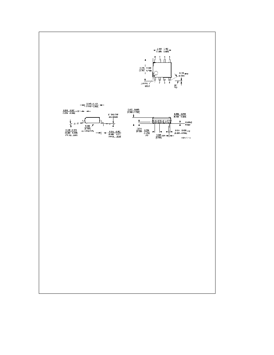
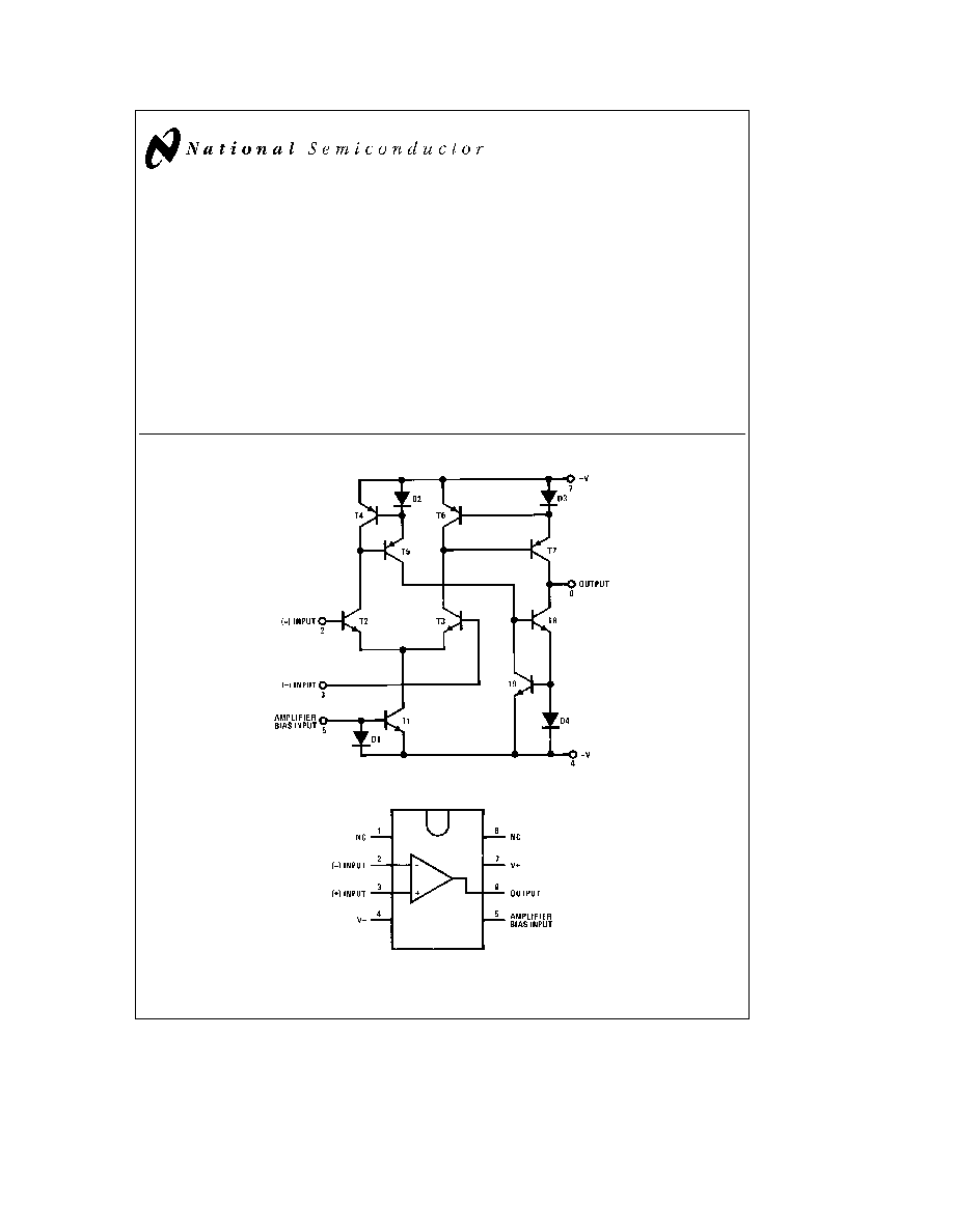
Schematic and Connection Diagrams
TL H 7148 ≠ 1
Dual-In-Line Package
TL H 7148 ≠ 2
Top View
Order Number LM3080AN LM3080M or LM3080N
See NS Package Number M08A or N08E
C1995 National Semiconductor Corporation
RRD-B30M115 Printed in U S A
Absolute Maximum Ratings
If Military Aerospace specified devices are required
please contact the National Semiconductor Sales
Office Distributors for availability and specifications
Supply Voltage (Note 2)
LM3080
g
18V
LM3080A
g
22V
Power Dissipation
250 mW
Differential Input Voltage
g
5V
Amplifier Bias Current (I
ABC
)
2 mA
DC Input Voltage
a
V
S
to
b
V
S
Output Short Circuit Duration
Indefinite
Operating Temperature Range
LM3080N or LM3080AN
0 C to
a
70 C
Storage Temperature Range
b
65 C to
a
150 C
Lead Temperature (Soldering 10 sec )
260 C
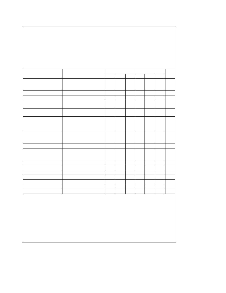
Electrical Characteristics
(Note 1)
Parameter
Conditions
LM3080
LM3080A
Units
Min
Typ
Max
Min
Typ
Max
Input Offset Voltage
0 4
5
0 4
2
mV
Over Specified Temperature Range
6
5
mV
I
ABC
e
5 mA
0 3
0 3
2
mV
Input Offset Voltage Change
5 mA
s
I
ABC
s
500 mA
0 1
0 1
3
mV
Input Offset Current
0 1
0 6
0 1
0 6
m
A
Input Bias Current
0 4
5
0 4
5
m
A
Over Specified Temperature Range
1
7
1
8
m
A
Forward Transconductance (g
m
)
6700
9600
13000
7700
9600
12000
m
mho
Over Specified Temperature Range
5400
4000
m
mho
Peak Output Current
R
L
e
0 I
ABC
e
5 mA
5
3
5
7
m
A
R
L
e
0
350
500
650
350
500
650
m
A
R
L
e
0
300
300
m
A
Over Specified Temperature Range
Peak Output Voltage
Positive
R
L
e
%
5 mA
s
I
ABC
s
500 mA
a
12
a
14 2
a
12
a
14 2
V
Negative
R
L
e
%
5 mA
s
I
ABC
s
500 mA
b
12
b
14 4
b
12
b
14 4
V
Amplifier Supply Current
1 1
1 1
mA
Input Offset Voltage Sensitivity
Positive
D
V
OFFSET
D
V
a
20
150
20
150
m
V V
Negative
D
V
OFFSET
D
V
b
20
150
20
150
m
V V
Common Mode Rejection Ratio
80
110
80
110
dB
Common Mode Range
g
12
g
14
g
12
g
14
V
Input Resistance
10
26
10
26
kX
Magnitude of Leakage Current
I
ABC
e
0
0 2
100
0 2
5
nA
Differential Input Current
I
ABC
e
0 Input
e
g
4V
0 02
100
0 02
5
nA
Open Loop Bandwidth
2
2
MHz
Slew Rate
Unity Gain Compensated
50
50
V ms
Note 1
These specifications apply for V
S
e g
15V and T
A
e
25 C amplifier bias current (I
ABC
)
e
500 mA unless otherwise specified
Note 2
Selection to supply voltage above
g
22V contact the factory
2
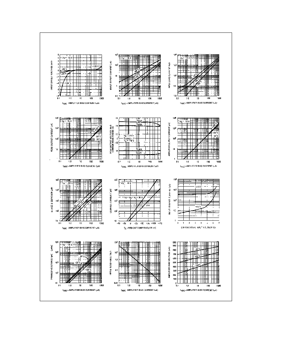
Typical Performance Characteristics
(Continued)
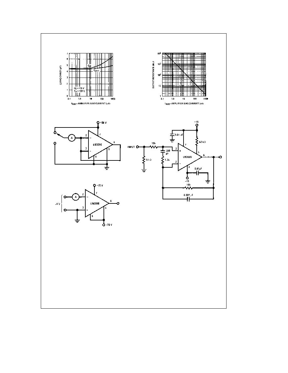
Input and Output Capacitance
TL H 7148 ≠ 4
Output Resistance
TL H 7148 ≠ 5
Leakage Current Test Circuit
TL H 7148 ≠ 6
Differential Input Current Test Circuit
TL H 7148 ≠ 7
Unity Gain Follower
TL H 7148 ≠ 8
4