 | ÐлекÑÑоннÑй компоненÑ: LM342 | СкаÑаÑÑ:  PDF PDF  ZIP ZIP |
Äîêóìåíòàöèÿ è îïèñàíèÿ www.docs.chipfind.ru
TL H 10485
LM342
Series
3-Terminal
Positive
Regulators
June 1989
LM342 Series
3-Terminal Positive Regulators
General Description
The LM342-XX series of three-terminal regulators is avail-
able with several fixed output voltages making them useful
in a wide range of applications One of these is local on card
regulation eliminating the distribution problems associated
with single point regulation The voltages available allow
these regulators to be used in logic systems instrumenta-
tion HiFi and other solid state electronic equipment Al-
though designed primarily as fixed voltage regulators these
devices can be used with external components to obtain
adjustable voltages and currents
The LM342-XX series is available in the plastic TO-202
package This package allows these regulators to deliver
over 0 25A if adequate heat sinking is provided Current lim-
iting is included to limit the peak output current to a safe
value Safe area protection for the output transistor is pro-
vided to limit internal power dissipation If internal power
dissipation becomes too high for the heat sinking provided
the thermal shutdown circuit takes over preventing the IC
from overheating
Considerable effort was expended to make the LM342-XX
series of regulators easy to use and minimize the number of
external components It is not necessary to bypass the
output although this does improve transient response Input
bypassing is needed only if the regulator is located far from
the filter capacitor of the power supply
For output voltage other than 5V 12V and 15V the LM117
series provides an output voltage range from 1 2V to 57V
Features
Y
Output current in excess of 0 25A
Y
Internal thermal overload protection
Y
No external components required
Y
Output transistor safe area protection
Y
Internal short circuit current limit
Y
Available in plastic TO-202 package
Y
Special circuitry allows start-up even if output is pulled
to negative voltage (
g
supplies)
Voltage Range
LM342-5 0
5V
LM342-12
12V
LM342-15
15V
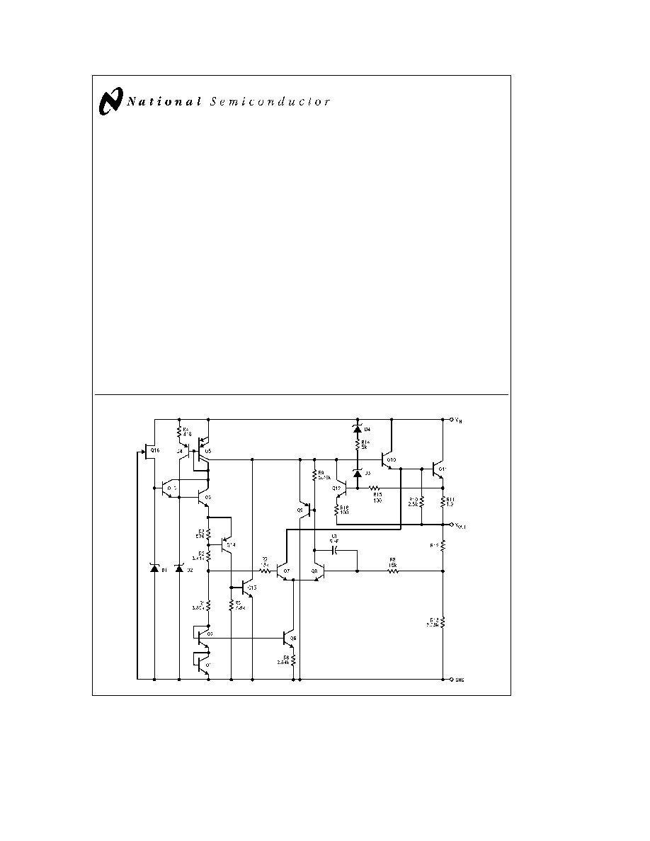
Schematic Diagram
TL H 10485 1
C1995 National Semiconductor Corporation
RRD-B30M115 Printed in U S A
Absolute Maximum Ratings
(Note 1)
If Military Aerospace specified devices are required
please contact the National Semiconductor Sales
Office Distributors for availability and specifications
Input Voltage
V
O
e
5V
30V
V
O
e
12V and 15V
35V
Internal Power Dissipation
Internally Limited
Operating Temperature Range
0 C to
a
70 C
Maximum Junction Temperature
125 C
Storage Temperature Range
b
65 C to
a
150 C
Lead Temperature (Soldering 10 sec )
300 C
ESD Susceptibility
TBD
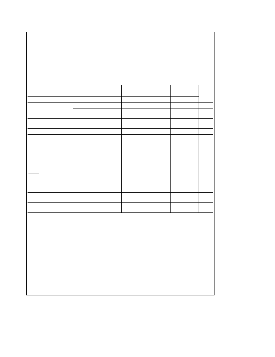
Electrical Characteristics
T
A
e
0 C to
a
70 C I
O
e
250 mA (Note 2) unless noted
Output Voltage
5V
12V
15V
Input Voltage (unless otherwise noted)
10V
19V
23V
Units
Symbol
Parameter
Conditions
Min Typ Max Min Typ Min
Min
Typ
Max
V
O
Output Voltage
T
J
e
25 C
4 8
5
5 2
11 5
12
12 5
14 4
15
15 6
V
(Note 3)
1 mA
s
I
O
s
250 mA and
4 75
5 25 11 4
12 6 14 25
15 75
V
V
MIN
s
V
IN
s
V
MAX
(7 5
s
V
IN
s
20)
(14 8
s
V
IN
s
27)
(18
s
V
IN
s
30)
D
V
O
Line Regulation
T
J
e
25 C I
O
e
250 mA
55
100
100
mV
(7 3
s
V
IN
s
25)
(14 6
s
V
IN
s
30)
(17 7
s
V
IN
s
30)
D
V
O
Load Regulation
T
J
e
25 C 1 mA
s
I
O
s
250 mA
50
120
150
mV
D
V
O
Long Term Stability
20
48
60
mV khrs
I
Q
Quiescent Current
T
J
e
25 C
6
6
6
mA
D
I
Q
Quiescent Current
T
J
e
25 C 1 mA
s
I
O
s
250 mA
0 5
0 5
0 5
mA
Change
T
J
e
25 C V
MIN
s
V
IN
s
V
MAX
1 5
1 5
1 5
mA
(7 3
s
V
IN
s
25)
(14 6
s
V
IN
s
30)
(17 7
s
V
IN
s
30)
V
n
Output Noise Voltage T
J
e
25 C f
e
10 Hz 10 kHz
40
96
120
m
V
D
V
IN
D
V
OUT
Ripple Rejection
f
e
120 Hz
50
64
44
56
42
56
dB
Input Voltage
T
J
e
25 C I
O
e
250 mA
Required to Maintain
7 3
14 6
17 7
V
Line Regulation
Thermal Resistance
P Package
15
15
15
C W
Junction to Case
Thermal Resistance
P Package
80
80
80
C W
Junction to Ambient
Note 1
Absolute Maximum Ratings indicate limits beyond which damage to the device may occur Operating Ratings indicate conditions for which the device is
intended to be functional but do not guarantee specific performance limits For guaranteed specifications and test conditions see the Electrical Characteristics
Note 2
The electrical characteristics data represent pulse test conditions with junction temperatures as shown at the initiation of tests
Note 3
The temperature coefficient of V
OUT
is typically within 0 01% V
O
C
2
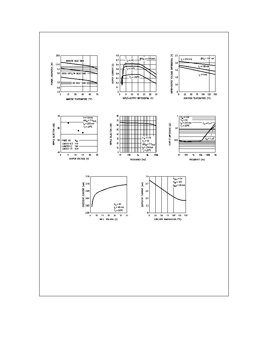
Typical Performance Characteristics
Dissipation (TO-202 Package)
Maximum Average Power
Peak Output Current
Dropout Voltage
Ripple Rejection
Ripple Rejection
Output Impedance
Quiescent Current
Quiescent Current
TL H 10485 3
3
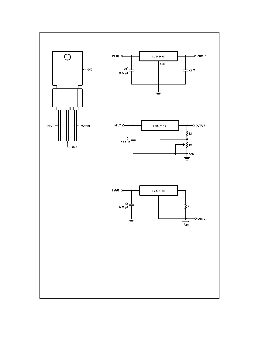
Connection Diagram
TO-202 (P) Plastic Package
TL H 10485 2
Order Number LM342P-5 0
LM342P-12 or LM342P-15
See NS Package Number P03A
Typical Applications
Fixed Output Regulator
TL H 10485 4
Required if the regulator is located far from power supply filter
Although not required C2 does improve transient response (If needed use 0 1 mF ceramic disc )
Adjustable Output Regulator
TL H 10485 5
V
O
e
5V
a
(5V R1
a
I
Q
) R2
5V R1
l
3I
Q
Load Regulation (L
R
)
e
(R1
a
R2) R1
c
(L
r
of LM342-05)
Current Regulator
TL H 10485 6
I
OUT
e
V
2
b
3
R1
a
I
Q
D
I
Q
s
1 5 mA over line and load changes
4
Typical Applications
(Continued)
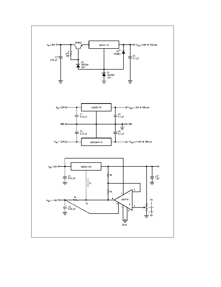
High Output Voltage Regulator
TL H 10485 7
Necessary if regulator is located far from the power supply filter
D3 aids in full load start-up and protects the regulator during short circuits from high input to output voltage differentials
g
15V 250 mA Dual Power Supply
TL H 10485 8
Variable Output Regulator 0 5V 18V
V
OUT
e
V
G
a
5V R1
e
(
b
V
IN
I
Q
LM342)
V
OUT
e
5V(R2 R4) for (R2
a
R3)
e
(R4
a
R5)
A 0 5V output will correspond to (R2 R4)
e
0 1 (R3 R4)
e
0 9
TL H 10485 9
Solid tantalum
5