 | –≠–Ľ–Ķ–ļ—ā—Ä–ĺ–Ĺ–Ĺ—č–Ļ –ļ–ĺ–ľ–Ņ–ĺ–Ĺ–Ķ–Ĺ—ā: LM3420 | –°–ļ–į—á–į—ā—Ć:  PDF PDF  ZIP ZIP |
LM3420-4.2, -8.2, -8.4, -12.6, -16.8
Lithium-Ion Battery Charge Controller
General Description
The LM3420 series of controllers are monolithic integrated
circuits designed for charging and end-of-charge control for
Lithium-Ion rechargeable batteries. The LM3420 is available
in five fixed voltage versions for one through four cell charger
applications (4.2V, 8.2V/8.4V, 12.6V and 16.8V respec-
tively).
Included in a very small package is an (internally compen-
sated) op amp, a bandgap reference, an NPN output transis-
tor, and voltage setting resistors. The amplifier's inverting in-
put
is
externally
accessible
for
loop
frequency
compensation. The output is an open-emitter NPN transistor
capable of driving up to 15 mA of output current into external
circuitry.
A trimmed precision bandgap reference utilizes temperature
drift curvature correction for excellent voltage stability over
the operating temperature range. Available with an initial tol-
erance of 0.5% for the A grade version, and 1% for the stan-
dard version, the LM3420 allows for precision end-of-charge
control for Lithium-Ion rechargeable batteries.
The LM3420 is available in a sub-miniature 5-lead SOT23-5
surface mount package thus allowing very compact designs.
Features
n
Voltage options for charging 1, 2, 3 or 4 cells
n
Tiny SOT23-5 package
n
Precision (0.5%) end-of-charge control
n
Drive capability for external power stage
n
Low quiescent current, 85 ĶA (typ.)
Applications
n
Lithium-Ion battery charging
n
Suitable for linear and switching regulator charger
designs
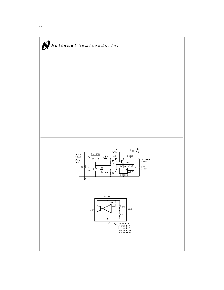
Typical Application and Functional Diagram
SIMPLE SWITCHER
ģ
is a registered trademark of National Semiconductor Corporation.
DS012359-1
Typical Constant Current/Constant Voltage
Li-Ion Battery Charger
DS012359-2
LM3420 Functional Diagram
May 1998
LM3420-4.2,
-8.2,
-8.4,
-12.6,
-16.8
Lithium-Ion
Battery
Charge
Controller
© 1999 National Semiconductor Corporation
DS012359
www.national.com
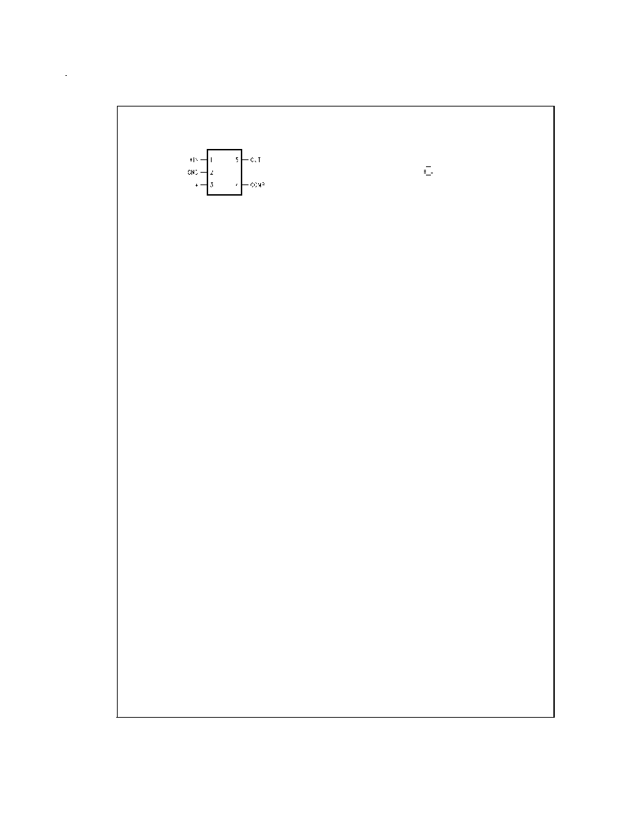
Connection Diagrams and Order Information
5-Lead Small Outline Package (M5)
DS012359-3
*No internal connection, but should be soldered to PC board for best heat
transfer.
Top View
Actual Size
DS012359-4
For Ordering Information
See
Figure 1 in this Data Sheet
See NS Package Number MA05B
www.national.com
2
Absolute Maximum Ratings
(Note 1)
If Military/Aerospace specified devices are required,
please contact the National Semiconductor Sales Office/
Distributors for availability and specifications.
Input Voltage V(IN)
20V
Output Current
20 mA
Junction Temperature
150įC
Storage Temperature
-65įC to +150įC
Lead Temperature
Vapor Phase (60 seconds)
+215įC
Infrared (15 seconds)
+220įC
Power Dissipation (T
A
= 25įC)
(Note 2)
300 mW
ESD Susceptibility (Note 3)
Human Body Model
1500V
See AN-450 "Surface Mounting Methods and Their Effect
on Product Reliability" for methods on soldering
surface-mount devices.
Operating Ratings
(Notes 1, 2)
Ambient Temperature Range
-40įC
T
A
+85įC
Junction Temperature Range
-40įC
T
J
+125įC
Output Current
15 mA
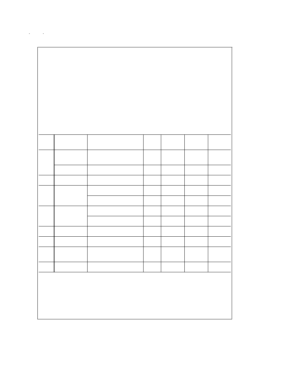
LM3420-4.2
Electrical Characteristics
Specifications with standard type face are for T
J
= 25įC, and those with boldface type apply over full Operating Tempera-
ture Range. Unless otherwise specified, V(IN) = V
REG
, V
OUT
= 1.5V.
Symbol
Parameter
Conditions
Typical
LM3420A-4.2
LM3420-4.2
Units
(Note 4)
Limit
Limit
(Limits)
(Note 5)
(Note 5)
V
REG
Regulation Voltage
I
OUT
= 1 mA
4.2
V
4.221/4.242
4.242/4.284
V(max)
4.179/4.158
4.158/4.116
V(min)
Regulation Voltage
I
OUT
= 1 mA
Ī
0.5/
Ī
1
Ī
1/
Ī
2
%(max)
Tolerance
I
q
Quiescent Current
I
OUT
= 1 mA
85
ĶA
110/115
125/150
ĶA(max)
G
m
Transconductance
20 ĶA
I
OUT
1 mA
3.3
mA/mV
I
OUT
/
V
REG
V
OUT
= 2V
1.3/0.75
1.0/0.50
mA/mV(min)
1 mA
I
OUT
15 mA
6.0
mA/mV
V
OUT
= 2V
3.0/1.5
2.5/1.4
mA/mV(min)
A
V
Voltage Gain
1V
V
OUT
V
REG
- 1.2V (-1.3)
1000
V/V
V
OUT
/
V
REG
R
L
= 200
(Note 6)
550/250
450/200
V/V(min)
1V
V
OUT
V
REG
- 1.2V (-1.3)
3500
V/V
R
L
= 2 k
1500/900
1000/700
V/V(min)
V
SAT
Output Saturation
V(IN) = V
REG
+100 mV
1.0
V
(Note 7)
I
OUT
= 15 mA
1.2/1.3
1.2/1.3
V(max)
I
L
Output Leakage
V(IN) = V
REG
-100 mV
0.1
ĶA
Current
V
OUT
= 0V
0.5/1.0
0.5/1.0
ĶA(max)
R
f
Internal Feedback
75
k
Resistor (Note 8)
94
94
k
(max)
56
56
k
(min)
E
n
Output Noise
I
OUT
= 1 mA, 10 Hz
f
10 kHz
70
ĶV
RMS
Voltage
www.national.com
3
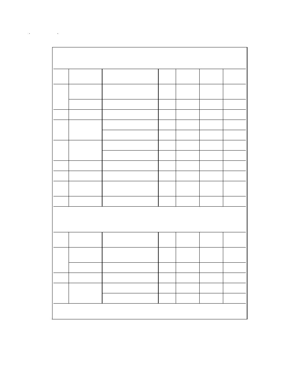
LM3420-8.2
Electrical Characteristics
Specifications with standard type face are for T
J
= 25įC, and those with boldface type apply over full Operating Tempera-
ture Range. Unless otherwise specified, V(IN) = V
REG
, V
OUT
= 1.5V.
Symbol
Parameter
Conditions
Typical
LM3420A-8.2
LM3420-8.2
Units
(Note 4)
Limit
Limit
(Limits)
(Note 5)
(Note 5)
V
REG
Regulation Voltage
I
OUT
= 1 mA
8.2
V
8.241/8.282
8.282/8.364
V(max)
8.159/8.118
8.118/8.036
V(min)
Regulation Voltage
I
OUT
= 1 mA
Ī
0.5/
Ī
1
Ī
1/
Ī
2
%(max)
Tolerance
I
q
Quiescent Current
I
OUT
= 1 mA
85
ĶA
110/115
125/150
ĶA(max)
G
m
Transconductance
20 ĶA
I
OUT
1 mA
3.3
mA/mV
I
OUT
/
V
REG
V
OUT
= 6V
1.3/0.75
1.0/0.50
mA/mV(min)
1 mA
I
OUT
15 mA
6.0
mA/mV
V
OUT
= 6V
3.0/1.5
2.5/1.4
mA/mV(min)
A
V
Voltage Gain
1V
V
OUT
V
REG
- 1.2V (-1.3)
1000
V/V
V
OUT
/
V
REG
R
L
= 470
(Note 6)
550/250
450/200
V/V(min)
1V
V
OUT
V
REG
- 1.2V (-1.3)
3500
V/V
R
L
= 5 k
1500/900
1000/700
V/V(min)
V
SAT
Output Saturation
V(IN) = V
REG
+100 mV
1.0
V
(Note 7)
I
OUT
= 15 mA
1.2/1.3
1.2/1.3
V(max)
I
L
Output Leakage
V(IN) = V
REG
-100 mV
0.1
ĶA
Current
V
OUT
= 0V
0.5/1.0
0.5/1.0
ĶA(max)
R
f
Internal Feedback
176
k
Resistor (Note 8)
220
220
k
(max)
132
132
k
(min)
E
n
Output Noise
I
OUT
= 1 mA, 10 Hz
f
10 kHz
140
ĶV
RMS
Voltage
LM3420-8.4
Electrical Characteristics
Specifications with standard type face are for T
J
= 25įC, and those with boldface type apply over full Operating Tempera-
ture Range. Unless otherwise specified, V(IN) = V
REG
, V
OUT
= 1.5V.
Symbol
Parameter
Conditions
Typical
LM3420A-8.4
LM3420-8.4
Units
(Note 4)
Limit
Limit
(Limits)
(Note 5)
(Note 5)
V
REG
Regulation Voltage
I
OUT
= 1 mA
8.4
V
8.442/8.484
8.484/8.568
V(max)
8.358/8.316
8.316/8.232
V(min)
Regulation Voltage
I
OUT
= 1 mA
Ī
0.5/
Ī
1
Ī
1/
Ī
2
%(max)
Tolerance
I
q
Quiescent Current
I
OUT
= 1 mA
85
ĶA
110/115
125/150
ĶA(max)
G
m
Transconductance
20 ĶA
I
OUT
1 mA
3.3
mA/mV
I
OUT
/
V
REG
V
OUT
= 6V
1.3/0.75
1.0/0.50
mA/mV(min)
1 mA
I
OUT
15 mA
6.0
mA/mV
V
OUT
= 6V
3.0/1.5
2.5/1.4
mA/mV(min)
www.national.com
4

LM3420-8.4
Electrical Characteristics
(Continued)
Specifications with standard type face are for T
J
= 25įC, and those with boldface type apply over full Operating Tempera-
ture Range. Unless otherwise specified, V(IN) = V
REG
, V
OUT
= 1.5V.
Symbol
Parameter
Conditions
Typical
LM3420A-8.4
LM3420-8.4
Units
(Note 4)
Limit
Limit
(Limits)
(Note 5)
(Note 5)
A
V
Voltage Gain
1V
V
OUT
V
REG
- 1.2V (-1.3)
1000
V/V
V
OUT
/
V
REG
R
L
= 470
(Note 6)
550/250
450/200
V/V(min)
1V
V
OUT
V
REG
- 1.2V (-1.3)
3500
V/V
R
L
= 5 k
1500/900
1000/700
V/V(min)
V
SAT
Output Saturation
V(IN) = V
REG
+100 mV
1.0
V
(Note 7)
I
OUT
= 15 mA
1.2/1.3
1.2/1.3
V(max)
I
L
Output Leakage
V(IN) = V
REG
-100 mV
0.1
ĶA
Current
V
OUT
= 0V
0.5/1.0
0.5/1.0
ĶA(max)
R
f
Internal Feedback
181
k
Resistor (Note 8)
227
227
k
(max)
135
135
k
(min)
E
n
Output Noise
I
OUT
= 1 mA, 10 Hz
f
10 kHz
140
ĶV
RMS
Voltage
LM3420-12.6
Electrical Characteristics
Specifications with standard type face are for T
J
= 25įC, and those with boldface type apply over full Operating Temperature
Range. Unless otherwise specified, V(IN) = V
REG
, V
OUT
= 1.5V.
Symbol
Parameter
Conditions
Typical
LM3420A-12.6
LM3420-12.6
Units
(Note 4)
Limit
Limit
(Limits)
(Note 5)
(Note 5)
V
REG
Regulation Voltage
I
OUT
= 1 mA
12.6
V
12.663/12.726
12.726/12.852
V(max)
12.537/12.474
12.474/12.348
V(min)
Regulation Voltage
I
OUT
= 1 mA
Ī
0.5/
Ī
1
Ī
1/
Ī
2
%(max)
Tolerance
I
q
Quiescent Current
I
OUT
= 1 mA
85
ĶA
110/115
125/150
ĶA(max)
G
m
Transconductance
20 ĶA
I
OUT
1 mA
3.3
mA/mV
I
OUT
/
V
REG
V
OUT
= 10V
1.3/0.75
1.0/0.5
mA/mV(min)
1 mA
I
OUT
15 mA
6.0
mA/mV
V
OUT
= 10V
3.0/1.5
2.5/1.4
mA/mV(min)
A
V
Voltage Gain
1V
V
OUT
V
REG
- 1.2V (-1.3)
1000
V/V
V
OUT
/
V
REG
R
L
= 750
(Note 6)
550/250
450/200
V/V(min)
1V
V
OUT
V
REG
- 1.2V (-1.3)
3500
V/V
R
L
= 10 k
1500/900
1000/700
V/V(min)
V
SAT
Output Saturation
V(IN) = V
REG
+100 mV
1.0
V
(Note 7)
I
OUT
= 15 mA
1.2/1.3
1.2/1.3
V(max)
I
L
Output Leakage
V(IN) = V
REG
-100 mV
0.1
ĶA
Current
V
OUT
= 0V
0.5/1.0
0.5/1.0
ĶA(max)
R
f
Internal Feedback
287
k
Resistor (Note 8)
359
359
k
(max)
215
215
k
(min)
E
n
Output Noise
Voltage
I
OUT
= 1 mA, 10 Hz
f
10 kHz
210
ĶV
RMS
www.national.com
5