 | –≠–ª–µ–∫—Ç—Ä–æ–Ω–Ω—ã–π –∫–æ–º–ø–æ–Ω–µ–Ω—Ç: LM3622 | –°–∫–∞—á–∞—Ç—å:  PDF PDF  ZIP ZIP |

LM3622
Lithium-Ion Battery Charger Controller
General Description
The LM3622 is a charge controller for Lithium-Ion batteries.
This monolithic integrated circuit accurately controls an ex-
ternal pass transistor for precision Lithium-Ion battery charg-
ing. The LM3622 provides a constant voltage or constant
current (CVCC) configuration that changes, as necessary, to
optimally charge lithium-ion battery cells. Voltage charging
versions (4.1V, 4.2V, 8.2V, and 8.4V) are available for one or
two cell battery packs and for coke or graphite anode battery
chemistry.
The LM3622 accepts input voltages from 4.5V to 24V. Con-
troller accuracy over temperature is
±
30mV/cell for A grade
and
±
50mV/cell for the standard grade. No precision exter-
nal resistors are required. Furthermore, the LM3622's propri-
etary output voltage sensing circuit drains less than 200nA
from the battery when the input source is disconnected.
The LM3622 circuitry includes functions for regulating the
charge voltage with a temperature compensated bandgap
reference and regulating the current with an external sense
resistor. The internal bandgap insures excellent controller
performance over the operating temperature and input sup-
ply range.
The LM3622 can sink 15mA minimum at the EXT pin to drive
the base of an external PNP pass transistor. It also has
low-voltage battery threshold circuitry that removes this drive
when the cell voltage drops below a preset limit. The LV
SEL
pin programs this threshold voltage to either 2.7V/cell or
2.15V/cell. The low-voltage detection, which is a user en-
abled feature, provides an output signal that can be used to
enable a
wake up charge
source automatically to precon-
dition a deeply discharged pack.
The LM3622 is available in a standard 8-lead SOIC surface
mount package.
Features
n
Versions for charging of 1 cell (4.1V or 4.2V) or 2 cells
(8.2V or 8.4V)
n
Versions for coke or graphite anode
n
Precision (
±
30mV/cell) end-of-charge control
n
Wide input range: 4.5V-24V
n
Low battery drain leakage: 200nA
n
15 mA available to drive low cost PNP
Applications
n
Cellular phone cradle charger
n
PDA/Notebook cradle charger
n
Camcorder cradle charger
Typical Application
DS100974-1
February 2000
LM3622
Lithium-Ion
Battery
Charger
Controller
© 2000 National Semiconductor Corporation
DS100974
www.national.com

Connection Diagram
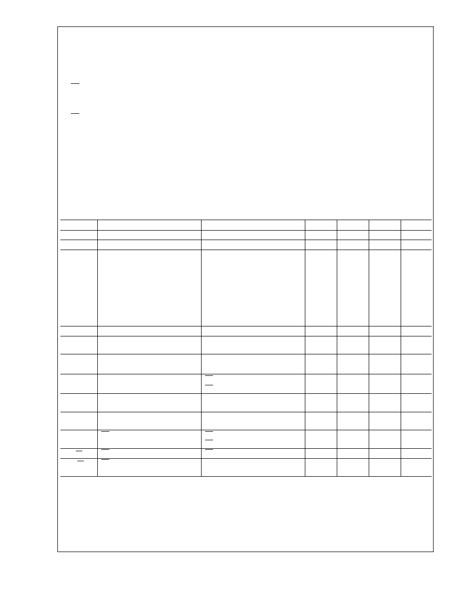
Pin Description
Pin No.
Name
I/O
Description
1
LV
SEL
Input
Low-voltage detection threshold Select. The threshold is 2.15V/cell when this pin is
pulled low to GND and 2.70V/cell when it is pulled up to V
CC
. The battery voltage is
sensed between CEL and CS pins.
2
LV
ENB
Input
Low-voltage detection Enable. The low-voltage detection is enabled when this pin is
pulled Low to GND. Pulling this pin HIGH to V
CC
disables the low-voltage detection.
3
LV
Output
Output of the low-voltage detection. This pin is a NPN open-collector output that
goes to low impedance state when LV
ENB
is pulled LOW and the battery voltage is
below the threshold set by LV
SEL
. LV stays in HIGH impedance state at any battery
voltage when LV
ENB
is pulled HIGH to V
CC
. LV can be used for turning on a low
current source to recondition a deeply depleted battery.
4
GND
Ground
IC common.
5
CS
Input
Input for battery charge current and battery negative-terminal voltage sensing.
Battery charging current is sensed through an external resistor, R
CS
, connected
between the battery's negative terminal and GND. The maximum charge current is
regulated to a value of 100mV/R
CS
.
6
CEL
Input
Battery positive-terminal voltage sensing.
7
EXT
Output
Output of the controller for driving a PNP transistor or P-MOSFET. The controller
modulates the current sinking into this pin to control the regulation of either the
charge current or the battery voltage.
8
V
CC
Power Supply
IC power supply
8-Lead Surface Mount Package
DS100974-2
Refer to the Ordering Information Table in this Datasheet for Specific Part Number
See NS Package M08A
LM3622
www.national.com
2

Ordering Information
Voltage
Grade
Accuracy
Order Information
Supplied As
4.1V
A
±
30mV
LM3622AM-4.1
95 unit increments in rail
4.1V
A
±
30mV
LM3622AMX-4.1
2500 unit increments in tape and reel
4.1V
Standard
±
50mV
LM3622M-4.1
95 unit increments in rail
4.1V
Standard
±
50mV
LM3622MX-4.1
2500 unit increments in tape and reel
4.2V
A
±
30mV
LM3622AM-4.2
95 unit increments in rail
4.2V
A
±
30mV
LM3622AMX-4.2
2500 unit increments in tape and reel
4.2V
Standard
±
50mV
LM3622M-4.2
95 unit increments in rail
4.2V
Standard
±
50mV
LM3622MX-4.2
2500 unit increments in tape and reel
8.2V
A
±
60mV
LM3622AM-8.2
95 unit increments in rail
8.2V
A
±
60mV
LM3622AMX-8.2
2500 unit increments in tape and reel
8.2V
Standard
±
100mV
LM3622M-8.2
95 unit increments in rail
8.2V
Standard
±
100mV
LM3622MX-8.2
2500 unit increments in tape and reel
8.4V
A
±
60mV
LM3622AM-8.4
95 unit increments in rail
8.4V
A
±
60mV
LM3622AMX-8.4
2500 unit increments in tape and reel
8.4V
Standard
±
100mV
LM3622M-8.4
95 unit increments in rail
8.4V
Standard
±
100mV
LM3622MX-8.4
2500 unit increments in tape and reel
LM3622
www.national.com
3
Absolute Maximum Ratings
(Note 1)
If Military/Aerospace specified devices are required,
please contact the National Semiconductor Sales Office/
Distributors for availability and specifications.
Supply Voltage (V
CC
)
-0.3 to 24V
LV
-0.3 to 24V
EXT (Note 2)
-0.3 to 24V
LV
SEL
-0.3 to 24V
LV
ENB
-0.3 to 24V
ESD Susceptibility (Note 3)
2500V
Storage Temperature
-40∞C to +125∞C
Lead Temp. Soldering
Vapor Phase (60 sec.)
Infrared (15 sec.)
215∞C
220∞C
Power Dissipation (T
A
= 25∞C)
(Note 4)
Max. Package Dissipation
350mW
Operating Ratings
(Note 1)
Supply Voltage (V
CC
)
4.5V to 24V
Ambient Temperature Range
-20∞C to 70∞C
Junction Temperature Range
-20∞C to 85∞C
Thermal Resistance,
JA
SOIC-8
170∞C/W
Electrical Characteristics
LM3622-XX
Unless otherwise specified V
CC
= 5V/Cell T
A
=T
J
= 25∞C. Limits with standard typeface apply for T
J
= 25∞C, and limits in bold-
face type apply over the indicated temperature range.
Symbol
Parameter
Conditions
Min
Typ
Max
Units
V
CC
Operating power supply range
4.5
24.0
V
I
CC
Quiescent Current
210
µA
V
CEL
Regulation Voltage
LM3622A-4.1
LM3622A-8.2
LM3622A-4.2
LM3622A-8.4
LM3622-4.1
LM3622-8.2
LM3622-4.2
LM3622-8.4
T
J
= 0∞C to +70∞C
V
CC
= 4.5V/cell (Note 5)
4.070
8.140
4.170
8.340
4.050
8.100
4.150
8.300
4.100
8.200
4.200
8.400
4.100
8.200
4.200
8.400
4.130
8.260
4.230
8.460
4.150
8.300
4.250
8.500
V
V
V
V
V
V
V
Long Term Stability
(Note 6)
0.02
%
V
CS
Current limit threshold at CS pin
V
CEL
= 4V for LM3622-4.X
V
CEL
= 8V for LM3622-8.X
90
100
110
mV
I
CEL
Current in CEL pin
V
CC
Supply connected
25
µA
V
CC
Supply Open
200
nA
LVth
Low voltage detect threshold
(between pins CS and GND)
LV
ENB
= 0V and LV
SEL
= 0V
2.00
2.15
2.30
V/Cell
LV
ENB
= 0V and LV
SEL
= V
CC
2.55
2.70
2.85
V/Cell
I
EXT
EXT pin output sink current
V
EXT
= 4V for LM3622-4.X
V
EXT
= 8V for LM3622-8.X
15
25
mA
I
IN1
LV
SEL
input current
LV
SEL
= 5V, LM3622-4.X
LV
SEL
= 10V, LM3622-8.X
20
50
µA
I
IN2
LV
ENB
input current
LV
ENB
= 5V, LM3622-4.X
LV
ENB
= 10V, LM3622-8.X
20
50
µA
I
LV
LV pin leakage current
LV = 5V/Cell
250
nA
V
LV
LV pin saturation voltage
I
SINK
= 1mA
T
J
= -20∞C to 85∞C
0.25
0.40
V
Note 1: Absolute Maximum Ratings indicate limits beyond which damage to the device may occur. Operating Ratings indicate conditions for which the device is in-
tended to be functional, but do not guarantee specific performance limits. For guaranteed specifications and test conditions, see the Electrical Characteristics.
Note 2: V
EXT
is not allowed to exceed (V
CC
+ 0.3V) or damage to the device may occur.
Note 3: Rating is for the human body model, a 100 pF capacitor discharged through a 1.5k
resistor into each pin.
Note 4: The maximum power dissipation must be de-rated at elevated temperatures and is limited by T
JMAX
(maximum junction temperature),
JA
(junction-to-ambient thermal resistance) and T
A
(ambient temperature). The maximum power dissipation at any temperature is: PDiss
MAX
= (T
JMAX
- T
A
) /
JA
up
to the value listed in the Absolute Maximum Ratings.
Note 5: Limits reflect initial accuracy.
Note 6: T
J
= 85∞C, 1000 hours. Activation energy of 0.78eV used.
LM3622
www.national.com
4

Typical Performance Characteristics
Unless otherwise specified, T
A
= 25∞C.
Output Voltage Regulation
Vs V
CC
DS100974-5
Current Sense Voltage Regulation
Vs V
CC
DS100974-8
Current Sense Voltage Regulation
Vs Temperature
DS100974-4
Output Drive Current Vs V
CC
DS100974-6
Output Drive Current Vs V
CC
DS100974-7
Quiescent Current Vs V
CC
DS100974-3
LM3622
www.national.com
5