
LM4917
Ground-Referenced, 95mW Stereo Headphone Amplifier
General Description
The LM4917 is a stereo, output capacitor-less headphone
amplifier capable of delivering 95mW of continuous average
power into a 16
load with less than 1% THD+N from a
single 3V power supply.
The LM4917 provides high quality audio reproduction with
minimal external components. A ground referenced output
eliminates the output coupling capacitors typically required
by single-ended loads, reducing component count, cost and
board space consumption. This makes the LM4917 ideal for
mobile phones and other portable equipment where board
space is at a premium. Eliminating the output coupling ca-
pacitors also improves low frequency response.
The LM4917 operates from a single 1.4V to 3.6V power
supply, features low 0.02% THD+N and 70dB PSRR. Inde-
pendent right/left channel low-power shutdown controls pro-
vide power saving flexibility for mono/stereo applications.
Superior click and pop suppression eliminates audible tran-
sients during start up and shutdown. Short circuit and ther-
mal overload protection protects the device during fault con-
ditions.
Key Specifications
j
Improved PSRR at 1kHz
70dB (typ)
j
Power Output at V
DD
= 3V,
R
L
= 16
, THD % 1%
95mW (typ)
j
Shutdown Current
0.01�A (typ)
Features
n
Ground referenced outputs
n
High PSRR
n
Available in space-saving TSSOP package
n
Ultra low current shutdown mode
n
Improved pop & click circuitry eliminates noises during
turn-on and turn-off transitions
n
1.4 � 3.6V operation
n
No output coupling capacitors, snubber networks,
bootstrap capacitors
n
Shutdown either channel independently
Applications
n
Notebook PCs
n
Desktop PCs
n
Mobile Phone
n
PDAs
n
Portable electronic devices
Block Diagram
Boomer
�
is a registered trademark of National Semiconductor Corporation.
200893B8
FIGURE 1. Circuit Block Diagram
November 2004
LM4917
Ground-Referenced,
95mW
Stereo
Headphone
Amplifier
� 2004 National Semiconductor Corporation
DS200893
www.national.com
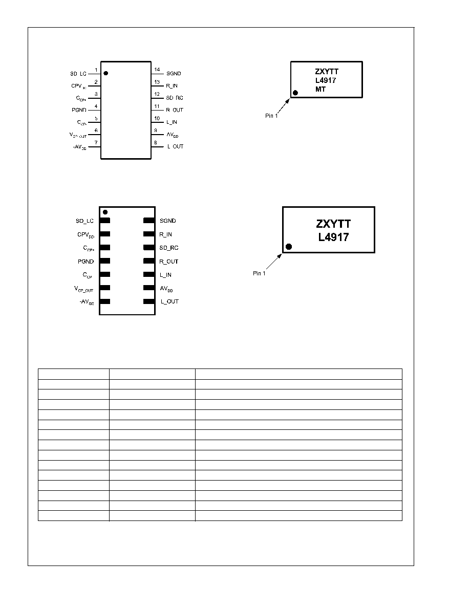
Connection Diagrams
TSSOP Package
TSSOP Marking
200893A4
Top View
Order Number LM4917MT
See NS Package Number MTC14
200893B7
Z - Assembly Plant Code
XY - Date Code
TT - Traceability
LLP Package
LLP Marking
200893C0
Top View
Order Number LM4917SD
See NS Package Number SDA14A
200893C4
Z - Assembly Plant Code
XY - Date Code
TT - Traceability
Pin Descriptions
Pin
Name
Function
1
SD_LC
Active_Low Shutdown, Left Channel
2
CP
VDD
Charge Pump Power Supply
3
C
CP+
Positive Terminal-Charge Pump Flying Capacitor
4
PGND
Power Ground
5
C
CP-
Negative Terminal- Charge Pump Flying Capacitor
6
V
CP_OUT
Charge Pump Output
7
-AV
DD
Negative Power Supply-Amplifier
8
L_OUT
Left Channel Output
9
AV
DD
Positive Power Supply-Amplifier
10
L_IN
Left Channel Input
11
R_OUT
Right Channel Output
12
SD_RC
Active_Low Shutdown, Right Channel
13
R_IN
Right Channel Input
14
SGND
Signal Ground
LM4917
www.national.com
3
Absolute Maximum Ratings
(Note 2)
If Military/Aerospace specified devices are required,
please contact the National Semiconductor Sales Office/
Distributors for availability and specifications.
Supply Voltage
4.0V
Storage Temperature
-65�C to +150�C
Input Voltage
-0.3V to V
DD
+ 0.3V
Power Dissipation (Note 3)
Internally Limited
ESD Susceptibility (Note 4)
2000V
ESD Susceptibility (Note 5)
200V
Junction Temperature
150�C
Thermal Resistance
JC
(TSSOP)
40�C/W
JA
(TSSOP)
109�C/W
Operating Ratings
Temperature Range
T
MIN
T
A
T
MAX
-40�C
T
A
85�C
Supply Voltage (V
DD
)
1.4V
V
CC
3.6V
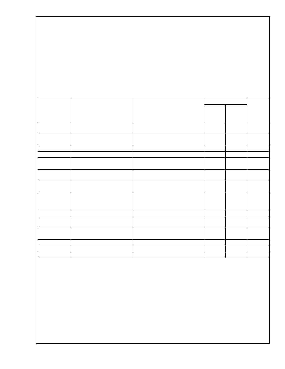
Electrical Characteristics V
DD
= 3V
(Notes 1, 2)
The following specifications apply for V
DD
= 3V, A
V
= 1, and 16
load unless otherwise specified. Limits apply to T
A
= 25�C.
Symbol
Parameter
Conditions
LM4917
Units
(Limits)
Typ
(Note 6)
Limit
(Notes 7,
8)
I
DD
Quiescent Power Supply Current
V
IN
= 0V, I
O
= 0A, both channels
enabled
11
20
mA (max)
V
IN
= 0V, I
O
= 0A, one channel
enabled
9
mA
I
SD
Shutdown Current
V
SD_LC
= V
SD_RC
= GND
0.01
1
�A (max)
V
OS
Output Offset Voltage
R
L
= 32
1
10
mV (max)
P
O
Output Power
THD+N = 1% (max); f = 1kHz, R
L
=
16
95
50
mW (min)
THD+N = 1% (max); f = 1kHz, R
L
=
32
82
mW
THD+N
Total Harmonic Distortion + Noise P
O
= 50mW, f = 1kHz, R
L
= 32
(A-weighted) single channel
0.02
%
PSRR
Power Supply Rejection Ratio
V
RIPPLE
= 200mV sine p-p,
f = 1kHz
f = 20kHz
70
55
dB
SNR
Signal-to-Noise Ratio
R
L
= 32
, P
OUT
= 20mW, f = 1kHz
100
dB
V
IH
Shutdown Input Voltage High
V
IH
=
0.7*CPV
DD
V (min)
V
IL
Shutdown Input Voltage Low
V
IL
=
0.3*CPV
DD
V (max)
T
WU
Wake Up Time From Shutdown
339
�s (max)
X
TALK
Crosstalk
R
L
= 16
, P
O
= 1.6mW, f = 1kHz
70
dB
I
L
Input Leakage Current
�
0.1
nA
Note 1: All voltages are measured with respect to the GND pin unless otherwise specified.
Note 2: Absolute Maximum Ratings indicate limits beyond which damage to the device may occur. Operating Ratings indicate conditions for which the device is
functional but do not guarantee specific performance limits. Electrical Characteristics state DC and AC electrical specifications under particular test conditions that
guarantee specific performance limits. This assumes that the device is within the Operating Ratings. Specifications are not guaranteed for parameters where no limit
is given; however, the typical value is a good indication of device performance.
Note 3: The maximum power dissipation must be derated at elevated temperatures and is dictated by T
JMAX
,
JA
, and the ambient temperature, T
A
. The maximum
allowable power dissipation is P
DMAX
= (T
JMAX
- T
A
) /
JA
or the number given in Absolute Maximum Ratings, whichever is lower. For the LM4917, see power
de-rating currents for more information.
Note 4: Human body model, 100pF discharged through a 1.5k
resistor.
Note 5: Machine Model, 220pF-240pF discharged through all pins.
Note 6: Typicals are measured at 25�C and represent the parametric norm.
Note 7: Limits are guaranteed to National's AOQL (Average Outgoing Quality Level).
Note 8: Datasheet min/max specification limits are guaranteed by design, test, or statistical analysis.
Note 9: If the product is in shutdown mode and V
DD
exceeds 3.6V (to a max of 4V V
DD
) then most of the excess current will flow through the ESD protection circuits.
If the source impedance limits the current to a max of 10mA, then the part will be protected. If the part is enabled when V
DD
is above 4V circuit performance will
be curtailed or the part may be permanently damaged.
Note 10: Human body model, 100pF discharged through a 1.5k
resistor.
LM4917
www.national.com
4

External Components Description
(Figure 1)
Components
Functional Description
1.
R
i
Inverting input resistance which sets the closed-loop gain in conjunction with R
f
. This resistor also forms a
high-pass filter with C
i
at f
c
= 1 / (2
R
i
C
i
).
2.
C
i
Input coupling capacitor which blocks the DC voltage at the amplifier's input terminals. Also creates a
high-pass filter with R
i
at f
c
= 1 / (2
R
i
C
i
). Refer to the section Proper Selection of External Components,
for an explanation of how to determine the value of C
i
.
3.
R
f
Feedback resistance which sets the closed-loop gain in conjunction with R
i
.
4.
C
1
Flying capacitor. Low ESR ceramic capacitor (
100m)
5.
C
2
Output capacitor. Low ESR ceramic capacitor (
100m)
6.
C
3
Tantalum capacitor. Supply bypass capacitor which provides power supply filtering. Refer to the Power Supply
Bypassing section for information concerning proper placement and selection of the supply bypass capacitor.
7.
C
4
Ceramic capacitor. Supply bypass capacitor which provides power supply filtering. Refer to the Power Supply
Bypassing section for information concerning proper placement and selection of the supply bypass capacitor.
LM4917
www.national.com
5
