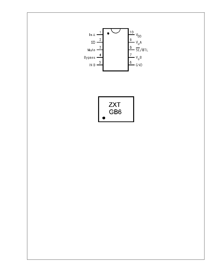
LM4919
1.5V, Mono 85mW BTL Output, 14mW Stereo Headphone
Audio Amplifier
General Description
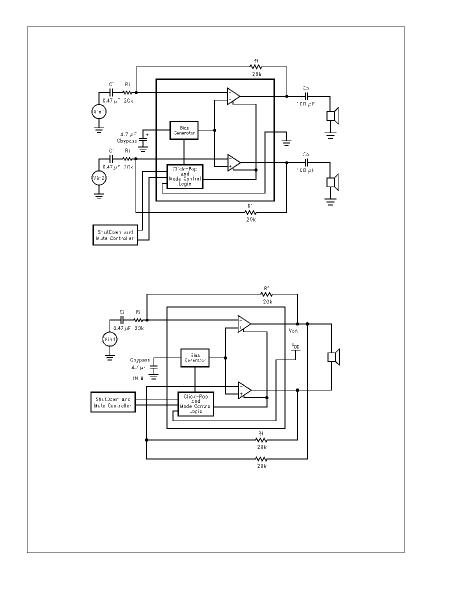
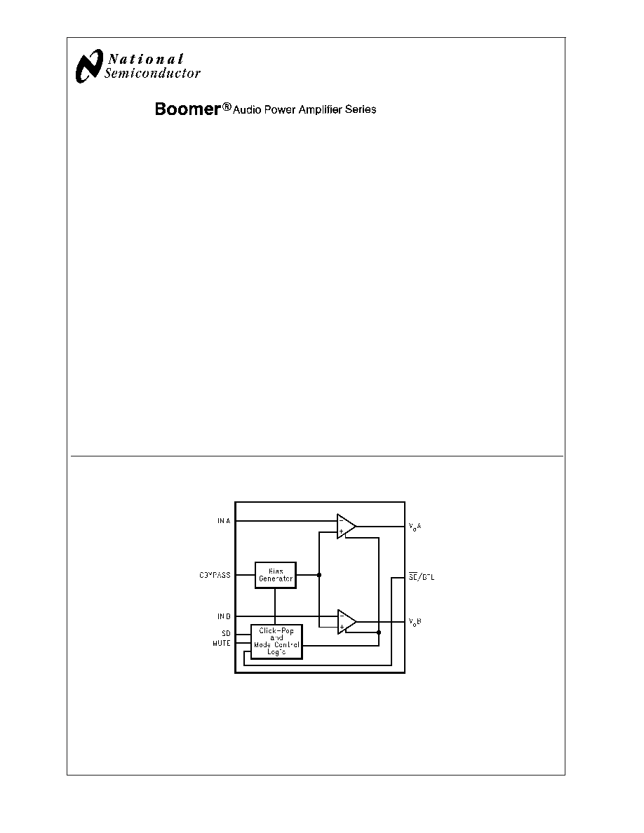
The unity gain stable LM4919 is both a mono-BTL audio
power amplifier and a Single Ended (SE) stereo headphone
amplifier. Operating on a single 1.5V supply, the mono BTL
mode delivers 85mW into an 8
load at 1% THD+N. In
Single Ended stereo headphone mode, the amplifier delivers
14mW per channel into a 16
load at 1% THD+N.
With the LM4919 packaged in the MM package, the cus-
tomer benefits include low profile and small size. This pack-
age minimizes PCB area and maximizes output power.
The LM4919 features circuitry that reduces output transients
("clicks" and "pops") during device turn-on and turn-off, an
externally controlled, low-power consumption, active-low
shutdown mode, and thermal shutdown. Boomer audio
power amplifiers are designed specifically to use few exter-
nal components and provide high quality output power in a
surface mount package.
Key Specifications
n
Mono-BTL output power
n
(R
L
= 8
, V
DD
= 1.5V, THD+N = 1%)
85mW (typ)
n
Stereo Headphone output power
n
(R
L
= 16
, V
DD
= 1.5V, THD+N = 1%)
14mW (typ)
n
Micropower shutdown current
0.02�A (typ)
n
Supply voltage operating range
0.9V
<
V
DD
<
2.5V
n
PSRR 1kHz, V
DD
= 1.5V, R
L
= 16
72dB (typ)
Features
n
Single-cell 0.9V to 2.5V battery operation
n
BTL mode for mono speaker
n
Single ended headphone operation with coupling
capacitors
n
Unity-gain stable
n
"Click and pop" suppression circuitry
n
Active low micropower shutdown
n
Low current, active-low mute mode
n
Thermal shutdown protection circuitry
Applications
n
Portable one-cell audio products
n
Portable one-cell electronic devices
Typical Application
Boomer
�
is a registered trademark of National Semiconductor Corporation.
20082101
FIGURE 1. Block Diagram
May 2004
LM4919
1.5V
,
Mono
85mW
BTL
Output,
14mW
Stereo
Headphone
Audio
Amplifier
� 2004 National Semiconductor Corporation
DS200821
www.national.com
Absolute Maximum Ratings
(Note 1)
If Military/Aerospace specified devices are required,
please contact the National Semiconductor Sales Office/
Distributors for availability and specifications.
Supply Voltage
3.6V
Storage Temperature
-65�C to +150�C
Input Voltage
-0.3V to V
DD
+0.3V
Power Dissipation (Note 2)
Internally limited
ESD Susceptibility(Note 3)
2000V
ESD Susceptibility (Note 4)
200V
Junction Temperature
150�C
Thermal Resistance
JA
(typ) MUB10A
175�C/W
Operating Ratings
Temperature Range
T
MIN
T
A
T
MAX
-40�C
T
A
85�C
Supply Voltage
0.9V
V
DD
2.5V
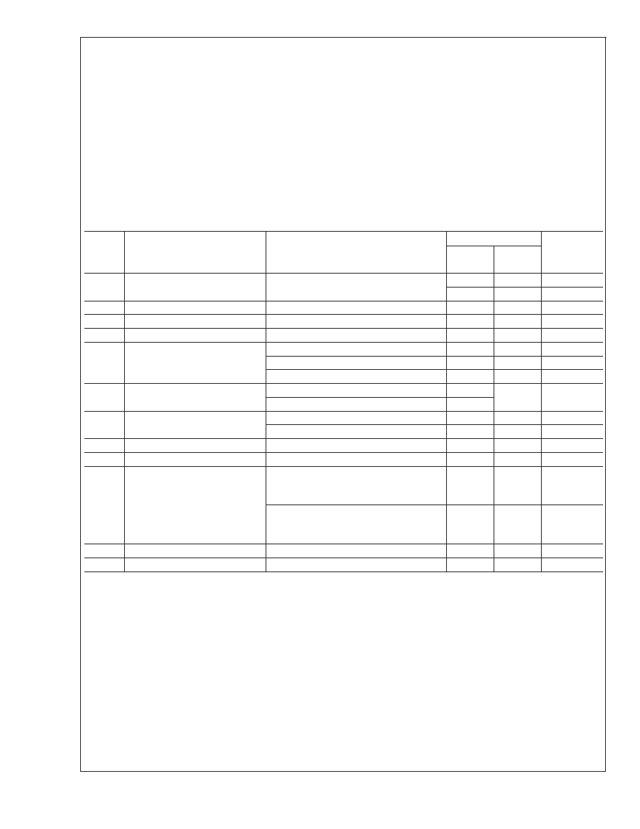
Electrical Characteristics for the LM4919
(Notes 1, 5)
The following specifications apply for the circuit shown in Figure 4 operating with V
DD
= 1. 5V, unless otherwise
specified. Limits apply for T
A
= 25�C.
Symbol
Parameter
Conditions
LM4919
Units
(Limits)
Typical
Limit
(Note 6)
(Note 7)
V
DD
Supply Voltage (Notes 10, 11)
0.9
V (min)
2.5
V (max)
I
DD
Quiescent Power Supply Current
V
IN
= 0V, I
O
= 0A, R
L
=
(Note 8)
0.9
1.4
mA (max)
I
SD
Shutdown Current
V
SHUTDOWN
= GND
0.02
�A
V
OS
Output Offset Voltage
BTL
5
50
mV (max)
P
O
Output Power (Note 9)
f = 1kHz
R
L
= 8
BTL, THD+N = 1%
85
70
mW (min)
R
L
= 16
SE, THD+N = 1%
14
mW (min)
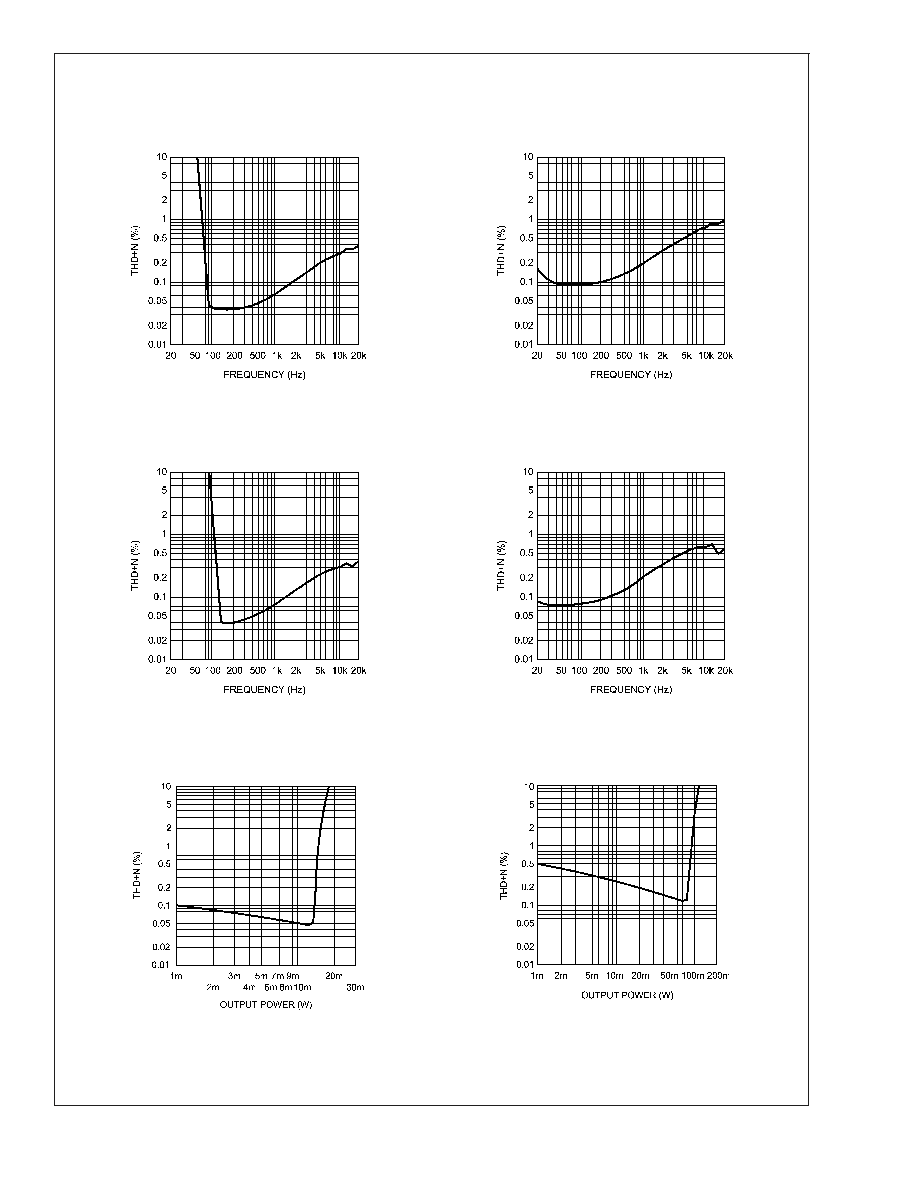
THD+N
Total Harmonic Distortion + Noise
R
L
= 8
, BTL, P
O
= 25mW, f = 1kHz
0.2
0.5
% (max)
R
L
= 16
, SE, P
O
= 5mW, f = 1kHz
0.07
V
NO
Output Voltage Noise
20Hz to 20kHz, A-weighted SE
10
�V
RMS
20Hz to 20kHz, A-weighted BTL
15
�V
RMS
I
MUTE
Mute Current
V
MUTE
= 0, SE
15
�A
Crosstalk
R
L
= 16
, SE
55
dB
PSRR
Power Supply Rejection Ratio
V
RIPPLE
= 200mV
P-P
C
BYPASS
= 4.7�F, R
L
= 8
f = 1kHz, BTL
70
dB
V
RIPPLE
= 200mV
P-P
sine wave
C
BYPASS
= 4.7�F, R
L
= 16
f = 1kHz, SE
72
dB
V
IH
Control Logic High
0.9
V
V
IL
Control Logic Low
0.3
V
Note 1: Absolute Maximum Ratings indicate limits beyond which damage to the device may occur. Operating Ratings indicate conditions for which the device is
functional, but do not guarantee specific performance limits. Electrical Characteristics state DC and AC electrical specifications under particular test conditions which
guarantee specific performance limits. This assumes that the device is within the Operating Ratings. Specifications are not guaranteed for parameters where no limit
is given, however, the typical value is a good indication of device performance.
Note 2: The maximum power dissipation is dictated by T
JMAX
,
JA
, and the ambient temperature T
A
and must be derated at elevated temperatures. The maximum
allowable power dissipation is P
DMAX
= (T
JMAX
- T
A
)/
JA
. For the LM4919, T
JMAX
= 150�C. For the
JA
s, please see the Application Information section or the
Absolute Maximum Ratings section.
Note 3: Human body model, 100pF discharged through a 1.5k
resistor.
Note 4: Machine model, 220pF�240pF discharged through all pins.
Note 5: All voltages are measured with respect to the ground (GND) pins unless otherwise specified.
Note 6: Typicals are measured at 25�C and represent the parametric norm.
Note 7: Datasheet min/max specification limits are guaranteed by design, test, or statistical analysis.
Note 8: The quiescent power supply current depends on the offset voltage when a practical load is connected to the amplifier.
Note 9: Output power is measured at the device terminals.
LM4919
www.national.com
4