LM4926
Ground-Referenced, Ultra Low Noise, Fixed Gain, 80mW
Stereo Headphone Amplifier
General Description
The LM4926 is a ground referenced, fixed-gain audio power
amplifier capable of delivering 80mW of continuous average
power into a 16
single-ended load with less than 1%
THD+N from a 3V power supply.
The LM4926 features a new circuit technology that utilizes a
charge pump to generate a negative reference voltage. This
allows the outputs to be biased about ground, thereby elimi-
nating output-coupling capacitors typically used with normal
single-ended loads.
The LM4926 features an Automatic Standby Mode circuitry
(patent pending). In the absence of an input signal, after
approximately 12 seconds, the LM4926 goes into low cur-
rent standby mode. The LM4926 recovers into full power
operating mode immediately after a signal is applied to either
the left or right input pins. This feature saves power supply
current in battery operated applications.
Boomer audio power amplifiers were designed specifically to
provide high quality output power with a minimal amount of
external components. The LM4926 does not require output
coupling capacitors or bootstrap capacitors, and therefore is
ideally suited for mobile phone and other low voltage appli-
cations where minimal power consumption is a primary re-
quirement.
The LM4926 features a low-power consumption shutdown
mode selectable for either channel separately. This is ac-
complished by driving either the SD_RC (Shutdown Right
Channel) or SD_LC (Shutdown Left Channel) (or both) pins
with logic low, depending on which channel is desired shut-
down. Additionally, the LM4926 features an internal thermal
shutdown protection mechanism.
The LM4926 contains advanced pop & click circuitry that
eliminates noises which would otherwise occur during
turn-on and turn-off transitions.
The LM4926 has an internal fixed gain of 1.5V/V.
Key Specifications
j
Improved PSRR at 217Hz
70dB (typ)
j
Power Output at V
DD
= 3V,
R
L
= 16
, THD % 1%
80mW (typ)
j
Shutdown Current
0.01�A (typ)
j
Internal Fixed Gain
1.5V/V (typ)
j
Operating Voltage
1.6V to 4.2V
Features
n
Ground referenced outputs
n
High PSRR
n
Available in space-saving micro SMD package
n
Ultra low current shutdown mode
n
Improved pop & click circuitry eliminates noises during
turn-on and turn-off transitions
n
No output coupling capacitors, snubber networks,
bootstrap capacitors, or gain-setting resistors required
n
Shutdown either channel independently
Applications
n
Notebook PCs
n
Mobile Phone
n
PDAs
n
Portable electronic devices
n
MP3 Players
Boomer
�
is a registered trademark of National Semiconductor Corporation.
June 2005
LM4926
Ground-Referenced,
Ultra
Low
Noise,
Fixed
Gain,
80mW
Stereo
Headphone
Amplifier
� 2005 National Semiconductor Corporation
DS201161
www.national.com

Typical Application
201161B8
FIGURE 1. Typical Audio Amplifier Application Circuit
LM4926
www.national.com
2
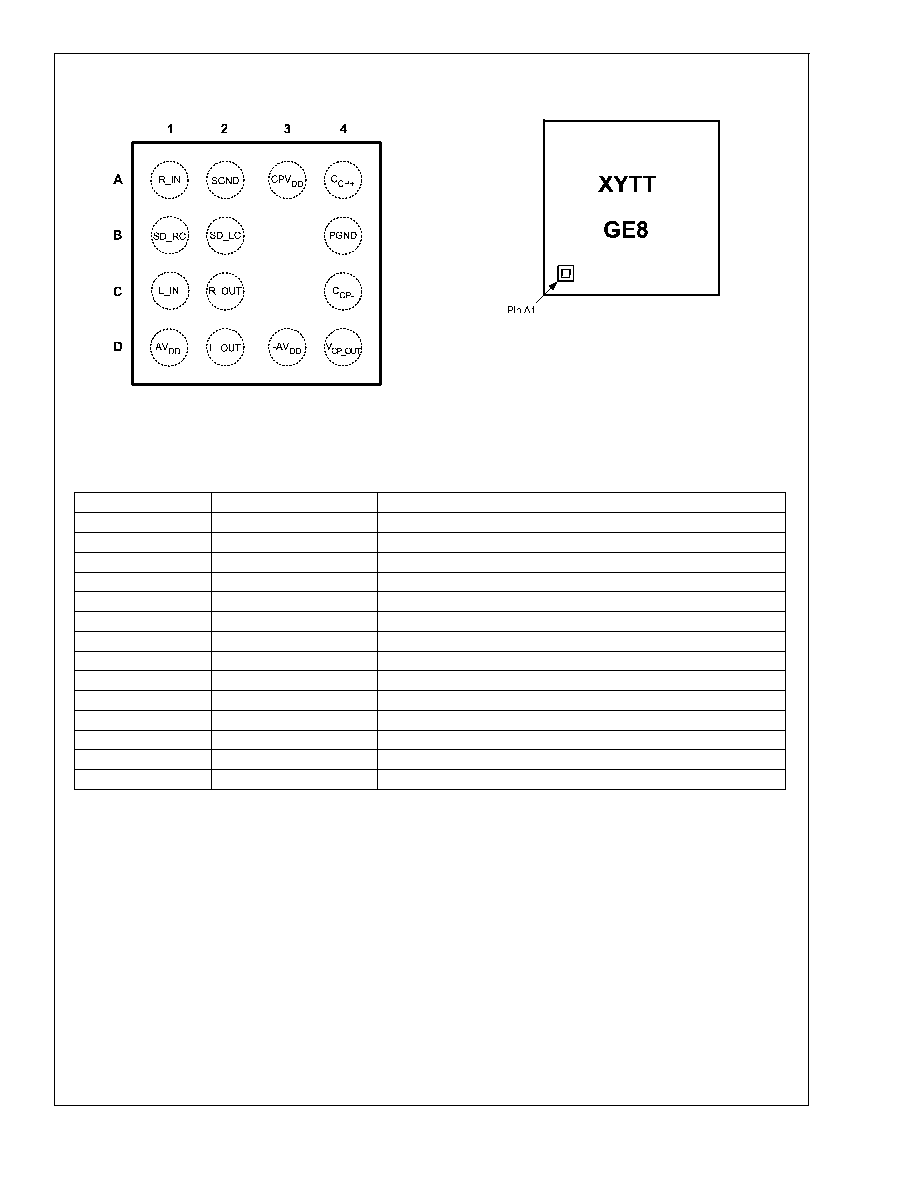
Connection Diagrams
microSMD Package
16 � Bump TL Marking
20116109
Top View
Order Number LM4926TL
See NS Package Number TLE1411A
20116178
Top View
XY � Date Code
TT � Lot Traceability
G � Boomer Family
E8 � LM4926TL
Pin Descriptions
Pin
Name
Function
A1
R_IN
Right Channel Input
A2
SGND
Signal Ground
A3
CPV
DD
Charge Pump Power Supply
A4
C
CP+
Positive Terminal - Charge Pump Flying Capacitor
B1
SD_RC
Active-Low Shutdown, Right Channel
B2
SD_LC
Active-Low Shutdown, Left Channel
B4
PGND
Power Ground
C1
L_IN
Left Channel Input
C2
R_OUT
Right Channel Input
C4
C
CP-
Negative Terminal - Charge Pump Flying Capacitor
D1
+AV
DD
Positive Power Supply - Amplifier
D2
L_OUT
Left Channel Output
D3
-AV
DD
Negative Power Supply - Amplifier
D4
V
CP_OUT
Charge Pump Power Output
LM4926
www.national.com
3
Absolute Maximum Ratings
(Note 2)
If Military/Aerospace specified devices are required,
please contact the National Semiconductor Sales Office/
Distributors for availability and specifications.
Supply Voltage
4.5V
Storage Temperature
-65�C to +150�C
Input Voltage
-0.3V to V
DD
+ 0.3V
Power Dissipation (Note 3)
Internally Limited
ESD Susceptibility (Note 4)
2000V
ESD Susceptibility (Note 5)
200V
Junction Temperature
150�C
Thermal Resistance
JA
(typ) TLE1411A (Note 11)
86�C/W
Operating Ratings
Temperature Range
T
MIN
T
A
T
MAX
-40�C
T
A
85�C
Supply Voltage (V
DD
)
1.6V
V
DD
4.2V
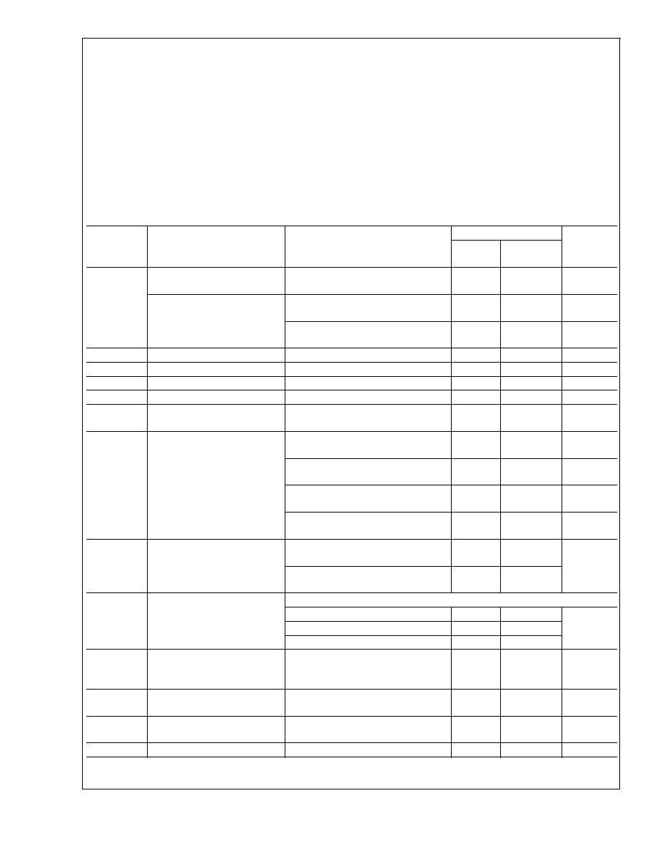
Electrical Characteristics V
DD
= 3V
(Note 1)
The following specifications apply for V
DD
= 3V and 16
load unless otherwise specified. Limits apply to T
A
= 25�C.
Symbol
Parameter
Conditions
LM4926
Units
(Limits)
Typ
(Note 6)
Limit
(Notes 7, 8)
I
DD
Quiescent Power Supply Current
Auto Standby Mode
V
IN
= 0V, inputs terminated
both channels enabled
2.3
mA
Quiescent Power Supply Current
Full Power Mode
V
IN
= 0V, inputs terminated
both channels enabled
7
10
mA (max)
V
IN
= 0V, inputs terminated
one channel enabled
5
mA
I
SD
Shutdown Current
V
SD_LC
= V
SD_RC
= GND
0.1
1.8
�A (max)
V
OS
Output Offset Voltage
R
L
= 32
, V
IN
= 0V
0.7
5
mV (max)
A
V
Voltage Gain
�1.5
V/V
A
V
Gain Match
1
%
R
IN
Input Resistance
20
15
25
k
(min)
k
(max)
P
O
Output Power
THD+N = 1% (max); f = 1kHz,
R
L
= 16
, one channel
80
mW
THD+N = 1% (max); f = 1kHz,
R
L
= 32
, one channel
65
mW
THD+N = 1% (max); f = 1kHz,
R
L
= 16
, (two channels in phase)
43
38
mW (min)
THD+N = 1% (max); f = 1kHz,
R
L
= 32
, (two channels in phase)
50
45
mW (min)
THD+N
Total Harmonic Distortion +
Noise
P
O
= 60mW, f = 1kHz, R
L
= 16
single channel
0.04
%
P
O
= 50mW, f = 1kHz, R
L
= 32
single channel
0.03
PSRR
Power Supply Rejection Ratio
Full Power Mode
V
RIPPLE
= 200mVp-p, Input Referred
f = 217Hz
70
dB
f = 1kHz
65
f = 20kHz
50
SNR
Signal-to-Noise Ratio
R
L
= 32
, P
OUT
= 20mW,
(A-weighted)
f = 1kHz, BW = 20Hz to 22kHz
100
dB
V
IH
Shutdown Input Voltage High
V
IH
=
0.7*CPV
DD
V
V
IL
Shutdown Input Voltage Low
V
IL
=
0.3*CPV
DD
V
T
WU
Wake Up Time From Shutdown
5
�s
LM4926
www.national.com
4
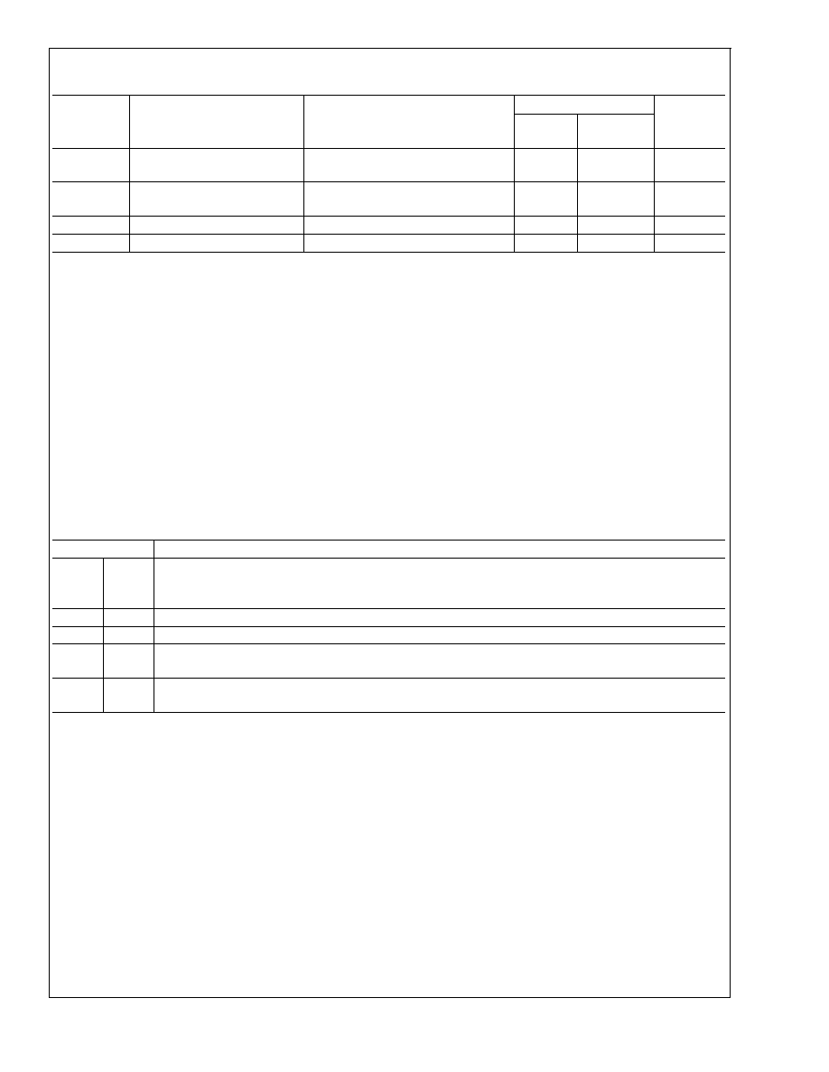
Electrical Characteristics V
DD
= 3V
(Note 1) (Continued)
The following specifications apply for V
DD
= 3V and 16
load unless otherwise specified. Limits apply to T
A
= 25�C.
Symbol
Parameter
Conditions
LM4926
Units
(Limits)
Typ
(Note 6)
Limit
(Notes 7, 8)
X
TALK
Crosstalk
R
L
= 16
, P
O
= 1.6mW,
f = 1kHz
60
dB
Z
OUT
Output Impedance
Input Terminated
Input not terminated
60
k
I
L
Input Leakage
�
0.1
nA
V
IN THRESH
Input Voltage Threshold
2.8
mVp
Note 1: All voltages are measured with respect to the GND pin unless otherwise specified.
Note 2: Absolute Maximum Ratings indicate limits beyond which damage to the device may occur. Operating Ratings indicate conditions for which the device is
functional but do not guarantee specific performance limits. Electrical Characteristics state DC and AC electrical specifications under particular test conditions that
guarantee specific performance limits. This assumes that the device is within the Operating Ratings. Specifications are not guaranteed for parameters where no limit
is given; however, the typical value is a good indication of device performance.
Note 3: The maximum power dissipation must be derated at elevated temperatures and is dictated by T
JMAX
,
JA
, and the ambient temperature, T
A
. The maximum
allowable power dissipation is P
DMAX
= (T
JMAX
- T
A
) /
JA
or the number given in Absolute Maximum Ratings, whichever is lower. For the LM4926, see power
de-rating currents for more information.
Note 4: Human body model, 100pF discharged through a 1.5k
resistor.
Note 5: Machine Model, 220pF - 240pF discharged through all pins.
Note 6: Typicals are measured at 25�C and represent the parametric norm.
Note 7: Limits are guaranteed to National's AOQL (Average Outgoing Quality Level).
Note 8: Datasheet min/max specification limits are guaranteed by design, test, or statistical analysis.
Note 9: If the product is in shutdown mode and V
DD
exceeds 4.2V (to a max of 4.5V V
DD
), then most of the excess current will flow through the ESD protection
circuits. If the source impedance limits the current to a max of 10mA, then the part will be protected. If the part is enabled when V
DD
is above 4.5V, circuit
performance will be curtailed or the part may be permanently damaged.
Note 10: Human body model, 100pF discharged through a 1.5k
resistor.
Note 11:
JA
value is measured with the device mounted on a PCB with a 3" x 1.5", 1oz copper heatsink.
External Components Description
(Figure 1)
Components
Functional Description
1.
C
i
Input coupling capacitor which blocks the DC voltage at the amplifier's input terminals. Also creates a
high-pass filter with R
i
at f
C
= 1/(2
R
i
C
i
). Refer to the section Proper Selection of External Components, for
an explanation of how to determine the value of C
i
.
2.
C
1
Flying capacitor. Low ESR ceramic capacitor (
100m)
3.
C
2
Output capacitor. Low ESR ceramic capacitor (
100m)
4.
C
3
Tantalum capacitor. Supply bypass capacitor which provides power supply filtering. Refer to the Power Supply
Bypassing section for information concerning proper placement and selection of the supply bypass capacitor.
5.
C
4
Ceramic capacitor. Supply bypass capacitor which provides power supply filtering. Refer to the Power Supply
Bypassing section for information concerning proper placement and selection of the supply bypass capacitor.
LM4926
www.national.com
5