LM4928
1.2 Watt Stereo Fully Differential Audio Amplifier with RF
Suppression and Shutdown Low
General Description
The LM4928 is an stereo fully differential stereo audio power
amplifier primarily designed for demanding applications in
mobile phones and other portable communication devices. It
is capable of delivering 1.2 watts of continuous average
power to a 8
load with less than 1% distortion (THD+N)
from a 5V
DC
power supply.
Boomer audio power amplifiers were designed specifically to
provide high quality output power with a minimal amount of
external components. The LM4928 does not require output
coupling capacitors or bootstrap capacitors, and therefore is
ideally suited for mobile phone and other low voltage appli-
cations where minimal power consumption is a primary re-
quirement.
The LM4928 features a low-power consumption shutdown
mode. To facilitate this, shutdown may be enabled by logic
low. Additionally, the LM4928 features an internal thermal
shutdown protection mechanism.
The LM4928 contains advanced pop & click circuitry which
eliminates noises which would otherwise occur during
turn-on and turn-off transitions.
Key Specifications
j
Improved PSRR at 217Hz
90dB (typ)
j
Output Power at 5.0V
@
1% THD+N (8
) 1.2W (typ)
j
Output Power at 3.0V
@
1% THD+N (8
)400mW (typ)
j
Shutdown Current
0.1�A (typ)
Features
n
RF Suppression Circuitry
n
Fully differential amplification
n
Available in space-saving micro SMD and LLP packages
n
Ultra low current shutdown mode
n
Can drive capacitive loads up to 100pF
n
Improved pop & click circuitry eliminates noises during
turn-on and turn-off transitions
n
2.4 - 5.5V operation
n
No output coupling capacitors, snubber networks or
bootstrap capacitors required
Applications
n
Mobile phones
n
PDAs
n
Portable electronic devices and accessories
Boomer
�
is a registered trademark of National Semiconductor Corporation.
February 2006
LM4928
1.2
W
att
Stereo
Fully
Differential
Audio
Power
Amplifier
with
RF
Suppression
and
Shutdown
Low
� 2006 National Semiconductor Corporation
DS201600
www.national.com
Absolute Maximum Ratings
(Note 2)
If Military/Aerospace specified devices are required,
please contact the National Semiconductor Sales Office/
Distributors for availability and specifications.
Supply Voltage
6.0V
Storage Temperature
-65�C to +150�C
Input Voltage
-0.3V to V
DD
+0.3V
Power Dissipation (Note 3)
Internally Limited
ESD Susceptibility (Note 4)
2000V
ESD Susceptibility (Note 5)
200V
Junction Temperature
150�C
Thermal Resistance
JA
(SD)
50�C/W
JA
(micro SMD)
74�C/W
Soldering Information
See AN-1187
Operating Ratings
Temperature Range
T
MIN
T
A
T
MAX
-40�C
T
A
85�C
Supply Voltage
2.4V
V
DD
5.5V
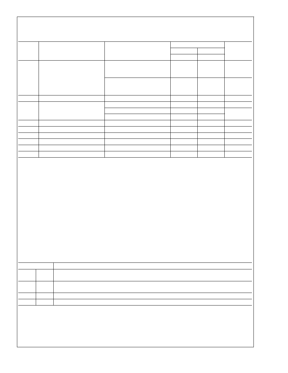
Electrical Characteristics V
DD
= 5V
(Notes 1, 2)
The following specifications apply for V
DD
= 5V, A
V
= 1, and 8
load unless otherwise specified. Limits apply for T
A
= 25�C.
Symbol
Parameter
Conditions
LM4928
Units
(Limits)
Typical
Limit
(Note 6)
(Note 7)
I
DD
Quiescent Power Supply Current
V
IN
= 0V, no load
V
IN
= 0V, R
L
= 8
(Both amplifiers)
4
4
7.5
mA (max)
I
SD
Shutdown Current
V
SHUTDOWN
= GND
(Both amplifiers)
0.1
1.0
�A (max)
P
o
Output Power
THD = 1% (max); f = 1 kHz
LM4928SD, R
L
= 4
(Note 9)
R
L
= 8
1.8
1.2
1.0
W
THD = 10% (max); f = 1 kHz
LM4928SD, R
L
= 4
(Note 9)
R
L
= 8
2.2
1.5
W
THD+N
Total Harmonic Distortion + Noise
P
o
= 1 Wrms; f = 1kHz
0.04
%
PSRR
Power Supply Rejection Ratio
V
ripple
= 200mV sine p-p
f = 217Hz (Note 8)
90
dB
f = 1kHz (Note 8)
90
CMRR
Common-Mode Rejection Ratio
f = 217Hz, V
CM
= 200mV
pp
70
50
dB (min)
V
OS
Output Offset
V
IN
= 0V
4
18
mV (max)
V
SDIH
Shutdown Voltage Input High
1.4
V
V
SDIL
Shutdown Voltage Input Low
0.4
V
SNR
Signal-to-Noise Ratio
P
O
= 1W, f = 1kHz
105
dB
T
WU
Wake-up time from Shutdown
Cbypass = 1�F
13
ms
Electrical Characteristics V
DD
= 3V
(Notes 1, 2)
The following specifications apply for V
DD
= 3V, A
V
= 1, and 8
load unless otherwise specified. Limits apply for T
A
= 25�C.
Symbol
Parameter
Conditions
LM4928
Units
(Limits)
Typical
Limit
(Note 6)
(Note 7)
I
DD
Quiescent Power Supply Current
V
IN
= 0V, no load
V
IN
= 0V, R
L
= 8
(Both amplifiers)
3.5
3.5
mA
I
SD
Shutdown Current
V
SHUTDOWN
= GND
(Both amplifiers)
0.1
1
�A (max)
LM4928
www.national.com
4
Electrical Characteristics V
DD
= 3V
(Notes 1, 2)
The following specifications apply for V
DD
= 3V, A
V
= 1, and 8
load unless otherwise specified. Limits apply for T
A
=
25�C. (Continued)
Symbol
Parameter
Conditions
LM4928
Units
(Limits)
Typical
Limit
(Note 6)
(Note 7)
P
o
Output Power
THD = 1% (max); f = 1 kHz
R
L
= 4
R
L
= 8
0.55
0.40
W
THD = 10% (max); f = 1 kHz
R
L
= 4
R
L
= 8
0.68
0.50
W
THD+N
Total Harmonic Distortion + Noise
P
o
= 0.25Wrms; f = 1kHz
0.05
%
PSRR
Power Supply Rejection Ratio
V
ripple
= 200mV sine p-p
f = 217Hz (Note 8)
90
dB
f = 1kHz (Note 8)
90
CMRR
Common-Mode Rejection Ratio
f = 217Hz, V
CM
= 200mV
pp
70
50
dB (min)
V
OS
Output Offset
V
IN
= 0V
4
18
mV (max)
V
SDIH
Shutdown Voltage Input High
1.4
V
V
SDIL
Shutdown Voltage Input Low
0.4
V
SNR
Signal-to-Noise Ratio
P
O
= 0.4W, f = 1kHz
105
dB
T
WU
Wake-up time from Shutdown
Cbypass = 1�F
9
ms
Note 1: All voltages are measured with respect to the ground pin, unless otherwise specified.
Note 2: Absolute Maximum Ratings indicate limits beyond which damage to the device may occur. Operating Ratings indicate conditions for which the device is
functional, but do not guarantee specific performance limits. Electrical Characteristics state DC and AC electrical specifications under particular test conditions which
guarantee specific performance limits. This assumes that the device is within the Operating Ratings. Specifications are not guaranteed for parameters where no limit
is given, however, the typical value is a good indication of device performance.
Note 3: The maximum power dissipation must be derated at elevated temperatures and is dictated by T
JMAX
,
JA
, and the ambient temperature T
A
. The maximum
allowable power dissipation is P
DMAX
= (T
JMAX
� T
A
) /
JA
or the number given in Absolute Maximum Ratings, whichever is lower. For the LM4928, see power
derating curve for additional information.
Note 4: Human body model, 100pF discharged through a 1.5k
resistor.
Note 5: Machine Model, 220pF � 240pF discharged through all pins.
Note 6: Typicals are measured at 25�C and represent the parametric norm.
Note 7: Limits are guaranteed to National's AOQL (Average Outgoing Quality Level).
Note 8: Inputs are AC terminated to GND.
Note 9: When driving 4
loads from a 5V power supply, the LM4928SD must be mounted to a circuit board with the exposed-DAP area soldered down to at least
4in
2
plane of 1oz, copper.
Note 10: Data taken with BW = 80kHz and A
V
= 1 except where specified.
Note 11: Maximum Power Dissipation (P
DMAX
) in the device occurs at an output power level significantly below full output power. P
DMAX
can be calculated using
Equation 4 shown in the Application section. It may also be obtained from the Power Dissipation graphs.
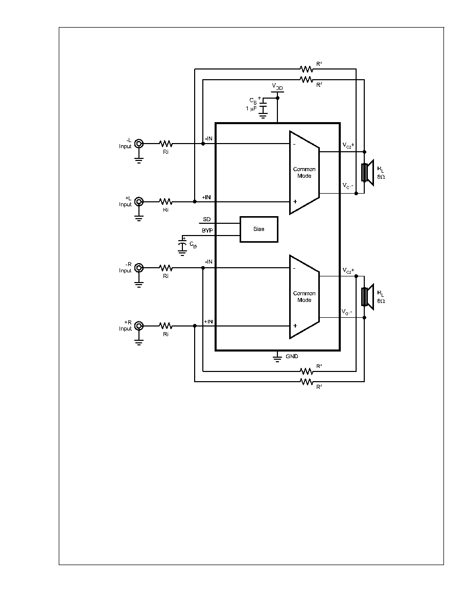
External Components Description
(Figure 1)
Components
Functional Description
1.
C
S
Supply bypass capacitor which provides power supply filtering. Refer to the Power Supply Bypassing
section for information concerning proper placement and selection of the supply bypass capacitor.
2.
C
B
Bypass pin capacitor which provides half-supply filtering. Refer to the Power Supply Bypassing section for
information concerning proper placement and selection of C
B
.
3.
R
i
Inverting input resistance which sets the closed-loop gain in conjunction with R
f
.
4.
R
f
External feedback resistance which sets the closed-loop gain in conjunction with R
i
.
LM4928
www.national.com
5