LM4931
Audio Subsystem with Mono High Efficiency
Loudspeaker and Stereo Headphone Amplifiers
General Description
The LM4931 is an integrated audio subsystem that supports
voice and digital audio functions. The LM4931 includes a
high quality stereo DAC, voice band codec, a stereo head-
phone amplifier and a high-power high efficiency mono
speaker amplifier. It is primarily designed for demanding
applications in mobile phones and other portable devices.
The LM4931 features an I
2
S serial interface for full range
audio, a 16-bit PCM bi-directional serial interface for the
voice band codec and an I
2
C/SPI compatible interface for
control. The full range music path features an SNR of 86dB
with an 18-bit 48kHz input. The headphone amplifier delivers
at least 26mW
RMS
to a 32
single-ended stereo load with
less than 1% distortion (THD+N) when AV
DD
= 3.3V
DC
. The
mono speaker amplifier delivers up to 570mW
RMS
into an 8
load with less than 1% distortion when AV
DD
= 3.3V
DC
.
The LM4931 employs advanced techniques to reduce power
consumption, to reduce controller overhead, and to eliminate
click and pop. Boomer audio power amplifiers were de-
signed specifically to provide high quality output power with
a minimal amount of external components. It is therefore
ideally suited for mobile phone and other low voltage appli-
cations where minimal power consumption, PCB area, and
cost are primary requirements.
Key Specifications
j
P
LS OUT
at AV
DD
= 5V, 8
1% THD+N
1.1W (typ)
j
P
LS OUT
at AV
DD
= 3.3V, 8
1% THD+N
570mW (typ)
j
P
H/P OUT
at AV
DD
= 5V & AV
DD
= 3.3V, 32
1% THD+N
26mW (typ)
j
Supply voltage range
DV
DD
2.7V to 4.0V
AV
DD
(Note 8)
2.7V to 5.0V
j
Shutdown current
1.1µA (typ)
j
PSRR at 217Hz, AV
DD
= 3V
62dB (typ)
j
SNR (Voice Codec)
75dB (typ)
j
SNR (Audio DAC)
86dB (typ)
Features
n
18-bit 44.1kHz or 48kHz stereo DAC
n
16-bit 8kHz , 12kHz , 16kHz, or 24kHz voice-band
codec
n
PLL for operation from common system clocks
n
Either I
2
C or SPI compatible serial interface
n
I
2
S digital audio data serial interface
n
PCM voice audio data serial interface
n
Differential analog microphone input
n
26mW/channel stereo headphone amplifier
n
570mW mono high efficiency BTL 8
amplifier
n
32-step volume control for audio output amplifiers with
1.5dB step size.
n
Unity-gain stable headphone amplifiers
n
No snubber networks or bootstrap capacitors are
required by the headphone or hands-free amplifiers
n
Adjustable digital side-tone attenuation
n
16-step volume control for microphone preamp with 2dB
step size
n
Configurable GPIO/Status Port
n
Available in the 42 bump micro-SMD package
Applications
n
2.5 and 3G Mobile Phones and Multimedia Terminals
n
PDAs, Internet Appliances and Portable Gaming
n
Portable DVD/CD/AAC/MP3 Players
n
Digital Cameras and Toys
Boomer
Æ
is a registered trademark of National Semiconductor Corporation.
June 2004
LM4931
Audio
Subsystem
with
Mono
High
Efficiency
Loudspeaker
and
Stereo
Headphone
Amplifiers
© 2004 National Semiconductor Corporation
DS201009
www.national.com
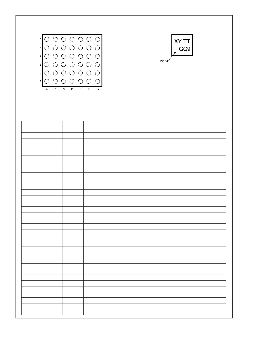
Connection Diagrams
42-Bump micro SMD
42-Bump micro SMD Marking
20100958
Top View (Bump Side Down)
Order Number LM4931ITL
See NS Package Number TLA42YVA
201009I7
Top View
XY - Date Code
TT - Die Tracebility
G - Boomer Family
C9 - LM4931ITL
Pin Descriptions
PIN
PIN NAME
D/A
I/O
DESCRIPTION
A1
MIC_P
A
I
Microphone positive differential input
A2
MIC_N
A
I
Microphone negative differential input
A3
VDD(MIC)
A
I
Analog Vdd for microphone section
A4
MODE
D
I
Selects between SPI and I
2
C control interfaces (I
2
C = 0, SPI = 1)
A5
SDA/SDI
D
I/O
I
2
C_SDA or SPI_SDI depending on the MODE control
A6
NC
N/A
N/A
No Connect
B1
MIC_P
A
I
Microphone positive differential input
B2
MIC_BIAS
A
O
2V ultra clean power supply for microphones
B3
BYPASS
A
I
Click and Pop / VDD/2 reference filter
B4
ADDR/ENB
D
I
I
2
C_ADDR or SPI_ENB depending on the MODE control
B5
SCL/SCK
D
I
I
2
C_SCL or SPI_SCK depending on the MODE control
B6
PCM_SDI
D
I
PCM_SDI voice data input
C1
VSS(MIC)
A
I
Analog Vss for microphone section
C2
MIC_REF
A
I
Filter for microphone power supply
C3
NC
N/A
N/A
No Connect
C4
PCM_SDO
D
O
PCM_SDO serial data output
C5
PCM_SYNC
D
I/O
PCM_SYNC pulse for the PCM bus
C6
PCM-CLK
D
I/O
PCM_SYNC pulse for the PCM bus
D1
HPL
A
O
Left Headphone output
D2
VSS(HP)
A
I
Analog Vss for Headphone and Mixer sections
D3
VSS(HP)
A
I
Analog Vss for Headphone and Mixer sections
D4
I
2
S_SDI
D
I
I
2
S serial data input
D5
I
2
S_CLK
D
I/O
I
2
S clock signal
D6
VSSD
D
I
Digital Vss
E1
VDD(HP)
A
I
Analog Vdd for Headphone and Mixer sections
E2
HPR
A
O
Right Headphone output
E3
GPIO
D
O
Configurable multi purpose output
E4
I
2
S_WS
D
I/O
I
2
S word select signal
E5
MCLK
D
I
Input clock from 10MHz - 24.576MHz
E6
VDDD
D
I
Digital Vdd
F1
LS+
A
O
Loudspeaker positive output
F2
VDD(LS)
A
I
Analog Vdd for Loudspeaker section
F3
HP_SENSE
A
I
Input for headphone connection sense circuit
LM4931
www.national.com
3
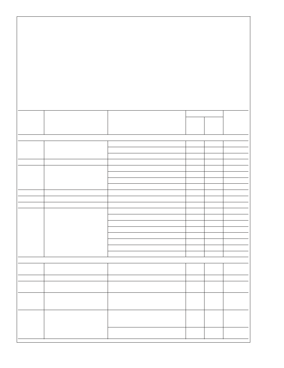
Absolute Maximum Ratings
(Notes 1, 2)
If Military/Aerospace specified devices are required,
please contact the National Semiconductor Sales Office/
Distributors for availability and specifications.
Analog Supply Voltage
6.0V
Digital Supply Voltage
6.0V
Storage Temperature
-65∞C to +150∞C
Power Dissipation (Note 3)
Internally Limited
ESD Susceptibility
Human Body Model (Note 4)
2500V
Machine Model (Note 5)
200V
Junction Temperature
150∞C
Thermal Resistance
JA
- TLA42YVA
105∞C/W
Operating Ratings
Temperature Range
T
MIN
T
A
T
MAX
-40∞C
T
A
+85∞C
Supply Voltage
DV
DD
(Note 8)
2.7V - 4.0V
AV
DD
(Note 8)
2.7V - 5.0V
Electrical Characteristics DV
DD
= 3V, AV
DD
= 3V, R
LHP
= 32
, R
LHF
= 8
(Notes 1, 2)
The following specifications apply for the circuit shown in Figure 1, unless otherwise specified. Limits apply for T
A
= 25∞C.
Symbol
Parameter
Conditions
LM4931
Units
(Limits)
Typical
(Note 6)
Limits
(Note 7)
Power
DI
SD
Digital Shutdown Current
Mode 0
f
MLCK
= 12MHz (Note 9)
400
500
µA (max)
No MCLK
1
2
µA (max)
DI
ST
Digital Standby Current
Mode 1, f
MCLK
= 12MHz
400
1200
µA (max)
f
MLCK
= 12MHz
DI
DD
Digital Power Supply Current
Mode 2, 3, 4
1.3
3.2
mA (max)
Mode 5, 6, 7
2.8
7
mA (max)
Mode 8, 9, 10
3.2
7.5
mA (max)
PLLI
DD
PLL Quiescent Current
f
MCLK
= 12MHz
2.8
3.5
mA (max)
AI
SD
Analog Shutdown Current
Mode 0, No load
0.1
2.5
µA (max)
AI
ST
Analog Standby Current
Mode 1, No load
100
200
µA (max)
AI
DD
Analog Power Supply Quiescent
Current
No Load
Mode 2
7.8
19
mA (max)
Mode 3
5.3
10
mA (max)
Mode 4
8.6
15
mA (max)
Mode 5
8.4
15
mA (max)
Mode 6
6.0
15
mA (max)
Mode 7
9.2
15
mA (max)
Mode 8, 9, 10
10.1
16
mA (max)
Loudspeaker Amplifier
V
FS
Full-Scale Output Voltage
Loudspeaker Amplifier)
8
load, 0dB gain setting
2.6
V
P-P
THD+N
Total Harmonic Distortion + Noise
f
OUT
= 1kHz, P
OUT
= 200mW
0.4
%
P
OLS
Loudspeaker Amplifier Output
Power
THD = 1% (max), f
OUT
= 1kHz
470
350
mW (min)
PSRR
Power Supply Rejection Ratio
(Loudspeaker Amplifier)
C
B
= 1.0µF
V
RIPPLE
= 200mV
P-P
f
RIPPLE
= 217Hz
54
dB
Signal = V
O
at 0dBFS, f = 1kHz,
Noise = digital zero, A-weighted,
0dB gain setting (Note 10)
SNR (Voice)
Signal-to-Noise Ratio of Voice
Channel (Loudspeaker Amplifier)
f
MCLK
= 12.288MHz, PLL disabled
71
dB
LM4931
www.national.com
5