LM4946
Output Capacitor-Less Audio Subsystem with
Programmable National 3D
General Description
The LM4946 is an audio power amplifier capable of deliver-
ing 540mW of continuous average power into a mono 8
bridged-tied load (BTL) with 1% THD+N, 35mW per channel
of continuous average power into stereo 32
single-ended
(SE) loads with 1% THD+N, or an output capacitor-less
(OCL) configuration with identical specifications as the SE
configuration, from a 3.3V power supply.
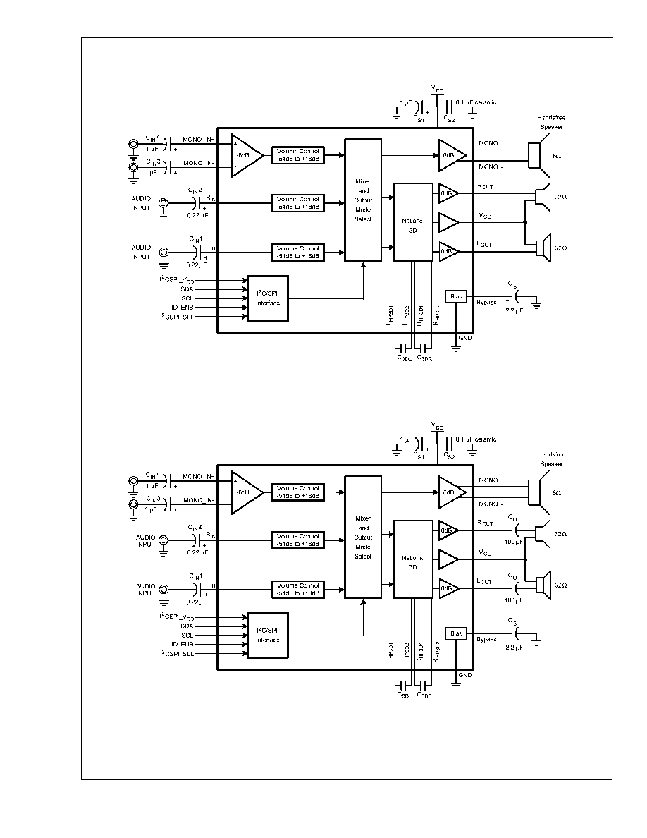
The LM4946 has three input channels: one pair for a two-
channel stereo signal and the third for a differential single-
channel mono input. The LM4946 features a 32-step digital
volume control and eight distinct output modes. The digital
volume control, 3D enhancement, and output modes (mono/
SE/OCL) are programmed through a two-wire I
2
C or a three-
wire SPI compatible interface that allows flexibility in routing
and mixing audio channels.
The LM4946 is designed for cellular phone, PDA, and other
portable handheld applications. It delivers high quality output
power from a surface-mount package and requires only
seven external components in the OCL mode (two additional
components in SE mode).
Key Specifications
j
THD+N at 1kHz, 540mW
into 8
BTL (3.3V)
1.0% (typ)
j
THD+N at 1kHz, 35mW
into 32
SE (3.3V)
1.0% (typ)
j
Single Supply Operation (V
DD
)
2.7 to 5.5V
j
I
2
C/SPI Single Supply Operation
2.2 to 5.5V
Features
n
I
2
C/SPI Control Interface
n
I
2
C/SPI programmable National 3D Audio
n
I
2
C/SPI controlled 32 step digital volume control (-54dB
to +18dB)
n
Three independent volume channels (Left, Right, Mono)
n
Eight distinct output modes
n
LLP surface mount packaging
n
"Click and Pop" suppression circuitry
n
Thermal shutdown protection
n
Low shutdown current (0.02uA, typ)
n
RF immunity topology
Applications
n
Mobile Phones
n
PDAs
Boomer
Æ
is a registered trademark of National Semiconductor Corporation.
May 2006
LM4946Output
Capacitor-Less
Audio
Subsystem
with
Programmable
National
3D
© 2006 National Semiconductor Corporation
DS201628
www.national.com

Connection Diagrams
24 Lead LLP Package
20162803
Top View
201628E8
Top View
U - Wafer Fab Code
Z - Assembly Plant Code
XY - Date Code
TT - Die Traceability
xxx - L4946SQ
Pin Descriptions
Pin Number
Name
Description
1
LHP3D2
Left Headphone Input 2
2
VOC
Center Amplifier Output
3
VDD
Power Supply
4
GND
Ground
5
ROUT
Right Headphone Output
6
LOUT
Left Headphone Output
7
I
2
CSPI_VDD
I
2
C or SPI Interface Power Supply
8
RIN
Right Input Channel
9
LIN
Left Input Channel
10
SDA
I
2
C/SPI Data
11
SCL
I
2
C/SPI Clock
12
GND
Ground
13
ID_ENB
I
2
Address Identification/SPI Enable Bar
14
I
2
CSPI_SEL
I
2
C or SPI Select
15
MONO+
Loudspeaker Output Positive
16
VDD
Power Supply
17
MONO-
Loudspeaker Output Negative
18
LHP3D1
Left Headphone 3D Input 1
19
RHP3D1
Right Headphone 3D Input 1
20
GND
Ground
21
BYPASS
Half-Supply Bypass
22
MONO_IN-
Loudspeaker Negative Input
23
MONO_IN+
Loudspeaker Positive Input
24
RHP3D2
Right Headphone 3D Input 2
LM4946
www.national.com
3

Absolute Maximum Ratings
(Note 2)
If Military/Aerospace specified devices are required,
please contact the National Semiconductor Sales Office/
Distributors for availability and specifications.
Supply Voltage
6.0V
Storage Temperature
-65∞C to +150∞C
Input Voltage
-0.3 to V
DD
+0.3
ESD Susceptibility (Note 3)
2.0kV
ESD Machine model (Note 6)
200V
Junction Temperature
150∞C
Solder Information (Note 1)
Vapor Phase (60 sec.)
215∞C
Infrared (15 sec.)
220∞C
Thermal Resistance (Note 8)
JA
(typ) - SQA24A
46∞C/W
Operating Ratings
Temperature Range
-40∞C to 85∞C
Supply Voltage (V
DD
)
2.7V
V
DD
5.5V
Supply Voltage (I
2
C/SPI)
2.2V
I
2
CSPI_V
DD
5.5V
Electrical Characteristics 3.3V
(Notes 2, 7)
The following specifications apply for V
DD
= 3.3V, T
A
= 25∞C, all volume controls set to 0dB, unless otherwise specified.
Symbol
Parameter
Conditions
LM4946
Units
(Limits)
Typical
(Note 4)
Limits
(Note 5)
I
DD
Supply Current
Output Modes 2, 4, 6
V
IN
= 0V; No load,
SE Headphone
3.25
mA
Output Modes 1, 3, 5, 7
V
IN
= 0V; No load,
SE Headphone
5.65
mA
Output Modes 2, 4, 6
V
IN
= 0V; No load,
OCL Headphone
4
6.5
mA (max)
Output Modes 1, 3, 5,
V
IN
= 0V; No load,
OCL Headphone
5
mA
Output Modes 7
V
IN
= 0V; No load,
OCL Headphone
6.5
10.5
mA (max)
I
SD
Shutdown Current
Output Mode 0
0.02
1
µA (max)
V
OS
Output Offset Voltage
V
IN
= 0V, Mode 7
Mono
12
50
mV (max)
V
IN
= 0V, Mode 7
Headphones
3
30
P
O
Output Power
MONO
OUT
; R
L
= 8
THD+N = 1%; f = 1kHz, BTL, Mode 1
540
500
mW (min)
R
OUT
and L
OUT
; R
L
= 32
THD+N = 1%; f = 1kHz, SE, Mode 4
35
30
mW (min)
THD+N
Total Harmonic Distortion + Noise
MONO
OUT
f = 1kHz
P
OUT
= 250mW; R
L
= 8
, BTL, Mode 1
0.05
%
R
OUT
and L
OUT
f = 1kHz
P
OUT
= 12mW; R
L
= 32
, SE, Mode 4
0.015
%
LM4946
www.national.com
4

Electrical Characteristics 3.3V
(Notes 2, 7) (Continued)
The following specifications apply for V
DD
= 3.3V, T
A
= 25∞C, all volume controls set to 0dB, unless otherwise specified.
Symbol
Parameter
Conditions
LM4946
Units
(Limits)
Typical
(Note 4)
Limits
(Note 5)
N
OUT
Output Noise
A-weighted,
inputs terminated to GND, output referred
Speaker; Mode 1
17
µV
Speaker; Mode 3, 7
27
µV
Speaker; Mode 5
33
µV
Headphone; SE, Mode 2
8
µV
Headphone; SE, Mode 4, 7
8
µV
Headphone; SE, Mode 6
12
µV
Headphone; OCL, Mode 2
8
µV
Headphone; OCL, Mode 4, 7
9
µV
Headphone; OCL, Mode 6
12
µV
PSRR
Power Supply Rejection Ratio
MONO
OUT
V
RIPPLE
= 200mV
PP
; f = 217Hz, R
L
= 8
C
B
= 2.2µF, BTL
All audio inputs terminated to GND;
output referred
BTL, Output Mode 1
76
dB
BTL, Output Mode 3, 7
65
dB
BTL, Output Mode 5
63
dB
Power Supply Rejection Ratio
R
OUT
and L
OUT
V
RIPPLE
= 200mV
PP
; f = 217Hz, R
L
= 32
C
B
= 2.2µF,
All audio inputs terminated to GND
output referred
SE, Output Mode 2
78
dB
SE, Output Mode 4,7
82
dB
SE, Output Mode 6
78
dB
OCL, Output Mode 2
84
dB
OCL, Output Mode 4, 7
78
dB
OCL, Output Mode 6
77
dB
Volume Control Step Size Error
±
0.2
dB
Digital Volume Control Range
Maximum attenuation
-54
≠56
≠52
dB (max)
dB (min)
Maximum gain
18
17.4
18.6
dB (min)
dB (max)
HP(SE) Mute Attenuation
Output Mode 1, 3, 5
96
dB
MONO_IN Input Impedance
R
IN
and L
IN
Input Impedance
Maximum gain setting
12.5
10
15
k
(min)
k
(max)
Maximum attenuation setting
110
90
130
k
(min)
k
(max)
CMRR
Common-Mode Rejection Ratio
f = 217Hz, V
CM
= 1Vpp,
Mode 1, BTL, R
L
= 8
61
dB
f = 217Hz, V
CM
= 1Vpp,
Mode 2, R
L
= 32
66
XTALK
Crosstalk
Headphone; P
O
= 12mW
f = 1kHz, OCL, mode 4
≠54
dB
Headphone; P
O
= 12mW
f = 1kHz, SE, mode 4
≠72
dB
T
WU
Wake-Up Time from Shutdown
C
B
= 2.2µF, OCL
100
ms
C
B
= 2.2µF, SE
135
ms
LM4946
www.national.com
5