LM4947
Mono Class D and Stereo Audio Subsystem with OCL
Headphone Amplifier and National 3D
General Description
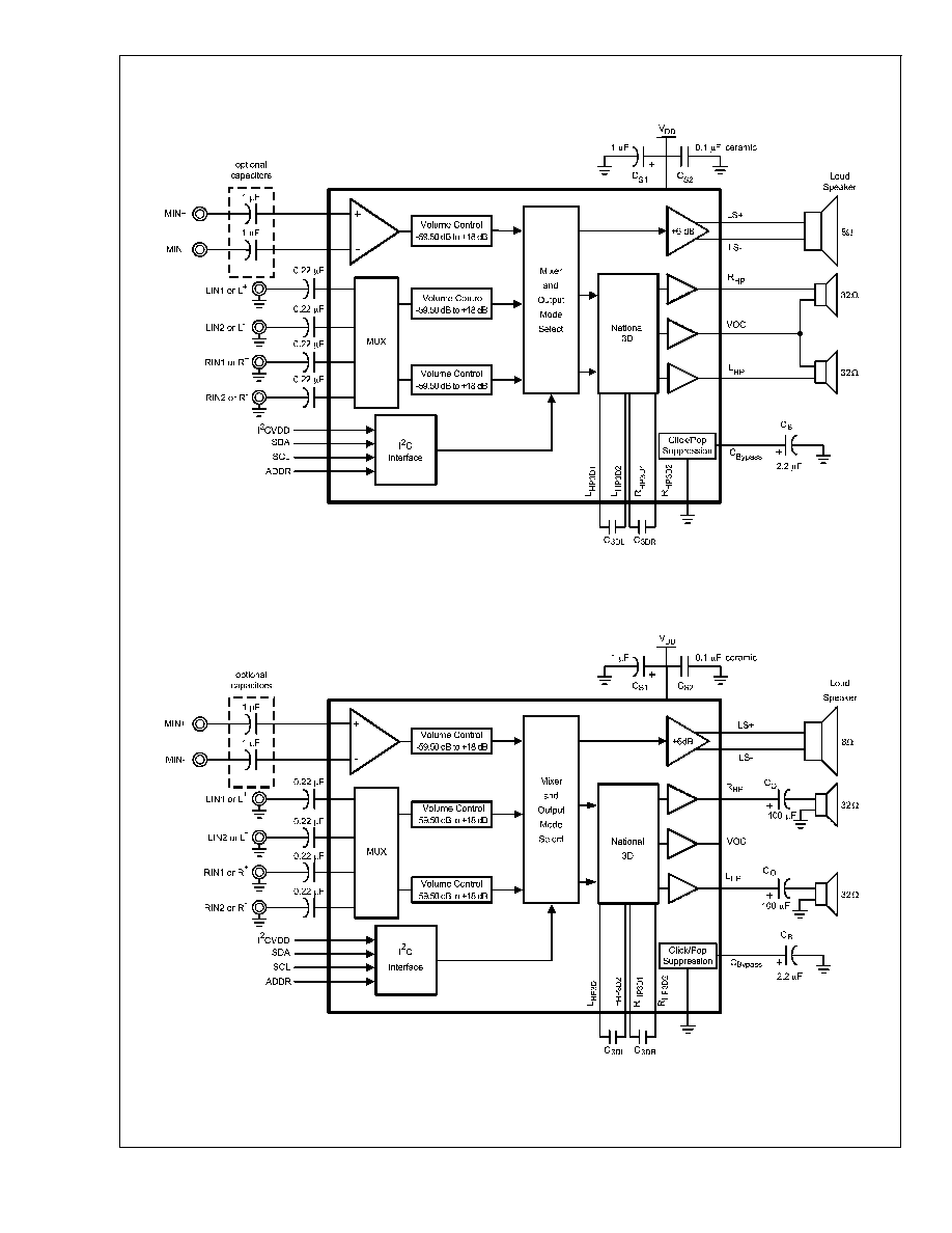
The LM4947 is an audio subsystem capable of efficiently
delivering 500mW (Class D operation) of continuous aver-
age power into a mono 8
bridged-tied load (BTL) with 1%
THD+N, 37mW (Class AB operation) power channel of con-
tinuous average power into stereo 32
single-ended (SE)
loads with 1% THD+N, or an output capacitor-less (OCL)
configuration with identical specification as the SE configu-
ration, from a 3.3V power supply.
The LM4947 has six input channels: one pair for a two-
channel stereo signal, the second pair for a secondary two-
channel stereo input, and the third pair for a differential
single-channel mono input. Additionally, the two sets of ste-
reo inputs may be configured as a single stereo differential
input (differential left and differential right). The LM4947
features a 32-step digital volume control and eight distinct
output modes. The digital volume control, 3D enhancement,
and output modes are programmed through a two-wire I
2
C
compatible interface that allows flexibility in routing and mix-
ing audio channels.
The RF suppression circuitry in the LM4947 makes it well-
suited for GSM mobile phones and other portable applica-
tions in which strong RF signals generated by an antenna
(and long output traces) may couple audibly into the ampli-
fier.
The LM4947 is designed for cellular phones, PDAs, and
other portable handheld applications. It delivers high quality
output power from a surface-mount package and requires
only eight external components in the OCL mode (two addi-
tional components in SE mode).
Key Specifications
j
THD+N at 1kHz, 500mW
into 8
BTL (3.3V)
1.0% (typ)
j
THD+N at 1kHz, 37mW
into 32
SE (3.3V)
1.0% (typ)
j
Single Supply Operation (V
DD
)
2.7 to 5.5V
j
I
2
C Single Supply Operation
2.2 to 5.5V
Features
n
I
2
C Control Interface
n
I
2
C programmable National 3D Audio
n
I
2
C controlled 32 step digital volume control (-59.5dB to
+18dB)
n
Three independent volume channels (Left, Right, Mono)
n
Eight distinct output modes
n
Small, 25≠bump micro SMD packaging
n
"Click and Pop" suppression circuitry
n
Thermal shutdown protection
n
Low shutdown current (0.1µA, typ)
n
RF suppression
n
Differential mono and stereo inputs
n
Stereo input mux
Applications
n
Mobile Phones
n
PDAs
Boomer
Æ
is a registered trademark of National Semiconductor Corporation.
October 2006
LM4947
Mono
Class
D
and
Stereo
Audio
Subsystem
with
OCL
Headphone
Amplifier
and
National
3D
© 2006 National Semiconductor Corporation
DS201735
www.national.com
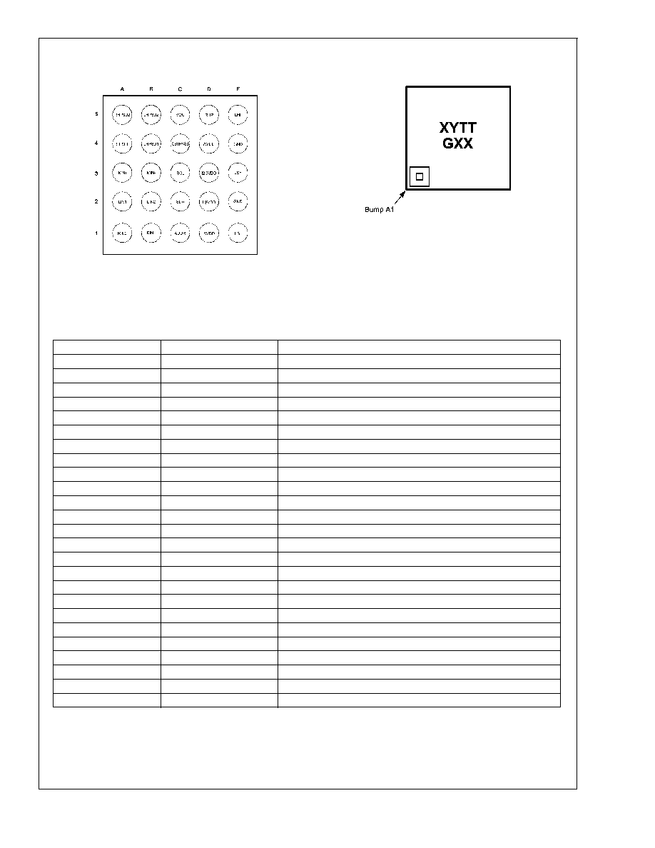
Connection Diagrams
25-Bump micro SMD
micro SMD Marking
201735D2
Top View
20173507
Top View
XY - Date Code
TT - Die Traceability
G - Boomer Family
XX - H1
Pin Descriptions
Bump
Name
Description
A1
R
IN2
Right Input Channel 2 or Right Differential Input -
A2
L
IN1
Left Input Channel 1 or Left Differential Input +
A3
MIN+
Mono Channel Non-inverting Input
A4
RHP
3D1
Right Headphone 3D Input 1
A5
RHP
3D2
Right Headphone 3D Input 2
B1
R
IN1
Right Input Channel 1 or Right Differential Input +
B2
L
IN2
Left Input Channel 2 or Left Differential Input -
B3
MIN-
Mono Channel Inverting Input
B4
L
HP3D1
Left Headphone 3D Input 2
B5
L
HP3D2
Left Headphone 3D Input 1
C1
ADDR
Address Identification
C2
SDA
Serial Data Input
C3
SCL
Serial Clock Input
C4
C
BYPASS
Half-Supply Bypass Capacitor
C5
VOC
Headphone return bias output
D1
AV
DD
Analog Power Supply
D2
LSV
DD
Loudspeaker Power Supply
D3
I2CV
DD
I2C Interface Power Supply
D4
AV
DD
Analog Power Supply
D5
R
HP
Right Headphone Output
E1
LS-
Loudspeaker Output Negative
E2
GND
Ground
E3
LS+
Loudspeaker Output Positive
E4
GND
Ground
E5
L
HP
Left Headphone Output
LM4947
www.national.com
3

Absolute Maximum Ratings
(Note 2)
If Military/Aerospace specified devices are required,
please contact the National Semiconductor Sales Office/
Distributors for availability and specifications.
Supply Voltage
6.0V
Storage Temperature
-65∞C to +150∞C
Input Voltage
-0.3 to V
DD
+0.3
ESD Susceptibility (Note 3)
2.0kV
ESD Machine model (Note 6)
200V
Junction Temperature (T
J
)
150∞C
Solder Information
Vapor Phase (60 sec.)
215∞C
Infrared (15 sec.)
220∞C
Thermal Resistance
JA
(typ) - TLA25CBA
65∞C/W
Operating Ratings
Temperature Range
-40∞C to 85∞C
Supply Voltage (V
DD
)
2.7V
V
DD
5.5V
Supply Voltage (I
2
C)
2.2V
V
DD
5.5V
Supply Voltage (Loudspeaker V
DD
)
2.7V
V
DD
5.5V
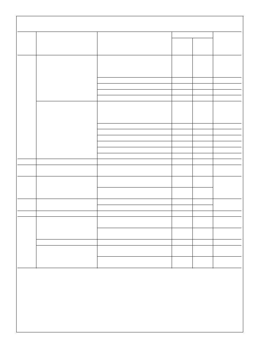
Electrical Characteristics 3.3V
(Notes 2, 7)
The following specifications apply for V
DD
= 3.3V, T
A
= 25∞C, and all gains are set for 0dB unless otherwise specified.
Symbol
Parameter
Conditions
LM4947
Units
(Limits)
Typical
(Note 4)
Limits
(Note 5)
I
DDQ
Quiescent Supply Current
Output Modes 2, 4, 6
V
IN
= 0V; No load,
OCL = 0 (Table 2)
4.5
6.5
mA (max)
Output Modes 1, 3, 5, 7
V
IN
= 0V; No load, BTL,
OCL = 0 (Table 2)
6.5
8
mA (max)
I
SD
Shutdown Current
Output Mode 0
0.1
1
µA (max)
V
OS
Output Offset Voltage
V
IN
= 0V, Mode 7, Mono
2
15
mV (max)
V
IN
= 0V, Mode 7, Headphones
2
15
P
O
Output Power
MONO
OUT
; R
L
= 8
THD+N = 1%; f = 1kHz, BTL, Mode 1
500
400
mW (min)
R
OUT
and L
OUT
; R
L
= 32
THD+N = 1%; f = 1kHz, SE, Mode 4
37
33
mW (min)
THD+N
Total Harmonic Distortion Plus
Noise
MONO
OUT
f = 1kHz, P
OUT
= 250mW;
R
L
= 8
, BTL, Mode 1
0.03
%
R
OUT
and L
OUT
f = 1kHz, P
OUT
= 12mW;
R
L
= 32
, SE, Mode 4
0.02
%
N
OUT
Output Noise
A-weighted, 0dB
inputs terminated, output referred
Speaker; Mode 1
39
µV
Speaker; Mode 3
39
µV
Speaker; Mode 5
42
µV
Speaker; Mode 7
38
µV
Headphone; SE, Mode 2
15
µV
Headphone; SE, Mode 4
15
µV
Headphone; SE, Mode 6
17
µV
Headphone; OCL, Mode 2
12
µV
Headphone; OCL, Mode 4
15
µV
Headphone; OCL, Mode 6
17
µV
LM4947
www.national.com
4
Electrical Characteristics 3.3V
(Notes 2, 7) (Continued)
The following specifications apply for V
DD
= 3.3V, T
A
= 25∞C, and all gains are set for 0dB unless otherwise specified.
Symbol
Parameter
Conditions
LM4947
Units
(Limits)
Typical
(Note 4)
Limits
(Note 5)
PSRR
Power Supply Rejection Ratio
Loudspeaker out
V
RIPPLE
= 200mV
PP
; f = 217Hz,
R
L
= 8
, C
B
= 2.2µF, BTL
All audio inputs terminated to GND;
output referred
BTL, Output Mode 1
79
dB
BTL, Output Mode 3
78
dB
BTL, Output Mode 5
79
dB
BTL, Output Mode 7
80
dB
Power Supply Rejection Ratio
R
OUT
and L
OUT
V
RIPPLE
= 200mV
PP
; f = 217Hz,
R
L
= 32
, C
B
= 2.2µF, BTL
All audio inputs terminated to GND;
output referred
SE, Output Mode 2
78
dB
SE, Output Mode 4
71
dB
SE, Output Mode 6
71
dB
OCL, Output Mode 2
83
dB
OCL, Output Mode 4
74
dB
OCL, Output Mode 6
74
dB
Class D Efficiency
Output Mode 1, 3, 5
86
%
CMRR
Common-Mode-Rejection Ratio
f = 217Hz, V
CM
= 1Vpp,
Mode 1, BTL, R
L
= 8
≠49
dB
XTALK
Crosstalk
Headphone, P
O
= 12mW,
f = 1kHz, OCL, Mode 4, R
L
= 32
≠58
dB
Headphone, P
O
= 12mW,
f = 1kHz, SE, Mode 4, R
L
= 32
≠73
T
WU
Wake-Up Time from Shutdown
C
B
= 2.2µF, OCL, R
L
= 32
90
ms
C
B
= 2.2µF, SE, R
L
= 32
115
Volume Control Step Size Error
±
0.2
dB
Digital Volume Range
Input referred maximum attenuation
-59.5
≠60.25
≠58.75
dB (min)
dB (max)
Input referred maximum gain
+18
17.25
18.75
dB (min)
dB (max)
Mute Attenuation
Output Mode 1, 3, 5
87
dB
MONO_IN Input Impedance
R
IN
and L
IN
Input Impedance
Maximum gain setting
12
8
14
k
(min)
k
(max)
Maximum attenuation setting
100
75
125
k
(min)
k
(max)
LM4947
www.national.com
5