 | ÐлекÑÑоннÑй компоненÑ: LM4982 | СкаÑаÑÑ:  PDF PDF  ZIP ZIP |
Äîêóìåíòàöèÿ è îïèñàíèÿ www.docs.chipfind.ru
LM4982
Ground-Referenced, Ultra Low Noise, 80mW Stereo
Headphone Amplifier with IntelliSense and I2C Volume
Control
General Description
The LM4982 is a ground referenced, variable gain audio
power amplifier capable of delivering 80mW of continuous
average power into a 16
single-ended load with less than
1% THD+N from a 3V power supply. The I
2
C volume control
allows +18 to -76 dB gain settings.
The LM4982 utilizes advanced charge pump technology to
generate the LM4982's negative supply voltage. This elimi-
nates the need for output-coupling capacitors typically used
with single-ended loads.
IntelliSense is a new circuit technology that allows the
LM4982 to detect whether a mono or stereo headphone plug
has been inserted into the output jack.
Boomer audio power amplifiers were designed specifically to
provide high quality output power with a minimal amount of
external components. The LM4982 does not require output
coupling capacitors or bootstrap capacitors, and therefore is
ideally suited for mobile phone and other low voltage appli-
cations where minimal power consumption is a primary re-
quirement.
The LM4982 incorporates selectable low-power consump-
tion shutdown and channel select modes.
The LM4982 contains advanced pop & click circuitry that
eliminates noises which would otherwise occur during
turn-on and turn-off transitions.
Key Specifications
j
Improved PSRR at 217Hz
66dB
j
Stereo Output Power at V
DD
= 3V,
R
L
= 32
, THD+N = 1%
51mW (typ)
j
Shutdown current
0.1µA (typ)
Features
n
Ground referenced outputs
n
I
2
C Volume and mode controls
n
Available in space-saving micro SMD package
n
Ultra low current shutdown mode
n
Advanced pop & click circuitry eliminates noises during
turn-on and turn-off transitions
n
1.6 4.0V operation
n
No output coupling capacitors, snubber networks,
bootstrap capacitors or gain-setting resistors required
n
Mono/Stereo headphone detect
Applications
n
Notebook PCs
n
Desktop PCs
n
Mobile Phones
n
PDAs
n
Portable electronic devices
n
MP3 Players
Boomer
®
is a registered trademark of National Semiconductor Corporation.
February 2006
LM4982
Ground-Referenced,
Ultra
Low
Noise,
80mW
Stereo
Headphone
Amplifier
with
IntelliSense
and
I2C
V
olume
Control
© 2006 National Semiconductor Corporation
DS201614
www.national.com
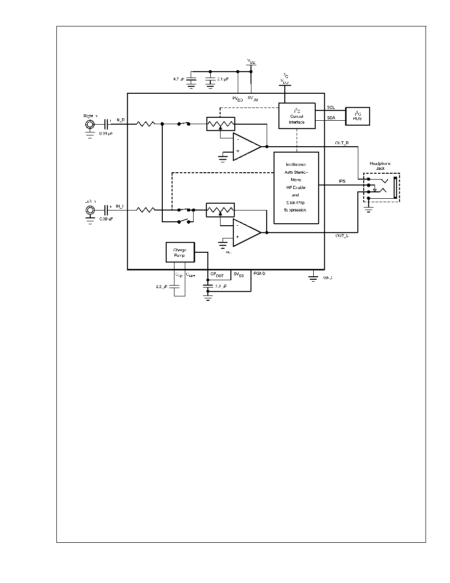
Typical Application
20161466
FIGURE 1. Typical Audio Amplifier Application Circuit
LM4982
www.national.com
2
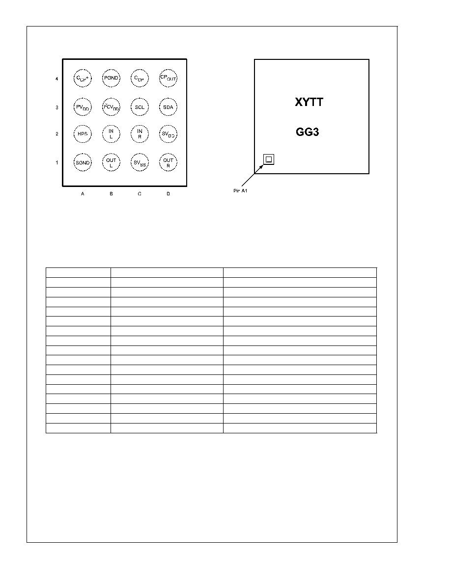
Connection Diagrams
micro SMD Package
micro SMD Marking
20161459
Top View
Order Number LM4982TL
20161401
Top View
XY - Date Code
TT - Lot Traceability
GG3 LM4982
See NS Package Number LM4982TL
Pin Descriptions
Pin Designator
Pin Name
Pin Function
A1
SGND
Amplifier ground
A2
HPE
Headphone sende input
A3
PV
DD
Charge pump / digital power supply
A4
C
CP+
Charge pump fly capacitor positive side
B1
OUT_L
Left channel output
B2
IN_L
Left channel input
B3
I
2
C_V
DD
I
2
C power supply
B4
PGND
Charge pump / digital ground
C1
SV
SS
Amplifier negative supply
C2
IN_R
Right channel input
C3
SCL
I
2
C SCL line
C4
C
CP-
Charge pump fly capacitor negative side
D1
OUT_R
Right channel output
D2
SV
DD
Amplifier positive supply
D3
SDA
I
2
C SDA line
D4
CP
OUT
Charge pump power output
LM4982
www.national.com
3
Absolute Maximum Ratings
(Note 2)
If Military/Aerospace specified devices are required,
please contact the National Semiconductor Sales Office/
Distributors for availability and specifications.
Supply Voltage
4.5V
Storage Temperature
-65°C to +150°C
Input Voltage
-0.3V to V
DD
+0.3V
Power Dissipation (Note 3)
Internally Limited
ESD Susceptibility (Note 4)
2000V
ESD Susceptibility (Note 5)
200V
Junction Temperature
150°C
Thermal Resistance
JA
(typ) - (TLA16XXX)
105°C/W (Note X)
Operating Ratings
Temperature Range
T
MIN
T
A
T
MAX
-40°C
T
A
+85°C
Supply Voltage
1.6V
V
DD
4.0V
Audio Amplifier Electrical Characteristics V
DD
= 3V
(Notes 1, 2)
The following specifications apply for V
DD
= 3V, R
L
= 16
, A
V
= 0dB, unless otherwise specified. Limits apply for T
A
= 25°C.
Symbol
Parameter
Conditions
LM4982
Units
(Limits)
Typical
(Note 6)
Limits (Notes 7,
8)
I
DD
Quiescent Power Supply
Current Full Power Mode
V
IN
= 0V, inputs terminated,
both channels enabled
8.1
11.5
mA (max)
V
IN
= 0V, inputs terminated,
one channel enabled
5.1
7.3
mA
V
IN
= 0V, inputs terminated,
No headphone inserted
2.15
mA
I
SD
Shutdown Current
With SD enabled
0.1
1.5
µA (max)
V
OS
Output Offset Voltage
R
L
= 32
0.7
4.5
mV (max)
A
V
Gain Max and Min settings
[B0:B4] = 00000
70
dB
[B0:B4] = 11111
+18
dB
R
IN
Input Resistance
gain setting 18dB
22
15
29
k
(min)
k
(max)
gain setting 76dB
200
k
P
OUT
Stereo Output Power
THD+N = 1% (max); f = 1kHz,
R
L
= 16
, per channel
47
40
mW (min)
THD+N = 1% (max); f = 1kHz,
R
L
= 32
, per channel
51
mW
THD+N
Total Harmonic Distortion +
Noise
P
O
= 50mW, f = 1kHz
R
L
= 16
, single channel
0.05
%
P
O
= 50mW, f = 1kHz
R
L
= 32
, single channel
0.025
PSRR
Power Supply Rejection Ratio
Full Power Mode
V
RIPPLE
= 200mV
P-P
, input referred
f = 217Hz
66
56
dB
f = 1kHz
55
f = 20kHz
40
SNR
Signal-to-Noise-Ratio
R
L
= 32
, P
OUT
= 20mW,
f = 1kHz, BW = 20Hz to 22kHz
100
dB
T
WU
Wake Up Time From
Shutdown
Charge Pump Wake-Up Time
300
µs
T
WU
Wake Up Time
Headphone Sense Debounce Time
200
ms
X
TALK
Crosstalk
R
L
= 16
, P
OUT
= 1.6mW,
f = 1kHz, A-weighted filter
70
dB
Z
OUT
Output Impedance
In Shutdown Mode
180
k
I
L
Input Leakage
±
0.1
nA
Vih
HPS in threshold
0.9 x V
DD
[min]
V
Vil
HPS in threshold
0.7 x V
DD
[max]
V
LM4982
www.national.com
4
Audio Amplifier Electrical Characteristics V
DD
= 3V
(Notes 1, 2) (Continued)
The following specifications apply for V
DD
= 3V, R
L
= 16
, A
V
= 0dB, unless otherwise specified. Limits apply for T
A
= 25°C.
Symbol
Parameter
Conditions
LM4982
Units
(Limits)
Typical
(Note 6)
Limits (Notes 7,
8)
R
INT
Intellisense Threshold
Resistance
6
3
9
(min)
(max)
Control Interface Electrical Characteristics
(Notes 1, 2)
The following specifications apply for 1.6V
<
V
DD
<
4.0V, unless otherwise specified. Limits apply for T
A
= 25°C.
Symbol
Parameter
Conditions
LM4982
Units
(Limits)
Typical
(Note 6)
Limits (Notes 7,
8)
t
1
SCL period
2.5
µs (min)
t
2
SDA Setup Time
100
ns (min)
t
3
SDA Stable Time
0
ns (min)
t
4
Start Condition Time
100
ns (min)
t
5
Stop Condition Time
100
ns (min)
V
IH
0.7 x I
2
CV
DD
V (min)
V
IL
0.3 x I
2
CV
DD
V (max)
Note 1: All voltages are measured with respect to the GND pin unless otherwise specified.
Note 2: Absolute Maximum Ratings indicate limits beyond which damage to the device may occur. Operating Ratings indicate conditions for which the device is
functional but do not guarantee specific performance limits. Electrical Characteristics state DC and AC electrical specifications under particular test conditions which
guarantee specific performance limits. This assumes that the device is within the Operating Ratings. Specifications are not guaranteed for parameters where no limit
is given, however, the typical value is a good indication of device performance.
Note 3: The maximum power dissipation must be derated at elevated temperatures and is dictated by T
JMAX
,
JA
, and the ambient temperature, T
A
. The maximum
allowable power dissipation is P
DMAX
= (T
JMAX
- T
A
) /
JA
or the number given in Absolute Maximum Ratings, whichever is lower. For the LM4982, see power
derating currents for more information.
Note 4: Human body model, 100pF discharged through a 1.5k
resistor.
Note 5: Machine Model, 220pF - 240pF discharged through all pins.
Note 6: Typicals are measured at +25°C and represent the parametric norm.
Note 7: Limits are guaranteed to National's AOQL (Average Outgoing Quality Level).
Note 8: Datasheet min/max specification limits are guaranteed by design, test, or statistical analysis.
LM4982
www.national.com
5
Document Outline