LM4985
Stereo 135mW Low Noise Headphone Amplifier with
Selectable Capacitively Coupled or Output
Capacitor-less (OCL) Output and Digitally Controlled
(I
2
C) Volume Control
General Description
The LM4985 is a stereo audio power amplifier with internal
digitally controlled volume control. This amplifier is capable
of delivering 68mW
RMS
per channel into a 16
load or
38mW
RMS
per channel into a 32
load at 1% THD when
powered by a 3.6V power supply and operating in the OCL
mode.
Boomer audio power amplifiers were designed specifically to
provide high quality output power with a minimal amount of
external components. To that end, the LM4985 features two
functions that optimize system cost and minimize PCB area:
an integrated, digitally controlled (I
2
C bus) volume control
and an operational mode that eliminates output signal cou-
pling capacitors (OCL mode). Since the LM4985 does not
require bootstrap capacitors, snubber networks, or output
coupling capacitors, it is optimally suited for low-power, bat-
tery powered portable systems. For added design flexibility,
the LM4985 can also be configured for single-ended capaci-
tively coupled outputs.
The LM4985 features a current shutdown mode for mi-
cropower dissipation and thermal shutdown protection.
Key Specifications (V
DD
= 3.6V)
j
PSRR: 217Hz and 1kHz
Output Capacitor-less (OCL)
f
RIPPLE
= 217Hz
77dB (typ)
f
RIPPLE
= 1kHz
76dB (typ)
Capacitor Coupled (C-CUPL)
f
RIPPLE
= 217Hz
63dB (typ)
f
RIPPLE
= 1kHz
62dB (typ)
j
Output Power per channel
(f
IN
= 1kHz, THD+N = 1%),
R
L
= 16
,OCL
V
DD
= 2.5V
31mW (typ)
V
DD
= 3.6V
68mW (typ)
V
DD
= 5.0V
135mW (typ)
j
THD+N (f = 1kHz)
R
LOAD
= 16
, OCL, P
OUT
= 60mW
0.60
R
LOAD
= 32
, OCL, P
OUT
= 33mW
0.031
j
Shutdown Current
0.1�A (typ)
Features
n
OCL or capacitively coupled outputs (patent pending)
n
I
2
C Digitally Controlled Volume Control
n
Available in space-saving 0.4mm lead-pitch micro SMD
package
n
Volume control range: �76dB to +18dB
n
Ultra low current shutdown mode
n
2.3V - 5.5V operation
n
Ultra low noise
Applications
n
Mobile Phones
n
PDAs
n
Portable electronics devices
n
MP3 Players
Boomer
�
is a registered trademark of National Semiconductor Corporation.
May 2006
LM4985
Stereo
135mW
Low
Noise
Headphone
Amplifier
with
Selectable
Capacitive
Coupled
or
Capacitor-less
(OCL)
Output
and
Digitally
Controlled
(I
2
C)
V
olume
Control
� 2006 National Semiconductor Corporation
DS201697
www.national.com
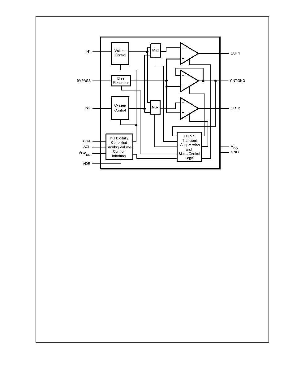
Block Diagram
201697E9
FIGURE 1. Block Diagram
LM4985
www.national.com
2
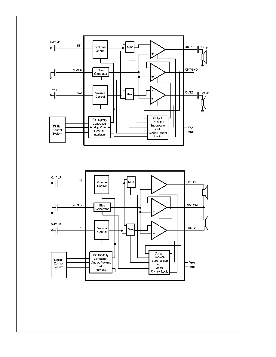
Typical Application
201697F0
FIGURE 2. Typical Capacitively Coupled Output Configuration Circuit
201697F1
FIGURE 3. Typical OCL Output Configuration Circuit
LM4985
www.national.com
3
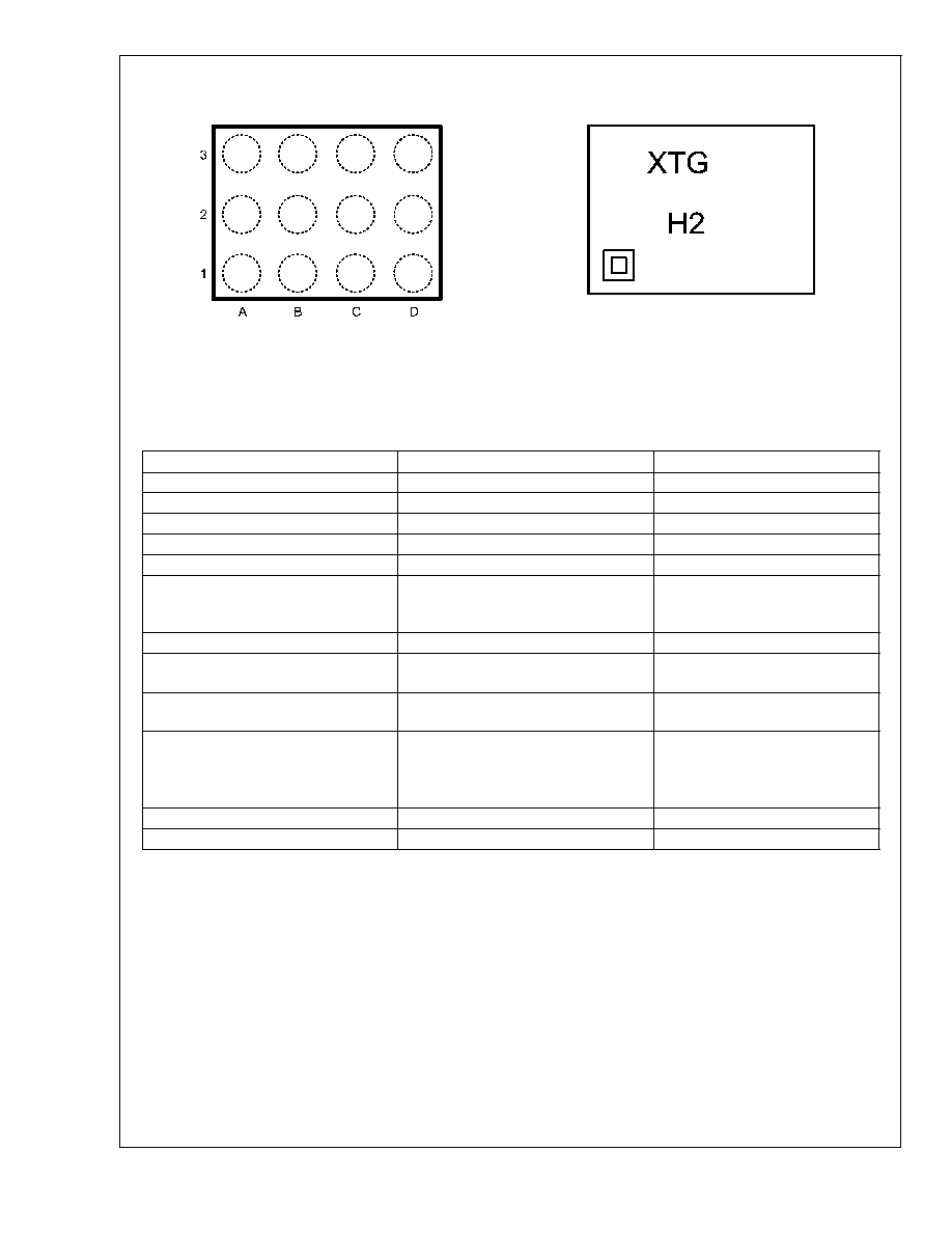
Connection Diagrams
micro SMD Package
micro SMD Marking
20169715
Top View
Order Number LM4985TM
See NS Package Number TMD12AAA
20169730
Top View
X � Date Code
T � Die Traceability
G � Boomer Family
H2 � LM4985TM
Pin Reference, Name, and Function
Reference
Name
Function
A1
ADR
I
2
C serial interface address input.
A2
IN2
Analog signal input two.
A3
OUT2
Power amplifier two output.
B1
SDA
I
2
C serial interface data input.
B2
BYPASS
The internal V
DD
/2 ac bypass node.
B3
CNTGND
In OCL mode, this is the ac ground
return. It is biased to V
DD
/2. Leave
unconnected for C-CUPL mode.
C1
SCL
I2C serial interface clock input.
C2
GND
The LM4985's power supply ground
input.
C3
V
DD
The LM4985's power supply voltage
input.
D1
I
2
CV
DD
I
2
C serial interface power supply
input. Can be connected to the same
supply that is connected to the V
DD
pin.
D2
IN1
Analog signal input one.
D3
OUT1
Power amplifier one output.
LM4985
www.national.com
4

Absolute Maximum Ratings
(Notes 1, 2)
If Military/Aerospace specified devices are required,
please contact the National Semiconductor Sales Office/
Distributors for availability and specifications.
Supply Voltage (V
DD
, I
2
CV
DD
)
6.0V
Storage Temperature
-65�C to +150�C
Input Voltage (IN1, IN2, OUT1,
OUT2, BYPASS, CNTGND, GND
pins relative to the V
DD
pin)
-0.3V to V
DD
+ 0.3V
Input Voltage (ADR, SDA, SCL
pins, relative to the I
2
CV
DD
pin)
-0.3V to I
2
CV
DD
+ 0.3V
Power Dissipation (Note 3)
Internally Limited
ESD Susceptibility (Note 4)
2000V
ESD Susceptibility (Note 5)
200V
Junction Temperature
150�C
Thermal Resistance
JA
109�C/W
Operating Ratings
Temperature Range
T
MIN
T
A
T
MAX
-40�C
T
A
85�C
Supply Voltage
V
DD
2.3V
V
CC
5.5V
I
2
CV
DD
1.7V
I
2
CV
DD
5.5V
Electrical Characteristics V
DD
= 5V
(Notes 1, 2)
The following specifications apply for R
L
= 16
, f = 1kHz, and C
B
= 4.7�F unless otherwise specified. Limits apply to T
A
=
25�C.
Symbol
Parameter
Conditions
LM4985
Units
(Limits)
Typ
(Note 6)
Limit
(Notes 7,
8)
I
DD
Quiescent Power Supply Current
V
IN
= 0V, I
OUT
= 0A
Single-Channel no load OCL
Single-Channel no load C-CUPL
Dual-Channel no load OCL
Dual-Channel no load C-CUPL
2
1.5
3
2.3
4.9
3.8
mA (max)
I
SD
Shutdown Current
V
SHUTDOWN
= GND
0.1
1.0
�A (max)
V
SDIH
Logic Voltage Input High
3.5
V (min)
V
SDIL
Logic Voltage Input Low
1.5
V (max)
P
O
Output Power
THD
1%; f
IN
= 1kHz
R
LOAD
= 16
OCL
135
115
R
LOAD
= 16
C-CUPL
135
mW (min)
R
LOAD
= 32
OCL
79
70
R
LOAD
= 32
C-CUPL
80
THD+N
Total Harmonic Distortion + Noise
R
LOAD
= 16
OCL, P
O
= 100mW
R
LOAD
= 16
C-CUPL, P
O
= 100mW
R
LOAD
= 32
OCL, P
O
= 60mW
R
LOAD
= 32
C-CUPL, P
O
= 70mW
0.08
0.02
0.04
0.01
%
V
ON
Output Noise Voltage
V
IN
= AC GND, A
V
= 0dB, A-weighted
15
�V
PSRR
Power Supply Rejection Ratio
V
RIPPLE
= 200mVp-p (Note 9)
f
IN
= 217Hz sinewave
OCL
C-CUPL
77
65
57
dB (min)
f
IN
= 1kHz sinewave
OCL
C-CUPL
77
65
60
Xtalk
Channel-to-channel Crosstalk
P
out
= 40mW. OCL
R
LOAD
= 16
R
LOAD
= 32
51
56
dB
P
out
= 50mW. C-CUPL
R
LOAD
= 16
R
LOAD
= 32
58
68
dB
LM4985
www.national.com
5