 | –≠–Ľ–Ķ–ļ—ā—Ä–ĺ–Ĺ–Ĺ—č–Ļ –ļ–ĺ–ľ–Ņ–ĺ–Ĺ–Ķ–Ĺ—ā: LM5021 | –°–ļ–į—á–į—ā—Ć:  PDF PDF  ZIP ZIP |
LM5021
AC-DC Current Mode PWM Controller
General Description
The LM5021 off-line pulse width modulation (PWM) control-
ler contains all of the features needed to implement highly
efficient off-line single-ended flyback and forward power con-
verters using current-mode control. The LM5021 features
include an ultra-low (25 ĶA) start-up current, which mini-
mizes power losses in the high voltage start-up network. A
skip cycle mode reduces power consumption with light loads
for energy conserving applications (ENERGY STAR
ģ
,
CECP, etc.). Additional features include under-voltage lock-
out, cycle-by-cycle current limit, hiccup mode overload pro-
tection, slope compensation, soft-start and oscillator syn-
chronization capability. This high performance 8-pin IC has
total propagation delays less than 100nS and a 1MHz ca-
pable oscillator that is programmed with a single resistor.
Features
n
Ultra Low Start-up Current (25 ĶA maximum)
n
Current Mode Control
n
Skip Cycle Mode for Low Standby Power
n
Single Resistor Programmable Oscillator
n
Synchronizable Oscillator
n
Adjustable Soft-start
n
Integrated 0.7A Peak Gate Driver
n
Direct Opto-Coupler Interface
n
Maximum Duty Cycle Limiting (80% for LM5021-1 or
50% for LM5021-2)
n
Slope Compensation for (LM5021-1 Only)
n
Under Voltage Lockout (UVLO) with Hysteresis
n
Cycle-by-Cycle Over-Current Protection
n
Hiccup Mode for Continuous Overload Protection
n
Leading Edge Blanking of Current Sense Signal
n
Packages: MSOP-8 or MDIP-8
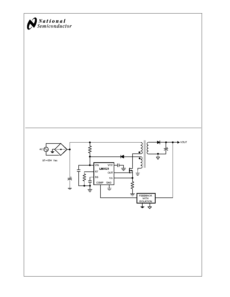
Simplified Application Diagram
20144201
May 2005
LM5021
AC-DC
Current
Mode
PWM
Controller
© 2005 National Semiconductor Corporation
DS201442
www.national.com

Connection Diagram
Top View
20144202
MSOP-8 and MDIP-8
Ordering Information
Order Number
Description
Package Type
Supplied As
LM5021MM-1
80% Duty Cycle Limit
MSOP-8
Available Soon
LM5021MMX-1
80% Duty Cycle Limit
MSOP-8
Available Soon
LM5021NA-1
80% Duty Cycle Limit
MDIP-8
40 Units per Rail
LM5021MM-2
50% Duty Cycle Limit
MSOP-8
Available Soon
LM5021MMX-2
50% Duty Cycle Limit
MSOP-8
Available Soon
LM5021NA-2
50% Duty Cycle Limit
MDIP-8
40 Units per Rail
Pin Description
PIN
NAME
DESCRIPTION
APPLICATION INFORMATION
1
COMP
Control input for the Pulse Width Modulator
and Hiccup comparators.
COMP pull-up is provided by an internal 5K resistor
which may be used to bias an opto-coupler transistor.
2
VIN
Input voltage.
Input to start-up regulator. The VIN pin is clamped at
36V by an internal zener diode.
3
VCC
Output of a linear bias supply regulator.
Nominally 8.5V.
VCC provides bias to controller and gate drive sections
of the LM5021. An external capacitor must be connected
from this pin to ground.
4
OUT
MOSFET gate driver output.
High current output to the external MOSFET gate input
with source/sink current capability of 0.3A and 0.7A
respectively.
5
GND
Ground return.
6
CS
Current Sense input.
Current sense input for current mode control and
over-current protection. Current limiting is accomplished
using a dedicated current sense comparator. If the CS
comparator input exceeds 0.5 Volts the OUT pin
switches low for cycle-by-cycle current limit. CS is held
low for 90ns after OUT switches high to blank the
leading edge current spike.
7
RT / SYNC
Oscillator timing resistor pin and
synchronization input.
An external resistor connected from RT to GND sets the
oscillator frequency. This pin will also accept
synchronization pulses from an external clock.
8
SS
Soft-start / Hiccup time
An external capacitor and an internal 22 ĶA current
source set the soft-start ramp. The soft -start capacitor
controls both the soft-start rate and the hiccup mode
period.
LM5021
www.national.com
2

Absolute Maximum Ratings
(Note 1)
If Military/Aerospace specified devices are required,
please contact the National Semiconductor Sales Office/
Distributors for availability and specifications.
VIN to GND
-0.3V to 30V
VIN Clamp Continuous Current
5mA
CS to GND
-0.3V to 1.25V
RT to GND
-0.3V to 5.5V
All other pins to GND
-0.3V to 7.0V
ESD Rating (Note 2)
Human Body Model
2kV
Storage Temperature
-65įC to +150įC
Operating Junction Temperature
+150įC
Operating Ratings
(Note 1)
VIN Voltage (Note 5)
8V to 30V
Junction Temperature
-40įC to +125įC
Electrical Characteristics
Specifications in standard type face are for T
J
= +25įC and those in boldface
type apply over the full Operating Junction Temperature Range. Unless otherwise specified: V
IN
= 15V, R
T
= 44.2K
.
(Note 3)
Symbol
Parameter
Conditions
Min
Typ
Max
Unit
STARTUP CIRCUIT
Start Up Current
Before VCC Enable
18
25
ĶA
VCC Regulator enable threshold
17
20
23
V
VCC Regulator disable
threshold
7.25
V
VIN ESD Clamp voltage
I = 5mA
30
36
40
V
I
VIN
Operating supply current
COMP = 0VDC
2.5
3.75
mA
VCC SUPPLY
Controller enable threshold
6.5
7
7.5
V
Controller disable threshold
5.3
5.8
6.3
V
VCC regulated output
No External Load
8
8.5
9
V
VCC dropout voltage (VIN -
VCC)
I = 5 mA
1.7
V
VCC regulator current limit
VCC = 7.5V (Note
4)
15
22
mA
SKIP CYCLE MODE COMPARATOR
Skip Cycle mode enable
threshold
1
/
3
[COMP - 1.25V]
75
125
175
mV
Skip Cycle mode hysteresis
5
mV
CURRENT LIMIT
CS limit to OUT delay
CS stepped from 0
to 0.6V, time to OUT
transition low, C
load
= 0.
35
ns
CS limit threshold
0.45
0.5
0.55
V
Leading Edge Blanking time
90
ns
CS blanking sinking impedance
35
55
SOFT-START
V
SS-OCV
SS pin open-circuit voltage
4.3
5.2
6.1
V
Soft-start Current Source
15
22
30
ĶA
Soft-start to COMP Offset
0.35
0.55
0.75
V
COMP sinking impedance
During SS ramp
60
OSCILLATOR
Frequency1 (RT = 44.2K)
135
150
165
kHz
Frequency2 (RT = 13.3K)
440
500
560
kHz
Sync threshold
2.4
3.2
3.8
V
LM5021
www.national.com
3

Electrical Characteristics
Specifications in standard type face are for T
J
= +25įC and those in boldface type
apply over the full Operating Junction Temperature Range. Unless otherwise specified: V
IN
= 15V, R
T
= 44.2K
. (Note
3) (Continued)
Symbol
Parameter
Conditions
Min
Typ
Max
Unit
PWM COMPARATOR
COMP to OUT delay
COMP set to 2V
CS stepped 0 to
0.4V, time to OUT
transition low, C
load
= 0.
20
ns
Min Duty Cycle
COMP = 0V
0
%
Max Duty Cycle (-1 Device)
75
80
85
%
Max Duty Cycle (-2 Device)
50
%
COMP to PWM comparator gain
0.33
COMP Open Circuit Voltage
4.2
5.1
6
V
COMP at Max Duty Cycle
2.75
V
COMP Short Circuit Current
COMP = 0V
0.6
1.1
1.5
mA
SLOPE COMPENSATION
Slope Comp Amplitude
(LM5021-1 only)
CS pin to PWM
Comparator offset at
maximum duty cycle
70
90
110
mV
OUTPUT SECTION
OUT High Saturation
IOUT = 50mA, VCC
- OUT
0.6
1.1
V
OUT Low Saturation
IOUT = 100mA
0.3
1
V
Peak Source Current
OUT = VCC/2.
0.3
A
Peak Sink Current
OUT = VCC/2.
0.7
A
Rise time
C
load
= 1nF
25
ns
Fall time
C
load
= 1nF
10
ns
HICCUP MODE
V
OVLD
Over load detection threshold
COMP pin
V
SS-OCV
≠ 0.8 V
SS-OCV
≠ 0.6 V
SS-OCV
≠ 0.4
V
V
HIC
Hiccup mode threshold
SS pin
V
SS-OCV
≠ 0.8 V
SS-OCV
≠ 0.6 V
SS-OCV
≠ 0.4
V
V
RST
Hiccup mode Restart threshold
SS pin
0.1
0.3
0.5
V
I
DTCS
Dead-time current source
0.1
0.25
0.4
ĶA
I
OVCS
Overload detection timer current
source
6
10
14
ĶA
THERMAL RESISTANCE
JA
MSOP-8 Junction to Ambient
0 LFM
200
įC/W
JA
MDIP-8 Junction to Ambient
0 LFM
107
įC/W
Note 1: Absolute Maximum Ratings are limits beyond which damage to the device may occur. Operating Ratings are conditions under which operation of the device
is intended to be functional. For guaranteed specifications and test conditions, see the Electrical Characteristics.
Note 2: The human body model is a 100 pF capacitor discharged through a 1.5k
resistor into each pin.
Note 3: Min and Max limits are 100% production tested at 25įC. Limits over the operating temperature range are guaranteed through correlation using Statistical
Quality Control (SQC) methods. Limits are used to calculate National's Average Outgoing Quality Level (AOQL).
Note 4: Device thermal limitations may limit usable range.
Note 5: After initial turn-on at VIN = 20V.
LM5021
www.national.com
4
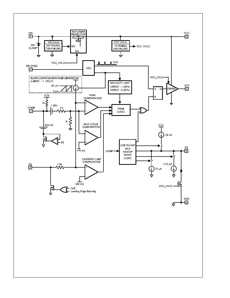
Simplified Block Diagram
20144203
FIGURE 1.
LM5021
www.national.com
5