 | –≠–ª–µ–∫—Ç—Ä–æ–Ω–Ω—ã–π –∫–æ–º–ø–æ–Ω–µ–Ω—Ç: LM6211 | –°–∫–∞—á–∞—Ç—å:  PDF PDF  ZIP ZIP |
LM6211
Low Noise, RRO Operational Amplifier with CMOS Input
and 24V Operation
General Description
The LM6211 is a wide bandwidth, low noise op amp with a
wide supply voltage range and a low input bias current. The
LM6211 operates with a single supply voltage of 5V to 24V,
is unity gain stable, has a ground-sensing CMOS input
stage, and offers rail-to-rail output swing.
The LM6211 is designed to provide optimal performance in
high voltage, low noise systems. The LM6211 has a unity
gain bandwidth of 20 MHz and an input referred voltage
noise density of 5.5 nV/
at 10 kHz. The LM6211
achieves these specifications with a low supply current of
only 1 mA. The LM6211 has a low input bias current of
2.3 pA, an output short circuit current of 25 mA and a slew
rate of 5.6 V/us. The LM6211 also features a low common-
mode input capacitance of 5.5 pF which makes it ideal for
use in wide bandwidth and high gain circuits. The LM6211 is
well suited for low noise applications that require an op amp
with very low input bias currents and a large output voltage
swing, like active loop-filters for wide-band PLLs. A low total
harmonic distortion, 0.01% at 1 kHz with loads as high as
600
, also makes the LM6211 ideal for high fidelity audio
and microphone amplifiers.
The LM6211 is available in the small SOT package, allowing
the user to implement ultra-small and cost effective board
layouts.
Features
(Typical 24V supply unless otherwise noted)
n
Supply voltage range
5V to 24V
n
Input referred voltage noise
5.5 nV/
n
Unity gain bandwidth
20 MHz
n
1/f corner frequency
400 Hz
n
Slew rate
5.6 V/µs
n
Supply current
1.05 mA
n
Low input capacitance
5.5 pF
n
Temperature range
-40∞C to 125∞C
n
Total harmonic distortion
0.01%
@
1 kHz, 600
n
Output short circuit current
25 mA
Applications
n
PLL loop filters
n
Low noise active filters
n
Strain gauge amplifiers
n
Low noise microphone amplifiers
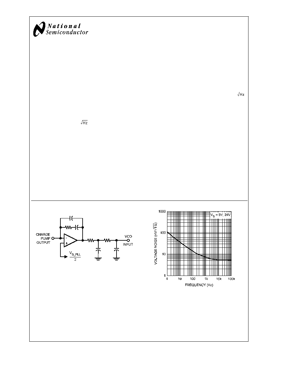
Typical Application
20120303
20120304
May 2006
LM621
1
Low
Noise,
RRO
Op-Amp
with
CMOS
Input
and
24V
Operation
© 2006 National Semiconductor Corporation
DS201203
www.national.com

Absolute Maximum Ratings
(Note 1)
If Military/Aerospace specified devices are required,
please contact the National Semiconductor Sales Office/
Distributors for availability and specifications.
ESD Tolerance (Note 2)
Human Body Model
2000V
Machine Model
200V
V
IN
Differential
±
0.3V
Supply Voltage (V
S
= V
+
≠ V
-
)
25V
Voltage at Input/Output pins
V
+
+0.3V, V
-
-0.3V
Storage Temperature Range
-65∞C to +150∞C
Junction Temperature (Note 3)
+150∞C
Soldering Information
Infrared or Convection (20 sec)
235∞C
Wave Soldering Lead Temp. (10 sec)
260∞C
Operating Ratings
(Note 1)
Temperature Range
-40∞C to +125∞C
Supply Voltage (V
S
= V
+
≠ V
-
)
5V to 24V
Package Thermal Resistance (
JA
(Note 3))
5-Pin SOT23
178∞C/W
5V Electrical Characteristics
(Note 4)
Unless otherwise specified, all limits are guaranteed for T
A
= 25∞C, V
+
= 5V, V
-
= 0V, V
CM
= V
O
= V
+
/2. Boldface limits apply
at the temperature extremes.
Symbol
Parameter
Conditions
Min
(Note 6)
Typ
(Note 5)
Max
(Note 6)
Units
V
OS
Input Offset Voltage
V
CM
= 0.5V
0.1
±
2.5
±
2.8
mV
TC V
OS
Input Offset Average Drift
V
CM
= 0.5V (Note 7)
2
µV/C
I
B
Input Bias Current
V
CM
= 0.5V (Notes 8, 9)
0.5
5
10
pA
nA
I
OS
Input Offset Current
V
CM
= 0.5V
0.1
pA
CMRR
Common Mode Rejection
Ratio
0 V
V
CM
3V
0.4 V
V
CM
2.3 V
83
70
98
dB
PSRR
Power Supply Rejection Ratio
V
+
= 5V to 24V, V
CM
= 0.5V
85
78
98
dB
V
+
= 4.5V to 25V, V
CM
= 0.5V
80
95
CMVR
Input Common-Mode Voltage
Range
CMRR
65 dB
CMRR
60 dB
0
0
3.3
2.4
V
A
VOL
Large Signal Voltage Gain
V
O
= 0.35V to 4.65, R
L
= 2 k
to V
+
/2
82
80
110
dB
V
O
= 0.25V to 4.75, R
L
= 10 k
to V
+
/2
85
82
110
V
O
Output Swing High
R
L
= 2 k
to V
+
/2
50
150
165
mV from
rail
R
L
= 10 k
to V
+
/2
20
85
90
Output Swing Low
R
L
= 2 k
to V
+
/2
39
150
170
R
L
= 10 k
to V
+
/2
13
85
90
I
OUT
Output Short Circuit Current
Sourcing to V
+
/2
V
ID
= 100 mV (Note 10)
13
10
16
mA
Sinking to V
+
/2
V
ID
= -100 mV (Note 10)
20
10
30
I
S
Supply Current
0.96
1.10
1.25
mA
SR
Slew Rate
A
V
= +1, 10% to 90% (Note 11)
5.5
V/µs
GBW
Gain Bandwidth Product
17
MHz
e
n
Input-Referred Voltage Noise
f = 10 kHz
5.5
nV/
f = 1 kHz
6.0
i
n
Input-Referred Current Noise
f = 1 kHz
0.01
pA/
LM621
1
www.national.com
2

5V Electrical Characteristics
(Note 4)
(Continued)
Unless otherwise specified, all limits are guaranteed for T
A
= 25∞C, V
+
= 5V, V
-
= 0V, V
CM
= V
O
= V
+
/2. Boldface limits apply
at the temperature extremes.
Symbol
Parameter
Conditions
Min
(Note 6)
Typ
(Note 5)
Max
(Note 6)
Units
THD
Total Harmonic Distortion
A
V
= 2, R
L
= 600
to V
+
/2
0.01
%
24V Electrical Characteristics
(Note 4)
Unless otherwise specified, all limits are guaranteed for T
A
= 25∞C, V
+
= 24V, V
-
= 0V, V
CM
= V
O
= V
+
/2. Boldface limits apply
at the temperature extremes.
Symbol
Parameter
Conditions
Min
(Note 6)
Typ
(Note 5)
Max
(Note 6)
Units
V
OS
Input Offset Voltage
V
CM
= 0.5V
0.25
±
2.7
±
3.0
mV
TC V
OS
Input Offset Average Drift
V
CM
= 0.5V (Note 7)
±
2
µV/C
I
B
Input Bias Current
V
CM
= 0.5V (Notes 8, 9)
2
25
10
pA
nA
I
OS
Input Offset Current
V
CM
= 0.5V
0.1
pA
CMRR
Common Mode Rejection
Ratio
0
V
CM
21V
0.4
V
CM
20V
85
70
105
dB
PSRR
Power Supply Rejection Ratio
V
+
= 5V to 24V, V
CM
= 0.5V
85
78
98
dB
V
+
= 4.5V to 25V, V
CM
= 0.5V
80
98
CMVR
Input Common-Mode Voltage
Range
CMRR
65 dB
CMRR
60 dB
0
0
21.5
20.5
V
A
VOL
Large Signal Voltage Gain
V
O
= 1.5V to 22.5V, R
L
= 2 k
to V
+
/2
82
77
120
dB
V
O
= 1V to 23V, R
L
= 10 k
to V
+
/2
85
82
120
V
O
Output Swing High
R
L
= 2 k
to V
+
/2
212
400
520
mV from
rail
R
L
= 10 k
to V
+
/2
48
150
165
Output Swing Low
R
L
= 2 k
to V
+
/2
150
350
420
R
L
= 10 k
to V
+
/2
38
150
170
I
OUT
Output Short Circuit Current
Sourcing to V
+
/2
V
ID
= 100 mV (Note 10)
20
15
25
mA
Sinking to V
+
/2
V
ID
= -100 mV (Note 10)
30
20
38
I
S
Supply Current
1.05
1.25
1.40
mA
SR
Slew Rate
A
V
= +1, V
O
= 18 V
PP
10% to 90% (Note 11)
5.6
V/µs
GBW
Gain Bandwidth Product
20
MHz
e
n
Input-Referred Voltage Noise
f = 10 kHz
5.5
nV/
f = 1 kHz
6.0
i
n
Input-Referred Current Noise
f = 1 kHz
0.01
pA/
THD
Total Harmonic Distortion
A
V
= 2, R
L
= 2 k
to V
+
/2
0.01
%
LM621
1
www.national.com
3

Note 1: Absolute Maximum Ratings indicate limits beyond which damage to the device may occur. Operating Ratings indicate conditions for which the device is
intended to be functional, but specific performance is not guaranteed. For guaranteed specifications and the test conditions, see the Electrical Characteristics Tables.
Note 2: Human Body Model is 1.5 k
in series with 100 pF. Machine Model is 0 in series with 200 pF.
Note 3: The maximum power dissipation is a function of T
J(MAX)
,
JA
, and T
A
. The maximum allowable power dissipation at any ambient temperature is
P
D
= (T
J(MAX)
- T
A
)/
JA
. All numbers apply for packages soldered directly onto a PC board.
Note 4: Electrical table values apply only for factory testing conditions at the temperature indicated. Factory testing conditions result in very limited self-heating of
the device.
Note 5: Typical values represent the most likely parametric norm at the time of characterization.
Note 6: Limits are 100% production tested at 25∞C. Limits over the operating temperature range are guaranteed through correlations using the Statistical Quality
Control (SQC) method.
Note 7: Offset voltage average drift is determined by dividing the change in V
OS
at the temperature extremes into the total temperature change.
Note 8: Positive current corresponds to current flowing into the device.
Note 9: Input bias current is guaranteed by design.
Note 10: The device is short circuit protected and can source or sink its limit currents continuously. However, care should be taken such that when the output is
driving short circuit currents, the inputs do not see more than
±
0.3V differential voltage.
Note 11: Slew rate is the average of the rising and falling slew rates.
Connection Diagram
5-Pin SOT23
20120301
Top View
Ordering Information
Package
Part Number
Package Marking
Transport Media
NSC Drawing
5-Pin SOT-23
LM6211MF
AT1A
1k Units Tape and Reel
MF05A
LM6211MFX
3k Units Tape and Reel
LM621
1
www.national.com
4

Typical Performance Characteristics
Unless otherwise specified, T
A
= 25∞C, V
S
= 24V, V
+
= V
S
,
V
-
= 0 V, V
CM
= V
S
/2.
Supply Current vs. Supply Voltage
V
OS
vs. Supply Voltage
20120318
20120319
V
OS
vs. V
CM
V
OS
vs. V
CM
20120320
20120321
Input Bias Current vs. V
CM
Input Bias Current vs. V
CM
20120350
20120351
LM621
1
www.national.com
5